EP1729332B1 - Schedule control method in spin etching - Google Patents
Schedule control method in spin etching Download PDFInfo
- Publication number
- EP1729332B1 EP1729332B1 EP04722390.4A EP04722390A EP1729332B1 EP 1729332 B1 EP1729332 B1 EP 1729332B1 EP 04722390 A EP04722390 A EP 04722390A EP 1729332 B1 EP1729332 B1 EP 1729332B1
- Authority
- EP
- European Patent Office
- Prior art keywords
- etching
- wafer
- weight
- solution
- rate
- Prior art date
- Legal status (The legal status is an assumption and is not a legal conclusion. Google has not performed a legal analysis and makes no representation as to the accuracy of the status listed.)
- Expired - Fee Related
Links
Images


Classifications
-
- H—ELECTRICITY
- H01—ELECTRIC ELEMENTS
- H01L—SEMICONDUCTOR DEVICES NOT COVERED BY CLASS H10
- H01L21/00—Processes or apparatus adapted for the manufacture or treatment of semiconductor or solid state devices or of parts thereof
- H01L21/02—Manufacture or treatment of semiconductor devices or of parts thereof
- H01L21/04—Manufacture or treatment of semiconductor devices or of parts thereof the devices having at least one potential-jump barrier or surface barrier, e.g. PN junction, depletion layer or carrier concentration layer
- H01L21/18—Manufacture or treatment of semiconductor devices or of parts thereof the devices having at least one potential-jump barrier or surface barrier, e.g. PN junction, depletion layer or carrier concentration layer the devices having semiconductor bodies comprising elements of Group IV of the Periodic System or AIIIBV compounds with or without impurities, e.g. doping materials
- H01L21/30—Treatment of semiconductor bodies using processes or apparatus not provided for in groups H01L21/20 - H01L21/26
- H01L21/302—Treatment of semiconductor bodies using processes or apparatus not provided for in groups H01L21/20 - H01L21/26 to change their surface-physical characteristics or shape, e.g. etching, polishing, cutting
- H01L21/306—Chemical or electrical treatment, e.g. electrolytic etching
- H01L21/3065—Plasma etching; Reactive-ion etching
-
- H—ELECTRICITY
- H01—ELECTRIC ELEMENTS
- H01L—SEMICONDUCTOR DEVICES NOT COVERED BY CLASS H10
- H01L22/00—Testing or measuring during manufacture or treatment; Reliability measurements, i.e. testing of parts without further processing to modify the parts as such; Structural arrangements therefor
- H01L22/20—Sequence of activities consisting of a plurality of measurements, corrections, marking or sorting steps
-
- H—ELECTRICITY
- H01—ELECTRIC ELEMENTS
- H01L—SEMICONDUCTOR DEVICES NOT COVERED BY CLASS H10
- H01L21/00—Processes or apparatus adapted for the manufacture or treatment of semiconductor or solid state devices or of parts thereof
- H01L21/02—Manufacture or treatment of semiconductor devices or of parts thereof
- H01L21/04—Manufacture or treatment of semiconductor devices or of parts thereof the devices having at least one potential-jump barrier or surface barrier, e.g. PN junction, depletion layer or carrier concentration layer
- H01L21/18—Manufacture or treatment of semiconductor devices or of parts thereof the devices having at least one potential-jump barrier or surface barrier, e.g. PN junction, depletion layer or carrier concentration layer the devices having semiconductor bodies comprising elements of Group IV of the Periodic System or AIIIBV compounds with or without impurities, e.g. doping materials
- H01L21/30—Treatment of semiconductor bodies using processes or apparatus not provided for in groups H01L21/20 - H01L21/26
- H01L21/302—Treatment of semiconductor bodies using processes or apparatus not provided for in groups H01L21/20 - H01L21/26 to change their surface-physical characteristics or shape, e.g. etching, polishing, cutting
- H01L21/306—Chemical or electrical treatment, e.g. electrolytic etching
- H01L21/30604—Chemical etching
Definitions
- the present invention relates to a novel process control method in spin etching, for example, for an etching amount and an etching solution.
- wet etching treatment for a wafer with a spin etching apparatus is many times employed for purposes to increase a mechanical strength and to improve electric and thermal characteristics of a chip.
- wet etching with increase in the number of wafers processed therein, an etching rate is reduced since circulation use of an etching solution is common.
- the most important control item in the wet etching is control of a wafer thickness after the etching treatment.
- the thickness control is preferably conducted using a method for measuring a wafer thickness directly in light of its purpose.
- Document JP-H-01309332 discloses an automatic etching control apparatus for performing etching o a predetermined depth by spraying on surface of a substrate such as a Si substrate with an etchant.
- Document US 2002/072235 A1 discloses an etching solution containing at least hydrofluoric acid, nitric acid and hexafluorosilicic acid wherein the concentration of hexafluorosilicic acid is not less than 10% by weight based on the weight of the etching solution.
- the etching speed is determined as follows: The etch amount is expressed by the weight difference of the silicon wafer between before and after the etching. The etching speed is calculated by dividing the etch amount by the time during which the silicon wafer is immersed in the mixed acid solution.
- the etching process provides a means to precisely control the amount of silicon removed from the wafer surface because the etching reagents are added in stoichiometric amounts, and these amounts are not maintained at a constant composition throughout the etching process.
- the result is reported in terms of weight difference.
- the present invention has been made in light of such circumstances in conventional technology and an object of the present invention is to provide a process control method in spin etching capable of realizing uniformity in etching amount in etching treatment for even wafers each having various conditions, and achieving uniformity of thickness values among etched wafers.
- the point of the present invention resides in that when spin etching a wafer weight control of the wafer is performed as a method for controlling an etching amount of the wafer to a given value.
- the method for controlling the etching amount of the wafer is divided to two ways; one is to control a stock removal by etching to a given value and the other is to control weight of the finished wafer to a given value.
- the method for process control in spin etching of the present invention (a method for controlling a stock removal from a wafer by etching to a given value) comprises:
- spin etching can be continuously conducted such that an etching amount V is controlled to a given value.
- weight control of a wafer is performed as a method for controlling an etching amount of the wafer to a given value. Roughly speaking, the following procedure is performed therefore.
- the weight of a wafer before etching is measured in units of 1/1000 g, followed by predetermined etching treatment in a spin etching section. Thereafter, the weight of the wafer is again measured in units of 1/1000 g after rinsing and drying treatment of the wafer, and then an actual etching amount is calculated from a difference between weight before and after etching of the wafer, confirming an etching rate each time etching to thereby control an etching time.
- a first one wafer etched in a new etching solution or in an etching solution after an additional etching solution is added is a dummy wafer and etching treatment is performed on the dummy wafer for a fixed time to confirm an etching rate.
- etching treatment of a second wafer and those subsequent thereto a change in etching rate of the etching solution is calculated from a change in weight of the wafer before and after etching to conduct time control and to correct a shortage of etching corresponding to reduction in the etching rate. Since correction only with extension of the etching time results in extension of a treatment time and reduction of productivity, the maximum value of a time correction or the limit value of an etching rate is determined.
- an additional etching solution is added into a circulating system of the etching solution in order to recover an etching rate.
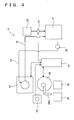
- a spin etching apparatus 10 has a spin etching section 12 where spin etching is performed on a wafer.
- Reference numeral 14 designates an etching solution circulating tank circulating an etching solution.
- the etching solution is fed to the spin etching section 12 by way of an etching solution feed line 16 for the etching solution circulating tank.
- the etching solution used in the spin etching section 12 is recovered to the etching solution circulating tank 14 by way of an etching solution recovery line 18.
- Reference numeral 20 designates an etching solution circulating pump provided in the etching solution feed line 16 and is used in feeding the etching solution to the spin etching section 12 from the etching solution circulating tank 14.
- Reference numeral 22 designates an additional etching solution tank storing a new etching solution and is connected to the etching solution circulating tank 14 by way of an etching solution adding pump 24. If the need arises, the new etching solution may be added to the etching solution circulating tank 14.
- Reference numeral 26 designates a weight measuring section, which measures weight of a wafer before and after etching the wafer in the spin etching section.
- Reference numeral 28 designates a handling mechanism section disposed adjacent to the spin etching section and having a robot hand section 28a, which transfers a wafer accommodated in a loading cassette 30 to the weight measuring section 26 to measure the weight.
- the handling mechanism section 28 functions not only to feed a wafer, the weight of which has been measured before the etching to the spin etching section 12, but also to transfer the etched wafer to the weight measuring section 26 from the spin etching section to measure the weight after the etching, and the wafer the weight of which has been measured after the etching is transferred to an unloading cassette 32 to take out the wafer.
- Reference numeral 34 designates a control section constituted of a computer and others, which is electrically connected to the spin etching section 12, the weight measuring section 26, the handling mechanism section 28 and the etching solution adding pump 24, respectively, and exchanges signals therewith to perform necessary control thereof.
- the control section 34 exchanges signals with the handling mechanism section 28 to drive the robot hand section 28a of the handling mechanism section 28 for transferring a wafer from the loading cassette 30 to the weight measuring section 26, from the weight measuring section 26 to the spin etching section 12, from the spin etching section 12 to the weight measuring section 26 and from the weight measuring section 26 to the unloading cassette 32.
- the control section 34 exchanges signals with the weight measuring section 26 to control weight measuring operation on a wafer in the weight measuring section 26, and to receive weight data signals from the weight measuring section 26.
- the control section 34 exchanges with the spin etching section 12 to control etching operation (an etching time, a rinse time, a drying time and others).
- an etching rate is calculated from an etching time and a difference between weight of the wafer before and after etching.
- the control section 34 has a function for comparing the calculated etching rate with a predetermined initial value to decide whether or not the calculated etching rate falls within an allowable range.
- the contact section 34 gives an etching solution adding signal to the etching solution adding pump 24 to add a given quantity of an etching solution to the etching solution circulating tank 14 so as to return an etching rate to a value in the vicinity of an initial value.
- etching treatment can be performed by using the same construction as the above-mentioned etching apparatus with the exception that the loading cassette 30 or the unloading cassette 32 are replaced with a dummy wafer, holding table.
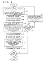
- a process control method in spin etching of the present invention There are two ways of methods for controlling an etching amount in the present invention. One is a method for controlling an etching stock removal of a wafer to a given value ( FIG. 1 ) and the other is a method for controlling weight of a finished wafer to a given value ( FIG. 2 ).
- wafers to be subjected to spin etching are prepared and set in a loading cassette 30.
- a first step, step 102 one wafer is taken out from the loading cassette 30 (a first step, step 102).
- the wafer is transferred to a weight measuring section 26 with a robot hand section 28a to measure the weight W 1 of the wafer before etching (a second step, step 104).
- the etching rate R is, to be concrete, an initial value R 0 of an etching solution to be used, an etching rate R 1 of the etching solution after etching or an etching rate R 2 of the etching solution into which an additional etching solution has been added.
- the wafer is transferred to the spin etching section 12 with the robot hand section 28a, is subjected to spin etching only for the calculated etching time To, and thereafter is rinsed and dried in given conditions.
- the spin etching treatment is shown as collectively including the spin etching, the rinsing and drying treatment (a fourth step, step 108).
- the wafer subjected to the spin etching treatment is transferred to the weight measuring section 26 with the robot hand section 28a to measure weight W 2 of the wafer after etching (a fifth step, step 110).
- the etched wafer is accommodated into the unloading cassette 32 with the robot hand section 28a (a seventh step, step 114).
- the control section 34 determines whether or not the calculated etching rate R 1 falls within a predetermined allowable range for an etching rate (an eighth step, step 118). If it is decided in the eighth step that a calculated etching rate R 1 falls within the allowable range (YES), a new next wafer is subjected to a process from the first step to the seventh step. On the other hand, it is decided in the eighth step that the calculated etching rate R1 falls outside the allowable range (NO), an additional etching solution (a new etching solution) is added into the etching solution stored in the etching solution circulating tank 14 and the etching rate R 1 thereof is restored to a value R 2 in the vicinity of the initial value R 0 (a ninth step, step 120).
- the new next wafer is subjected to the process from the first step to the seventh step.
- the etching rate R 2 is, as described above, measured in the confirmation treatment for an etching rate and thus obtained etching rate R 2 is used as an etching rate R in the equation (1).
- a termination deciding step step 116 is provided between the seventh step (step 114) and the eighth step (step 118) and if next etching is performed, the eighth step (step 118) is conducted, while if next etching is not performed, the operation is terminated.
- the etching rate to be concrete, indicates an initial value R 0 of an etching solution to be used, an etching rate R 1 of the etching solution after etching or an etching rate R 2 of the etching solution into which an additional etching solution has been added.
- the wafer is transferred to the spin etching section 12 with the robot hand section 28a, is subjected to spin etching only for the calculated etching time T, and thereafter is rinsed and dried in given conditions.
- the spin etching treatment is shown as collectively including the spin etching, the rinsing and drying treatment (a fifth step, step 108).
- the wafer subjected to the spin etching treatment is transferred to the weight measuring section 26 with the robot hand section 28a to measure weight W 2 of the wafer after etching (a sixth step, step 110).
- the etched wafer is accommodated into the unloading cassette 32 with the robot hand section 28a (an eight step, step 114).
- etching rate R 1 It is decided in the control section 34 whether or not the calculated etching rate R 1 falls within a predetermined allowable range for an etching rate (a ninth step, step 118). If it is decided in the ninth step that the calculated etching rate R 1 falls within the allowable range (YES), a new next wafer is subjected to a process from the first step to the eighth step.
- the calculated etching rate R 1 falls outside the allowable range (NO)
- an additional etching solution (a new etching solution) is added into an etching solution stored in the etching solution circulating tank 14 and the etching rate R 1 is restored to an etching rate R 2 in the vicinity of an initial value R 0 (a tenth step, step 120).
- a new next wafer is subjected to a process from the first step to the eighth step.
- the etching rate R 2 is, as described above, measured in etching rate confirmation treatment (step 100) and the etching rate R 2 is used as the etching rate R in the equation (4).
- a termination deciding step (step 116) is provided between the eighth step (step 114) and the ninth step (step 118) and if next etching is performed, the ninth step is conducted (step 118), while if next etching is not performed, the operation is terminated.
- An etching solution used in a method of the present invention can be a mixed acid solution consisting of four components [a 50% solution of hydrofluoric acid (15 wt %) + a 60% solution of phosphoric acid (25 wt %) + a 70% solution of nitric acid (35 wt %) and a 95% solution of sulfuric acid (25 wt % )], and like.
- a 50% solution of hydrofluoric acid and the like may be usable.
- a dummy wafer is prepared and set on the dummy wafer holding table.
- One dummy wafer is, as shown in Fig. 3 , is taken out from the dummy wafer holding table (a first step, step 200).
- the dummy wafer is transferred to the weight measuring section 26 with the robot hand section 28a to measure weight D 1 of the wafer before etching (a second step, step 202).
- the dummy wafer is transferred to the spin etching section 12 with the robot hand section 28a, is subjected to spin etching only for a given time to, and thereafter is rinsed and dried in given conditions.
- the above etching time to may be appropriately set to a value on the order in the range of 10 sec to 100 sec.
- the spin etching treatment is shown as collectively including the spin etching, the rinsing and drying treatment (a third step, step 204).
- the wafer subjected to the spin etching treatment is transferred to the weight measuring section 26 with the robot hand section 28a (a fourth step, step 206) to measure weight D 2 of the wafer after etching (a fifth step, step 208).
- the etched dummy wafer is transferred to the dummy wafer holding table with the robot hand 28
- an eighth step, step 214 It is decided in the control section 34 whether or not the weight D 2 of the dummy wafer after etching falls within in a defined range. If it is decided in the eighth step that the weight D 2 of the dummy wafer falls within a defined range (YES), confirmation treatment for an etching rate is terminated. On the other hand, if it is decided in the eighth step that the weight D 2 of the dummy wafer falls outside the defined range (NO), the control section 34 outputs an exchange request signal (a ninth step, step 216). If an exchange request signal is output, the used dummy wafer is not suited for further use, so a new dummy wafer is used at the next measurement time.
- the calculated etching rate r 0 may be used as an initial value R 0 and if an additional etching solution is added, the calculated etching rate r 0 may be used as an etching rate R 2 in the vicinity of an initial value R 0 .
- Ten pieces of 8-inch silicon wafers were spin etched one wafer at a time using a spin etching apparatus (MSE-2000, manufactured by Mimasu Semiconductor Industry CO.,LTD).
- An etching solution was 20 Kg of a mixed acid solution consisting of four components [a 50% solution of hydrofluoric acid (15 wt %) + a 60% solution of phosphoric acid (25 wt %) + a 70% solution of nitric acid (35 wt %) and a 95% solution of sulfuric acid (25 wt % )].
- An etching rate of the etching solution was measured using a dummy wafer according to the confirmation treatment for an etching rate shown in Fig. 3 .
- the obtained value of the etching rate was 1.560 (g/min).
- a target etching amount was set to 20 ⁇ m (1.444 g).
- the ten pieces of the silicon wafers were subjected to spin etching one wafer at a time using the etching solution at a temperature of 25°C ⁇ 1°C for a fixed time of 64 sec. There were measured an etching amount (g) and an etching rate (g/min) for each spin etched wafer and the results thereof were shown in Table 1 and FIG. 5 . As is apparent from the results of Table 1 and FIG.
- a process of the first step (step 102) to the seventh step (step 114) shown in the flowchart of FIG. 1 was repeated 10 times to spin etch the ten pieces of the wafers.
- an etching rate R 1 in the eighth step (step 118) was decided to fall within the allowable range and no additional etching solution was added.
- An etching amount (g), an etching rate (g/min) and an etching time (sec) were measured on each of the spin etched wafers. The results of the measurement were shown in Table 2 and FIG. 6 . As shown in Table 2 and FIG.
- the wafers were spin etched under condition that an etching amount (an etching stock removal) of each wafer was controlled to a constant value (20 ⁇ m: 1.444 g). Since an additional etching solution (a 50% solution of hydrofluoric acid) is added for supplement at the starting stage, the etching rate confirmation treatment step (step 100) of FIG. 1 was performed using a dummy wafer. The etching rate of the etching solution into which the additional etching solution was added for supplement was increased to 1.668 (g/min). Thereafter, a process of the first step (step 102) to the seventh step (step 114) of the flowchart shown in FIG. 1 was repeated 10 times to spin etch the ten pieces of the wafers.
- an etching amount an etching stock removal
- the additional etching solution was not added during the 10-time etching treatment.
- An etching amount (g), an etching rate g/min) and an etching time (sec) were measured on each of the spin etched wafers and the results there were shown in Table 3 and FIG. 7 .
- Table 3 and FIG. 7 it was found that if an etching rate decreased, a corresponding etching time increased automatically, from which an etching amount can be controlled to an almost constant value.
- an etching rate of the etching solution after the tenth wafer was spin etched was 1.523 (g/min).
- the wafer No. 0 in Table 3 is a dummy wafer. Table 3 Wafer Nos.
- an etching rate of the etching solution after the tenth wafer was spin etched was 1.305 (g/min).
- the wafer No. 0 in Table 3 is a dummy wafer.
- Table 4 Wafer Nos. 0 1 2 3 4 5 6 7 8 9 10 Weight before etching 50.72 48.53 48.59 47.67 49.77 49.75 49.75 49.78 49.81 49.79 49.81 Weight after etching 49.46 47.02 47.01 47.01 47.05 47.04 47.03 47.05 47.04 47.04 47.06
- Etching rate (g/min) 1.512 1.492 1.483 1.461 1.434 1.413 1.398 1.373 1.353 1.334 1.305 Etching time (sec) 50.0 60.7 62.3 26.4 110.8 112.1 113.7 116.2 119.6 120.5 123.1
Landscapes
- Engineering & Computer Science (AREA)
- Manufacturing & Machinery (AREA)
- Computer Hardware Design (AREA)
- Microelectronics & Electronic Packaging (AREA)
- Power Engineering (AREA)
- Physics & Mathematics (AREA)
- Plasma & Fusion (AREA)
- Condensed Matter Physics & Semiconductors (AREA)
- General Physics & Mathematics (AREA)
- Weting (AREA)
- Cleaning Or Drying Semiconductors (AREA)
Description
- The present invention relates to a novel process control method in spin etching, for example, for an etching amount and an etching solution.
- In fabrication of devices in recent years, there has been encountered a situation where wet etching treatment for a wafer with a spin etching apparatus is many times employed for purposes to increase a mechanical strength and to improve electric and thermal characteristics of a chip. In wet etching, with increase in the number of wafers processed therein, an etching rate is reduced since circulation use of an etching solution is common. The most important control item in the wet etching is control of a wafer thickness after the etching treatment. The thickness control is preferably conducted using a method for measuring a wafer thickness directly in light of its purpose. There arise cases, however, where patterning has been applied and electrodes have been formed on almost all wafers when a thickness of a wafer is measured, and further where a tape or a glass substrate is adhered on a wafer in order to protect the patterned surface thereof. A method for measuring a thickness with a good precision in such various conditions is very difficult to be conducted or requires a very expensive measuring instrument.
- Document
JP-H-01309332 - The treating time T=(etching depth)/(etching rate) is computed, and the etching rate Y is determined using the previously stored relationship Y=A+BX, wherein A and B are constants and X is the quantity of dissolved silicon. Document
US 2002/072235 A1 discloses an etching solution containing at least hydrofluoric acid, nitric acid and hexafluorosilicic acid wherein the concentration of hexafluorosilicic acid is not less than 10% by weight based on the weight of the etching solution. The etching speed is determined as follows: The etch amount is expressed by the weight difference of the silicon wafer between before and after the etching. The etching speed is calculated by dividing the etch amount by the time during which the silicon wafer is immersed in the mixed acid solution. - Document
US 2002/142619 A1 discloses a process for etching a silicon wafer by oxidizing silicon with permanganate ions and stripping the silicon oxide with hydrofluoric acid, in the presence of a non-oxidizable acid and typically a surfactant. - In a preferred embodiment in that document, the etching process provides a means to precisely control the amount of silicon removed from the wafer surface because the etching reagents are added in stoichiometric amounts, and these amounts are not maintained at a constant composition throughout the etching process. In examples, the result is reported in terms of weight difference.
- The present invention has been made in light of such circumstances in conventional technology and an object of the present invention is to provide a process control method in spin etching capable of realizing uniformity in etching amount in etching treatment for even wafers each having various conditions, and achieving uniformity of thickness values among etched wafers.
- The point of the present invention resides in that when spin etching a wafer weight control of the wafer is performed as a method for controlling an etching amount of the wafer to a given value. The method for controlling the etching amount of the wafer is divided to two ways; one is to control a stock removal by etching to a given value and the other is to control weight of the finished wafer to a given value.
- The method for process control in spin etching of the present invention (a method for controlling a stock removal from a wafer by etching to a given value) comprises:
- (a) a first step of taking out one wafer from a loading cassette;
- (b) a second step of measuring a weight W1 of the wafer before etching;
- (c) a third step of calculating an etching time T0 with the following equation (1):

- (d) a fourth step of etching the wafer for the calculated time T0;
- (e) a fifth step of measuring a weight W2 of the wafer after etching;
- (f) a sixth step of calculating the etching rate R1 of the etching solution after etching with the following equation (2):

- (g) a seventh step of accommodating the etched wafer; and
- (h) an eighth step of determining whether or not the etching rate R1 of the etching solution after etching falls within a predetermined allowable range,
- (a) a first step of taking out one wafer from a dummy wafer holding table;
- (b) a second step of measuring a weight D1 of the dummy wafer before etching;
- (c) a third step of etching the dummy wafer for a given time t0 ;
- (d) a fourth step of measuring a weight D2 of the dummy wafer after etching;
- (e) a fifth step of calculating an etching rate r0 of the etching solution after etching with the following equation (6):

- (g) a sixth step of transferring the etched dummy wafer to the dummy wafer holding table; and
- (h) an seventh step of determining whether or not the weight D2 of the etched dummy wafer falls within a defined range;
- According to the method of the present invention, spin etching can be continuously conducted such that an etching amount V is controlled to a given value.
- Incidentally, when an exchange request signal for the used dummy wafer is issued, a different dummy wafer is used in the next measurement since the used dummy wafer is not suitable for further use.
- In the method of the present invention, weight control of a wafer is performed as a method for controlling an etching amount of the wafer to a given value. Roughly speaking, the following procedure is performed therefore.
- The weight of a wafer before etching is measured in units of 1/1000 g, followed by predetermined etching treatment in a spin etching section. Thereafter, the weight of the wafer is again measured in units of 1/1000 g after rinsing and drying treatment of the wafer, and then an actual etching amount is calculated from a difference between weight before and after etching of the wafer, confirming an etching rate each time etching to thereby control an etching time.
- A first one wafer etched in a new etching solution or in an etching solution after an additional etching solution is added is a dummy wafer and etching treatment is performed on the dummy wafer for a fixed time to confirm an etching rate. In etching treatment of a second wafer and those subsequent thereto, a change in etching rate of the etching solution is calculated from a change in weight of the wafer before and after etching to conduct time control and to correct a shortage of etching corresponding to reduction in the etching rate. Since correction only with extension of the etching time results in extension of a treatment time and reduction of productivity, the maximum value of a time correction or the limit value of an etching rate is determined. When the value of the time correction equals to the above maximum value or more, or the value of the etching rate equals to the above limit value or more, an additional etching solution is added into a circulating system of the etching solution in order to recover an etching rate.
- In the method for controlling an etching amount and an etching solution in spin etching as described, in step (c) the third step may further comprise determining an etching amount V0 with the following equation (3):

-
-
FIG. 1 is a flowchart showing an example step sequence according to a first aspect of the method of the present invention. -
FIG. 2 is a flowchart showing another example step sequence according to a second aspect of the method of the present invention. -
FIG. 3 is a flowchart showing the step sequence of confirmation treatment for an etching rate comprised in the method of the present invention. -
FIG. 4 is a block diagram showing a spin etching apparatus according to a comparative example not being part of the present invention. -
FIG. 5 is a graph showing changing characteristics of etching to etched wafers in Example 1. -
FIG. 6 is a graph showing changes in etching amount, etching rate and etching time to etched wafers in Example 1. -
FIG. 7 is a graph showing changes in etching amount, etching rate and etching time to etched wafers in Example 2 -
FIG. 8 is a graph showing changes in weight after etching and etching rate to etched wafers in Example 3. - Description will be given of embodiments of the present invention below based on the accompanying drawings, and it is needless to say that the embodiments shown in figures are presented by way of illustration and various modification or variations can be implemented as far as not departing from the technical concept of the present invention.
- First of all, description is presented of a spin etching apparatus of according to a comparative example not being part of the present invention using
FIG. 4 . InFIG. 4 , aspin etching apparatus 10 according to the comparative example has aspin etching section 12 where spin etching is performed on a wafer.Reference numeral 14 designates an etching solution circulating tank circulating an etching solution. The etching solution is fed to thespin etching section 12 by way of an etchingsolution feed line 16 for the etching solution circulating tank. The etching solution used in thespin etching section 12 is recovered to the etchingsolution circulating tank 14 by way of an etchingsolution recovery line 18.Reference numeral 20 designates an etching solution circulating pump provided in the etchingsolution feed line 16 and is used in feeding the etching solution to thespin etching section 12 from the etchingsolution circulating tank 14.Reference numeral 22 designates an additional etching solution tank storing a new etching solution and is connected to the etchingsolution circulating tank 14 by way of an etchingsolution adding pump 24. If the need arises, the new etching solution may be added to the etchingsolution circulating tank 14. -
Reference numeral 26 designates a weight measuring section, which measures weight of a wafer before and after etching the wafer in the spin etching section.Reference numeral 28 designates a handling mechanism section disposed adjacent to the spin etching section and having arobot hand section 28a, which transfers a wafer accommodated in aloading cassette 30 to theweight measuring section 26 to measure the weight. And thehandling mechanism section 28 functions not only to feed a wafer, the weight of which has been measured before the etching to thespin etching section 12, but also to transfer the etched wafer to theweight measuring section 26 from the spin etching section to measure the weight after the etching, and the wafer the weight of which has been measured after the etching is transferred to an unloadingcassette 32 to take out the wafer. -
Reference numeral 34 designates a control section constituted of a computer and others, which is electrically connected to thespin etching section 12, theweight measuring section 26, thehandling mechanism section 28 and the etchingsolution adding pump 24, respectively, and exchanges signals therewith to perform necessary control thereof. Thecontrol section 34 exchanges signals with thehandling mechanism section 28 to drive therobot hand section 28a of thehandling mechanism section 28 for transferring a wafer from the loadingcassette 30 to theweight measuring section 26, from theweight measuring section 26 to thespin etching section 12, from thespin etching section 12 to theweight measuring section 26 and from theweight measuring section 26 to the unloadingcassette 32. Thecontrol section 34 exchanges signals with theweight measuring section 26 to control weight measuring operation on a wafer in theweight measuring section 26, and to receive weight data signals from theweight measuring section 26. - The
control section 34 exchanges with thespin etching section 12 to control etching operation (an etching time, a rinse time, a drying time and others). In thecontrol section 34, an etching rate is calculated from an etching time and a difference between weight of the wafer before and after etching. Thecontrol section 34 has a function for comparing the calculated etching rate with a predetermined initial value to decide whether or not the calculated etching rate falls within an allowable range. If the etching rate falls outside the allowable range, thecontact section 34 gives an etching solution adding signal to the etchingsolution adding pump 24 to add a given quantity of an etching solution to the etchingsolution circulating tank 14 so as to return an etching rate to a value in the vicinity of an initial value. Incidentally, in confirmation treatment using a dummy wafer for an etching rate thereon described later a dummy wafer is etched, and in this case, etching treatment can be performed by using the same construction as the above-mentioned etching apparatus with the exception that theloading cassette 30 or the unloadingcassette 32 are replaced with a dummy wafer, holding table. - Subsequent to this, description will be given of a process control method in spin etching of the present invention. There are two ways of methods for controlling an etching amount in the present invention. One is a method for controlling an etching stock removal of a wafer to a given value (
FIG. 1 ) and the other is a method for controlling weight of a finished wafer to a given value (FIG. 2 ). - Description will be given of the first way of a process control method in a spin etching of the present invention with a spin etching apparatus, the apparatus according to the comparative example, using
FIG. 1 (a method for controlling an etching stock removal of a wafer to a given value). First of all, confirmation treatment is performed for an etching rate R of an etching solution to be used (a preliminary step, step 100). In the confirmation treatment for an etching rate, which will be detailed later, there is measured for confirmation an initial value R0 of an etching solution to be used or an etching rate R2 of the etching solution into which an additional etching solution has been added. On the other hand, wafers to be subjected to spin etching are prepared and set in aloading cassette 30. As shown inFIG. 1 , one wafer is taken out from the loading cassette 30 (a first step, step 102). The wafer is transferred to aweight measuring section 26 with arobot hand section 28a to measure the weight W1 of the wafer before etching (a second step, step 104). - An etching time T0 for the wafer is calculated using the following equation(1) in the
control section 34 from the etching rate R of the etching solution to be used and a target etching amount V0 (a third step, step 106):
spin etching section 12 with therobot hand section 28a, is subjected to spin etching only for the calculated etching time To, and thereafter is rinsed and dried in given conditions. In the flowchart ofFIG. 1 , the spin etching treatment is shown as collectively including the spin etching, the rinsing and drying treatment (a fourth step, step 108). - The wafer subjected to the spin etching treatment is transferred to the
weight measuring section 26 with therobot hand section 28a to measure weight W2 of the wafer after etching (a fifth step, step 110). An etching rate R1 of the etching solution after etching is calculated using the following equation (2) in thecontrol section 34 from the weight W1 of the wafer before etching, the weight W2 of the wafer after etching and the etching time T0 (a sixth step, step 112):
cassette 32 with therobot hand section 28a (a seventh step, step 114). - It is decided in the
control section 34 whether or not the calculated etching rate R1 falls within a predetermined allowable range for an etching rate (an eighth step, step 118). If it is decided in the eighth step that a calculated etching rate R1 falls within the allowable range (YES), a new next wafer is subjected to a process from the first step to the seventh step. On the other hand, it is decided in the eighth step that the calculated etching rate R1 falls outside the allowable range (NO), an additional etching solution (a new etching solution) is added into the etching solution stored in the etchingsolution circulating tank 14 and the etching rate R1 thereof is restored to a value R2 in the vicinity of the initial value R0 (a ninth step, step 120). Then, the new next wafer is subjected to the process from the first step to the seventh step. In this case, the etching rate R2 is, as described above, measured in the confirmation treatment for an etching rate and thus obtained etching rate R2 is used as an etching rate R in the equation (1). Incidentally, it is preferable that, as shown inFIG. 1 , a termination deciding step (step 116) is provided between the seventh step (step 114) and the eighth step (step 118) and if next etching is performed, the eighth step (step 118) is conducted, while if next etching is not performed, the operation is terminated. - Description will be given, then, of the second way of a process control method of a spin etching of the present invention with a spin etching apparatus, the apparatus according to the comparative example, using
FIG. 2 (a method for controlling weight of a finished wafer to a given value). First of all, in a similar way to that in the process ofFig. 1 , confirmation treatment is performed for an etching rate R of an etching solution to be used (a preliminary step, step 100). On the other hand, wafers to be subjected to spin etching are prepared and set in theloading cassette 30. As shownFIG. 2 , one wafer is taken out from the loading cassette 30 (a first step, step 102). The wafer is transferred to theweight measuring section 26 with therobot hand section 28a to measure the weight W1 of the wafer before etching (a second step, step 104). - An etching amount V on the wafer is calculated using the following equation (3) in the
control section 34 from the weight W1 of the wafer before etching and weight W0 of the finished wafer (a third step, step 105):
- An etching time T for the wafer is calculated in the
control section 34 using the following equation (4) from an etching rate R of an etching solution to be used and the etching amount V (a fourth step, step 106):
spin etching section 12 with therobot hand section 28a, is subjected to spin etching only for the calculated etching time T, and thereafter is rinsed and dried in given conditions. In the flowchart ofFIG. 2 , the spin etching treatment is shown as collectively including the spin etching, the rinsing and drying treatment (a fifth step, step 108). - The wafer subjected to the spin etching treatment is transferred to the
weight measuring section 26 with therobot hand section 28a to measure weight W2 of the wafer after etching (a sixth step, step 110). An etching rate R1 of the etching solution after etching is calculated in thecontrol section 34 using the following equation (5) from weight W1 of the wafer before etching, weight W2 of the wafer after etching and an etching time T (a seventh step, step 112):
cassette 32 with therobot hand section 28a (an eight step, step 114). - It is decided in the
control section 34 whether or not the calculated etching rate R1 falls within a predetermined allowable range for an etching rate (a ninth step, step 118). If it is decided in the ninth step that the calculated etching rate R1 falls within the allowable range (YES), a new next wafer is subjected to a process from the first step to the eighth step. On other hand, if it is decided in the ninth step that the calculated etching rate R1 falls outside the allowable range (NO), an additional etching solution (a new etching solution) is added into an etching solution stored in the etchingsolution circulating tank 14 and the etching rate R1 is restored to an etching rate R2 in the vicinity of an initial value R0 (a tenth step, step 120). Then, a new next wafer is subjected to a process from the first step to the eighth step. In this case, the etching rate R2 is, as described above, measured in etching rate confirmation treatment (step 100) and the etching rate R2 is used as the etching rate R in the equation (4). Incidentally, it is preferable that, as shown inFIG. 2 , a termination deciding step (step 116) is provided between the eighth step (step 114) and the ninth step (step 118) and if next etching is performed, the ninth step is conducted (step 118), while if next etching is not performed, the operation is terminated. - An etching solution used in a method of the present invention can be a mixed acid solution consisting of four components [a 50% solution of hydrofluoric acid (15 wt %) + a 60% solution of phosphoric acid (25 wt %) + a 70% solution of nitric acid (35 wt %) and a 95% solution of sulfuric acid (25 wt % )], and like. As an additional etching solution, a 50% solution of hydrofluoric acid and the like may be usable.
- Description will be given of confirmation treatment for an etching rate of an etching solution to be used (that is, an initial value R0 of an etching solution to be used or an etching rate R2 of the etching solution into which an additional etching solution has been added) using
FIG. 3 . First of all, a dummy wafer is prepared and set on the dummy wafer holding table. One dummy wafer is, as shown inFig. 3 , is taken out from the dummy wafer holding table (a first step, step 200). The dummy wafer is transferred to theweight measuring section 26 with therobot hand section 28a to measure weight D1 of the wafer before etching (a second step, step 202). - The dummy wafer is transferred to the
spin etching section 12 with therobot hand section 28a, is subjected to spin etching only for a given time to, and thereafter is rinsed and dried in given conditions. The above etching time to may be appropriately set to a value on the order in the range of 10 sec to 100 sec. In the flowchart ofFIG. 3 , the spin etching treatment is shown as collectively including the spin etching, the rinsing and drying treatment (a third step, step 204). - The wafer subjected to the spin etching treatment is transferred to the
weight measuring section 26 with therobot hand section 28a (a fourth step, step 206) to measure weight D2 of the wafer after etching (a fifth step, step 208). An etching rate r0 of the etching solution is calculated in thecontrol section 34 using the following equation (6) from the weight D1 of the dummy wafer before etching, the weight D2 of the dummy wafer after etching and the etching time to (a sixth step, step 210):
robot hand 28a (a seventh step, step 212). - It is decided in the
control section 34 whether or not the weight D2 of the dummy wafer after etching falls within in a defined range (an eighth step, step 214). If it is decided in the eighth step that the weight D2 of the dummy wafer falls within a defined range (YES), confirmation treatment for an etching rate is terminated. On the other hand, if it is decided in the eighth step that the weight D2 of the dummy wafer falls outside the defined range (NO), thecontrol section 34 outputs an exchange request signal (a ninth step, step 216). If an exchange request signal is output, the used dummy wafer is not suited for further use, so a new dummy wafer is used at the next measurement time. Incidentally, if an etching solution is a starting etching solution, the calculated etching rate r0 may be used as an initial value R0 and if an additional etching solution is added, the calculated etching rate r0 may be used as an etching rate R2 in the vicinity of an initial value R0. - More concrete description will be given of the present invention showing examples below and it is needless to say that the examples are presented by way of illustration and should not be construed by way of limitation.
- An experiment was conducted on changes in an etching rate of an etching solution. Ten pieces of 8-inch silicon wafers were spin etched one wafer at a time using a spin etching apparatus (MSE-2000, manufactured by Mimasu Semiconductor Industry CO.,LTD). An etching solution was 20 Kg of a mixed acid solution consisting of four components [a 50% solution of hydrofluoric acid (15 wt %) + a 60% solution of phosphoric acid (25 wt %) + a 70% solution of nitric acid (35 wt %) and a 95% solution of sulfuric acid (25 wt % )]. An etching rate of the etching solution was measured using a dummy wafer according to the confirmation treatment for an etching rate shown in
Fig. 3 . The obtained value of the etching rate was 1.560 (g/min). A target etching amount was set to 20 µm (1.444 g). The ten pieces of the silicon wafers were subjected to spin etching one wafer at a time using the etching solution at a temperature of 25°C ± 1°C for a fixed time of 64 sec. There were measured an etching amount (g) and an etching rate (g/min) for each spin etched wafer and the results thereof were shown in Table 1 andFIG. 5 . As is apparent from the results of Table 1 andFIG. 5 , it was confirmed that an etching rate decreased with increase in the number of spin etched wafers (wherein an etching rate of the etching solution after the tenth wafer was spin etched was 1.356 (g/min)), and an etching amount decreased in proportion to reduction in etching rate. The wafer No. 0 in Table 1 is a dummy wafer.Table 1 Wafer Nos. 0 1 2 3 4 5 6 7 8 9 10 Weight before etching 38.18 51.81 52.71 52.71 53.8 53.81 53.81 53.8 53.82 53.79 53.81 Weight after etching 36.88 50.52 51.43 51.46 52.57 52.59 52.61 52.63 52.66 52.65 52.68 Etching amount (g) 1.30 1.29 1.28 1.25 1.23 1.22 1.2 1.17 1.16 1.14 1.13 Etching rate (g/min) 1.560 1.548 1.536 1.500 1.476 1.464 1.440 1.404 1.392 1.368 1.356 - An experiment was conducted for controlling an etching stock removal of a wafer to a constant value (without adding an additional etching solution). Ten pieces of 8-inch silicon wafers were spin etched one wafer at a time using a spin etching apparatus (MSE-2000, manufactured by Mimasu Semiconductor Industry CO.,LTD.). In this experiment, the etching solution used in Empirical Example 1 was used consecutively as it was. An initial etching rate of the etching solution was 1.356 (g/min). The wafers were spin etched under condition that an etching amount (an etching stock removal) of each wafer was controlled to a constant value (20 µm: 1.444 g). That is, a process of the first step (step 102) to the seventh step (step 114) shown in the flowchart of
FIG. 1 was repeated 10 times to spin etch the ten pieces of the wafers. In this example, an etching rate R1 in the eighth step (step 118) was decided to fall within the allowable range and no additional etching solution was added. An etching amount (g), an etching rate (g/min) and an etching time (sec) were measured on each of the spin etched wafers. The results of the measurement were shown in Table 2 andFIG. 6 . As shown in Table 2 andFIG. 6 , it was found that if an etching rate decreased, a corresponding etching time increased automatically, from which an etching amount can be controlled to an almost constant value. In this Example, an etching rate of the etching solution after the tenth wafer was spin etched was 1.356 (g/min).Table 2 Wafer Nos. 1 2 3 4 5 6 7 8 9 10 Weight before etching 51.44 50.53 51.42 52.59 52.59 52.62 52.62 52.65 52.63 52.67 Weight after etching 50.01 49.09 49.99 51.18 51.18 51.19 51.2 51.21 51.21 51.24 Etching amount (g) 1.43 1.44 1.43 1.41 1.41 1.43 1.42 1.44 1.42 1.43 Etching rate (g/min) 1.347 1.347 1.337 1.309 1.282 1.273 1.256 1.256 1.238 1.229 Etching time (sec) 63.7 64.2 64.2 64.6 66.0 67.4 67.9 68.8 68.8 69.8 - There was conducted an experiment in which an etching stock removal of a wafer is controlled to a constant value (addition of an additional solution). Ten pieces of 8-inch silicon wafers were spin etched one wafer at a time using a spin etching apparatus (MSE-2000, manufactured by Mimasu Semiconductor Industry CO.,LTD.). In this experiment, there was used an etching solution which was prepared by adding 0.5 Kg of a 50% solution of hydrofluoric acid into the etching solution that had been used in Example 1 (an etching rate of the used etching solution was decreased to 1.229 (g/min)). In the same way as in Example 1, the wafers were spin etched under condition that an etching amount (an etching stock removal) of each wafer was controlled to a constant value (20 µm: 1.444 g). Since an additional etching solution (a 50% solution of hydrofluoric acid) is added for supplement at the starting stage, the etching rate confirmation treatment step (step 100) of
FIG. 1 was performed using a dummy wafer. The etching rate of the etching solution into which the additional etching solution was added for supplement was increased to 1.668 (g/min). Thereafter, a process of the first step (step 102) to the seventh step (step 114) of the flowchart shown inFIG. 1 was repeated 10 times to spin etch the ten pieces of the wafers. The additional etching solution was not added during the 10-time etching treatment. An etching amount (g), an etching rate g/min) and an etching time (sec) were measured on each of the spin etched wafers and the results there were shown in Table 3 andFIG. 7 . As shown in Table 3 andFIG. 7 , it was found that if an etching rate decreased, a corresponding etching time increased automatically, from which an etching amount can be controlled to an almost constant value. In this Example, an etching rate of the etching solution after the tenth wafer was spin etched was 1.523 (g/min). The wafer No. 0 in Table 3 is a dummy wafer.Table 3 Wafer Nos. 0 1 2 3 4 5 6 7 8 9 10 Weight before etching 52.11 49.09 50.01 49.99 51.18 51.19 51.18 51.2 51.21 51.21 51.24 Weight after etching 50.72 47.67 48.59 48.54 49.77 49.74 49.76 49.77 49.8 49.78 49.81 Etching quantities (g) 1.39 1.42 1.42 1.45 1.41 1.45 1.42 1.43 1.41 1.43 1.43 Etching rates (g/min) 1.668 1.645 1.622 1.633 1.599 1.610 1.588 1.577 1.544 1.533 1.523 Etching times (sec) 50.0 51.8 52.5 53.3 52.9 54.0 53.7 54.4 54.8 56.0 56.3 - There was conducted an experiment in which finished weight of a wafer is controlled to a constant value (without addition of an additional solution). Ten pieces of 8-inch silicon wafers were spin etched one wafer at a time using a spin etching apparatus (MSE-2000, manufactured by Mimasu Semiconductor Industry CO.,LTD.). In this experiment, the etching solution used in Example 2 was used consecutively as it was. An initial etching rate of the etching solution was 1.512 (g/min). The wafers were spin etched under condition that finished weight of each wafer was controlled to a constant value (47.0 g). That is, a process of the first step (step 102) to the seventh step (step 114) shown in the flowchart of
FIG. 2 was repeated 10 times to spin etch the ten pieces of the wafers. In the 10-time etching treatment, no additional etching solution was added. An etching amount (g), an etching rate (g/min) and an etching time (sec) were measured on each of the spin etched wafers. The results of the measurement were shown in Table 4 andFIG. 8 (translation of the etching time into a graphic form is omitted). As shown in Table 4 andFIG.8 , it was found that if an etching rate decreased, a corresponding etching time increased automatically, from which weight of the wafer after etching can be controlled to an almost constant value. In this Example, an etching rate of the etching solution after the tenth wafer was spin etched was 1.305 (g/min). The wafer No. 0 in Table 3 is a dummy wafer.Table 4 Wafer Nos. 0 1 2 3 4 5 6 7 8 9 10 Weight before etching 50.72 48.53 48.59 47.67 49.77 49.75 49.75 49.78 49.81 49.79 49.81 Weight after etching 49.46 47.02 47.01 47.01 47.05 47.04 47.03 47.05 47.04 47.04 47.06 Etching amount (g) 1.26 1.51 1.58 0.66 2.72 2.71 2.72 2.73 2.77 2.75 2.75 Etching rate (g/min) 1.512 1.492 1.483 1.461 1.434 1.413 1.398 1.373 1.353 1.334 1.305 Etching time (sec) 50.0 60.7 62.3 26.4 110.8 112.1 113.7 116.2 119.6 120.5 123.1 - According to the present invention, there is exerted an effect that uniformity in etching amount in etching treatment can be realized even for wafers each having various conditions, and uniformity of thickness values among etched wafers can also be achieved.
wherein confirmation treatment is performed for the initial value R0 of the etching rate of the starting etching solution and/or the etching rate R2 of the etching solution which has been restored to a value in the vicinity of the initial value by adding an additional etching solution into the used etching solution, wherein the confirmation treatment for the etching rate comprises:
Claims (2)
- A method for controlling an etching amount and an etching solution in spin etching, comprising:(a) a first step (102) of taking out one wafer from a loading cassette (30);(b) a second step (104) of measuring a weight W1 of the wafer before etching;(c) a third step (106) of calculating an etching time T0 with the following equation (1):
 (d) a fourth step (108) of etching the wafer for the calculated time T0;(e) a fifth step (110) of measuring a weight W2 of the wafer after etching;(f) a sixth step (112) of calculating the etching rate R1 of the etching solution after etching with the following equation (2):
 (g) a seventh step (114) of accommodating the etched wafer; and(h) an eighth step (118) of determining whether or not the etching rate R1 of the etching solution after etching falls within a predetermined allowable range, wherein when it is decided in the eighth step (118) that the etching rate R1 falls within the predetermined allowable range, the process from the first step (102) to the seventh step (114) is performed on a wafer to be processed in the next order, or when it is decided in the eighth step (118) that the etching rate R1 falls outside the predetermined allowable range, there is performed a ninth step (120) of adding an additional etching solution into the etching solution to restore the etching rate R1 to the etching rate R2 in the vicinity of the initial value R0, and thereafter the process from the first step (102) to the seventh step (114) is performed on a wafer to be processed in the next order;wherein confirmation treatment (100) is performed for the initial value R0 of the etching rate of the starting etching solution and/or the etching rate R2 of the etching solution which has been restored to a value in the vicinity of the initial value by adding an additional etching solution into the used etching solution;
wherein the confirmation treatment (100) for the etching rate comprises:(i) a first step (200) of taking out one wafer from a dummy wafer holding table;(ii) a second step (202) of measuring a weight D1 of the dummy wafer before etching;(iii) a third step (204) of etching the dummy wafer for a given time t0 ;(iv) a fourth step (208) of measuring a weight D2 of the dummy wafer after etching;(v) a fifth step (210) of calculating an etching rate r0 of the etching solution after etching with the following equation (6): (vi) a sixth step (212) of transferring the etched dummy wafer to the dummy wafer holding table; and(vii) a seventh step (214) of determining whether or not the weight D2 of the etched dummy wafer falls within a defined range; wherein when it is decided in the seventh step (214) that weight D2 of the dummy wafer falls within the defined range, the confirmation treatment for the etching rate is terminated, or when it is decided in the seventh step (214) that the weight of the dummy wafer D2 falls outside the defined range, there is performed an eighth step (216) of generating an exchange request signal for the used dummy wafer, and thereafter the confirmation treatment (100) for the etching rate is terminated.
 - The method for controlling an etching amount and an etching solution in spin etching according to claim 1:wherein in step (c) the third step further comprises determining (105) the etching amount V0 with the following equation (3):
 wherein V0 indicates the etching amount, in g, W1 is the weight, in g, of the wafer before etching, and W0 is a weight of a finished wafer, that is a target weight, in g, of the wafer after etching.
Applications Claiming Priority (1)
| Application Number | Priority Date | Filing Date | Title |
|---|---|---|---|
| PCT/JP2004/003817 WO2005091346A1 (en) | 2004-03-22 | 2004-03-22 | Schedule control method in spin etching and spin etching system |
Publications (3)
| Publication Number | Publication Date |
|---|---|
| EP1729332A1 EP1729332A1 (en) | 2006-12-06 |
| EP1729332A4 EP1729332A4 (en) | 2010-09-15 |
| EP1729332B1 true EP1729332B1 (en) | 2016-10-12 |
Family
ID=34993963
Family Applications (1)
| Application Number | Title | Priority Date | Filing Date |
|---|---|---|---|
| EP04722390.4A Expired - Fee Related EP1729332B1 (en) | 2004-03-22 | 2004-03-22 | Schedule control method in spin etching |
Country Status (7)
| Country | Link |
|---|---|
| US (2) | US7659212B2 (en) |
| EP (1) | EP1729332B1 (en) |
| JP (1) | JP4364242B2 (en) |
| KR (1) | KR101010532B1 (en) |
| CN (1) | CN100508133C (en) |
| TW (1) | TW200539267A (en) |
| WO (1) | WO2005091346A1 (en) |
Families Citing this family (19)
| Publication number | Priority date | Publication date | Assignee | Title |
|---|---|---|---|---|
| JP2008177329A (en) * | 2007-01-18 | 2008-07-31 | Mitsubishi Electric Corp | Wet etching method |
| JP4978548B2 (en) * | 2008-04-25 | 2012-07-18 | 三菱化学株式会社 | Etching method and method for manufacturing substrate for semiconductor device |
| CN101651098B (en) * | 2009-06-12 | 2012-10-17 | 上海宏力半导体制造有限公司 | Etching method |
| CN102569019B (en) * | 2010-12-17 | 2014-06-04 | 无锡华润上华半导体有限公司 | Shallow trench isolation forming method |
| TWI441272B (en) * | 2011-09-26 | 2014-06-11 | Lextar Electronics Croportion | A method for monitoring etching process |
| JP6163434B2 (en) | 2014-01-16 | 2017-07-12 | 株式会社東芝 | Chemical treatment apparatus and chemical treatment method |
| US9478408B2 (en) | 2014-06-06 | 2016-10-25 | Lam Research Corporation | Systems and methods for removing particles from a substrate processing chamber using RF plasma cycling and purging |
| US10081869B2 (en) | 2014-06-10 | 2018-09-25 | Lam Research Corporation | Defect control in RF plasma substrate processing systems using DC bias voltage during movement of substrates |
| US10047438B2 (en) | 2014-06-10 | 2018-08-14 | Lam Research Corporation | Defect control and stability of DC bias in RF plasma-based substrate processing systems using molecular reactive purge gas |
| CN104332430B (en) * | 2014-09-04 | 2017-02-15 | 常州捷佳创精密机械有限公司 | Silicon chip online weighing control system and control method thereof |
| US10679862B2 (en) | 2016-04-21 | 2020-06-09 | Mimasu Semiconductor Industry Co., Ltd. | Contactless electric power supply mechanism and method for rotary table, and wafer rotating and holding device |
| WO2017204082A1 (en) | 2016-05-24 | 2017-11-30 | 三益半導体工業株式会社 | Wafer holding mechanism and method for rotary table and rotary wafer holding device |
| JP6837481B2 (en) | 2016-05-26 | 2021-03-03 | 三益半導体工業株式会社 | Wafer heating and holding mechanism and method for rotary table and wafer rotation holding device |
| CN106298573A (en) * | 2016-09-13 | 2017-01-04 | 冠礼控制科技(上海)有限公司 | The method of testing of rate of etch is improved by silicon chip spinning and oscillating mechanism |
| US11075218B2 (en) * | 2019-05-22 | 2021-07-27 | Sandisk Technologies Llc | Method of making a three-dimensional memory device using silicon nitride etching end point detection |
| CN113496886B (en) * | 2020-04-03 | 2022-10-25 | 重庆超硅半导体有限公司 | Method for controlling alkali corrosion removal amount of monocrystalline silicon wafer for integrated circuit |
| JP7153361B2 (en) * | 2020-04-18 | 2022-10-14 | 有限会社Nas技研 | Bulk etching method and bulk etching apparatus |
| CN111339693B (en) * | 2020-05-19 | 2020-10-13 | 深圳市乾行达科技有限公司 | Workpiece etching method and device and terminal equipment |
| CN115938929B (en) * | 2022-12-14 | 2023-11-03 | 湖北江城芯片中试服务有限公司 | Etching machine and control method thereof |
Citations (2)
| Publication number | Priority date | Publication date | Assignee | Title |
|---|---|---|---|---|
| US20020142619A1 (en) * | 2001-03-30 | 2002-10-03 | Memc Electronic Materials, Inc. | Solution composition and process for etching silicon |
| US20030121889A1 (en) * | 2000-05-01 | 2003-07-03 | Teruo Takahashi | Thickness measuring apparatus, thickness measuring method, and wet etching apparatus and wet etching method utilizing them |
Family Cites Families (13)
| Publication number | Priority date | Publication date | Assignee | Title |
|---|---|---|---|---|
| JPS61287124A (en) * | 1985-06-13 | 1986-12-17 | Oki Electric Ind Co Ltd | Method for processing chemical liquid for substrate and device therefor |
| AT389959B (en) * | 1987-11-09 | 1990-02-26 | Sez Semiconduct Equip Zubehoer | DEVICE FOR SETTING DISC-SHAPED OBJECTS, ESPECIALLY SILICONE DISC |
| JPH01236633A (en) * | 1988-03-16 | 1989-09-21 | Rohm Co Ltd | Etching end point detection |
| JPH01309332A (en) * | 1988-06-08 | 1989-12-13 | Toyo Electric Mfg Co Ltd | Automatic control apparatus for etching |
| KR0166831B1 (en) * | 1995-12-18 | 1999-02-01 | 문정환 | Cleaning apparatus and method of semiconductor wafer |
| KR100192489B1 (en) * | 1995-12-26 | 1999-06-15 | 구본준 | Method for measuring wet etch |
| US6221171B1 (en) * | 1996-06-04 | 2001-04-24 | Ebara Corporation | Method and apparatus for conveying a workpiece |
| DE19641070A1 (en) * | 1996-10-04 | 1998-04-09 | Wacker Siltronic Halbleitermat | Silicon wafer defects determining method for manufacture |
| JP4590700B2 (en) * | 2000-07-14 | 2010-12-01 | ソニー株式会社 | Substrate cleaning method and substrate cleaning apparatus |
| TW511180B (en) * | 2000-07-31 | 2002-11-21 | Mitsubishi Chem Corp | Mixed acid solution in etching process, process for producing the same, etching process using the same and process for producing semiconductor device |
| JP2003077838A (en) * | 2001-08-30 | 2003-03-14 | Toshiba Corp | Dry cleaning time determining system, dry cleaning method, and dry cleaning system of semiconductor- manufacturing apparatus, and manufacturing method of semiconductor device |
| JP2003215002A (en) * | 2002-01-17 | 2003-07-30 | Dainippon Screen Mfg Co Ltd | Apparatus and method for treating board |
| US6902647B2 (en) * | 2002-08-29 | 2005-06-07 | Asm International N.V. | Method of processing substrates with integrated weighing steps |
-
2004
- 2004-03-22 JP JP2006511101A patent/JP4364242B2/en not_active Expired - Lifetime
- 2004-03-22 US US10/586,873 patent/US7659212B2/en active Active
- 2004-03-22 EP EP04722390.4A patent/EP1729332B1/en not_active Expired - Fee Related
- 2004-03-22 KR KR1020067011345A patent/KR101010532B1/en active IP Right Grant
- 2004-03-22 CN CNB2004800414707A patent/CN100508133C/en not_active Expired - Lifetime
- 2004-03-22 WO PCT/JP2004/003817 patent/WO2005091346A1/en not_active Application Discontinuation
-
2005
- 2005-03-18 TW TW094108480A patent/TW200539267A/en unknown
-
2009
- 2009-12-01 US US12/628,603 patent/US20100101726A1/en not_active Abandoned
Patent Citations (2)
| Publication number | Priority date | Publication date | Assignee | Title |
|---|---|---|---|---|
| US20030121889A1 (en) * | 2000-05-01 | 2003-07-03 | Teruo Takahashi | Thickness measuring apparatus, thickness measuring method, and wet etching apparatus and wet etching method utilizing them |
| US20020142619A1 (en) * | 2001-03-30 | 2002-10-03 | Memc Electronic Materials, Inc. | Solution composition and process for etching silicon |
Also Published As
| Publication number | Publication date |
|---|---|
| US20100101726A1 (en) | 2010-04-29 |
| KR20060126990A (en) | 2006-12-11 |
| CN100508133C (en) | 2009-07-01 |
| TWI347631B (en) | 2011-08-21 |
| US7659212B2 (en) | 2010-02-09 |
| JPWO2005091346A1 (en) | 2008-02-07 |
| EP1729332A1 (en) | 2006-12-06 |
| US20080242101A1 (en) | 2008-10-02 |
| TW200539267A (en) | 2005-12-01 |
| WO2005091346A1 (en) | 2005-09-29 |
| KR101010532B1 (en) | 2011-01-24 |
| JP4364242B2 (en) | 2009-11-11 |
| EP1729332A4 (en) | 2010-09-15 |
| CN1914713A (en) | 2007-02-14 |
Similar Documents
| Publication | Publication Date | Title |
|---|---|---|
| EP1729332B1 (en) | Schedule control method in spin etching | |
| US5310457A (en) | Method of integrated circuit fabrication including selective etching of silicon and silicon compounds | |
| KR101243847B1 (en) | Method for etching cu/mo alloy film with etching capacity of etching solution improved | |
| US5472562A (en) | Method of etching silicon nitride | |
| KR102009250B1 (en) | Method for manufacturing display device and an etching solution composition for metal layer containing copper/metal oxide layer | |
| CN101399196B (en) | Coarsening processing method for backing side of wafer | |
| US6153014A (en) | Method of cleaning a silicon wafer using a standard cleaning solution | |
| KR20170068328A (en) | Etchant composition, and method for etching | |
| KR101723264B1 (en) | Method for setting substrate-treatment time, and storage medium | |
| US6663674B2 (en) | Method of handling a silicon wafer | |
| US7064085B2 (en) | Feed forward spacer width control in semiconductor manufacturing | |
| KR101173692B1 (en) | Solution for the selective removal of metal from aluminum substrates | |
| KR20130025612A (en) | An etching solution composition for oxide layer containing gallium | |
| EP1112591B1 (en) | Method and apparatus for wet-etching semiconductor wafers | |
| EP1149411A1 (en) | Method and apparatus for wet-etching semiconductor wafers | |
| JP2000144453A (en) | Etching system and etching method | |
| CN1118517A (en) | Process for treating semiconductor material with an acid-containing fluid | |
| KR20240031104A (en) | Substrate processing apparatus and substrate processing method | |
| WO2024004725A1 (en) | Substrate treatment apparatus and substrate treatment method | |
| JP2024033157A (en) | Substrate processing equipment and substrate processing method | |
| CN112908845A (en) | Optimized control method and system for initial etching rate of oxide film | |
| CN115516608A (en) | Method for manufacturing SOI wafer | |
| KR20020081923A (en) | Cleaning Method of Semiconductor Wafer | |
| EP0797243A2 (en) | Etching process for dielectric layers in semiconductor devices | |
| KR19990070081A (en) | Semiconductor metrology system and method for reducing wafer loading time |
Legal Events
| Date | Code | Title | Description |
|---|---|---|---|
| PUAI | Public reference made under article 153(3) epc to a published international application that has entered the european phase |
Free format text: ORIGINAL CODE: 0009012 |
|
| 17P | Request for examination filed |
Effective date: 20060829 |
|
| AK | Designated contracting states |
Kind code of ref document: A1 Designated state(s): DE FR GB |
|
| DAX | Request for extension of the european patent (deleted) | ||
| RBV | Designated contracting states (corrected) |
Designated state(s): DE FR GB |
|
| A4 | Supplementary search report drawn up and despatched |
Effective date: 20100816 |
|
| 17Q | First examination report despatched |
Effective date: 20101104 |
|
| REG | Reference to a national code |
Ref country code: DE Ref legal event code: R079 Ref document number: 602004050104 Country of ref document: DE Free format text: PREVIOUS MAIN CLASS: H01L0021306000 Ipc: H01L0021660000 |
|
| GRAP | Despatch of communication of intention to grant a patent |
Free format text: ORIGINAL CODE: EPIDOSNIGR1 |
|
| RIC1 | Information provided on ipc code assigned before grant |
Ipc: H01L 21/66 20060101AFI20160411BHEP Ipc: H01L 21/306 20060101ALI20160411BHEP |
|
| INTG | Intention to grant announced |
Effective date: 20160511 |
|
| GRAS | Grant fee paid |
Free format text: ORIGINAL CODE: EPIDOSNIGR3 |
|
| GRAA | (expected) grant |
Free format text: ORIGINAL CODE: 0009210 |
|
| AK | Designated contracting states |
Kind code of ref document: B1 Designated state(s): DE FR GB |
|
| REG | Reference to a national code |
Ref country code: GB Ref legal event code: FG4D |
|
| REG | Reference to a national code |
Ref country code: DE Ref legal event code: R096 Ref document number: 602004050104 Country of ref document: DE |
|
| REG | Reference to a national code |
Ref country code: FR Ref legal event code: PLFP Year of fee payment: 14 |
|
| REG | Reference to a national code |
Ref country code: DE Ref legal event code: R097 Ref document number: 602004050104 Country of ref document: DE |
|
| PLBE | No opposition filed within time limit |
Free format text: ORIGINAL CODE: 0009261 |
|
| STAA | Information on the status of an ep patent application or granted ep patent |
Free format text: STATUS: NO OPPOSITION FILED WITHIN TIME LIMIT |
|
| 26N | No opposition filed |
Effective date: 20170713 |
|
| REG | Reference to a national code |
Ref country code: FR Ref legal event code: PLFP Year of fee payment: 15 |
|
| PGFP | Annual fee paid to national office [announced via postgrant information from national office to epo] |
Ref country code: FR Payment date: 20190322 Year of fee payment: 16 Ref country code: GB Payment date: 20190320 Year of fee payment: 16 |
|
| PGFP | Annual fee paid to national office [announced via postgrant information from national office to epo] |
Ref country code: DE Payment date: 20200320 Year of fee payment: 17 |
|
| PG25 | Lapsed in a contracting state [announced via postgrant information from national office to epo] |
Ref country code: FR Free format text: LAPSE BECAUSE OF NON-PAYMENT OF DUE FEES Effective date: 20200331 |
|
| GBPC | Gb: european patent ceased through non-payment of renewal fee |
Effective date: 20200322 |
|
| PG25 | Lapsed in a contracting state [announced via postgrant information from national office to epo] |
Ref country code: GB Free format text: LAPSE BECAUSE OF NON-PAYMENT OF DUE FEES Effective date: 20200322 |
|
| REG | Reference to a national code |
Ref country code: DE Ref legal event code: R119 Ref document number: 602004050104 Country of ref document: DE |
|
| PG25 | Lapsed in a contracting state [announced via postgrant information from national office to epo] |
Ref country code: DE Free format text: LAPSE BECAUSE OF NON-PAYMENT OF DUE FEES Effective date: 20211001 |