EP1726922A2 - Abtastschaltung - Google Patents
Abtastschaltung Download PDFInfo
- Publication number
- EP1726922A2 EP1726922A2 EP06008606A EP06008606A EP1726922A2 EP 1726922 A2 EP1726922 A2 EP 1726922A2 EP 06008606 A EP06008606 A EP 06008606A EP 06008606 A EP06008606 A EP 06008606A EP 1726922 A2 EP1726922 A2 EP 1726922A2
- Authority
- EP
- European Patent Office
- Prior art keywords
- circuit according
- scanning circuit
- effect transistor
- signal
- field effect
- Prior art date
- Legal status (The legal status is an assumption and is not a legal conclusion. Google has not performed a legal analysis and makes no representation as to the accuracy of the status listed.)
- Granted
Links
- 230000005669 field effect Effects 0.000 claims abstract description 52
- 238000005070 sampling Methods 0.000 claims description 49
- 230000008878 coupling Effects 0.000 claims description 9
- 238000010168 coupling process Methods 0.000 claims description 9
- 238000005859 coupling reaction Methods 0.000 claims description 9
- 239000003990 capacitor Substances 0.000 claims description 8
- 230000000737 periodic effect Effects 0.000 claims description 5
- 238000010586 diagram Methods 0.000 description 3
- 238000005259 measurement Methods 0.000 description 3
- 238000000034 method Methods 0.000 description 3
- 238000006243 chemical reaction Methods 0.000 description 2
- 229910001218 Gallium arsenide Inorganic materials 0.000 description 1
- 230000001427 coherent effect Effects 0.000 description 1
- 230000001419 dependent effect Effects 0.000 description 1
- 238000001514 detection method Methods 0.000 description 1
- 238000000605 extraction Methods 0.000 description 1
- 238000001914 filtration Methods 0.000 description 1
- 230000004048 modification Effects 0.000 description 1
- 238000012986 modification Methods 0.000 description 1
- 230000005855 radiation Effects 0.000 description 1
- 230000001629 suppression Effects 0.000 description 1
Images


Classifications
-
- G—PHYSICS
- G01—MEASURING; TESTING
- G01R—MEASURING ELECTRIC VARIABLES; MEASURING MAGNETIC VARIABLES
- G01R19/00—Arrangements for measuring currents or voltages or for indicating presence or sign thereof
- G01R19/25—Arrangements for measuring currents or voltages or for indicating presence or sign thereof using digital measurement techniques
- G01R19/2506—Arrangements for conditioning or analysing measured signals, e.g. for indicating peak values ; Details concerning sampling, digitizing or waveform capturing
- G01R19/2509—Details concerning sampling, digitizing or waveform capturing
-
- G—PHYSICS
- G01—MEASURING; TESTING
- G01R—MEASURING ELECTRIC VARIABLES; MEASURING MAGNETIC VARIABLES
- G01R19/00—Arrangements for measuring currents or voltages or for indicating presence or sign thereof
- G01R19/0046—Arrangements for measuring currents or voltages or for indicating presence or sign thereof characterised by a specific application or detail not covered by any other subgroup of G01R19/00
- G01R19/0053—Noise discrimination; Analog sampling; Measuring transients
-
- G—PHYSICS
- G01—MEASURING; TESTING
- G01S—RADIO DIRECTION-FINDING; RADIO NAVIGATION; DETERMINING DISTANCE OR VELOCITY BY USE OF RADIO WAVES; LOCATING OR PRESENCE-DETECTING BY USE OF THE REFLECTION OR RERADIATION OF RADIO WAVES; ANALOGOUS ARRANGEMENTS USING OTHER WAVES
- G01S7/00—Details of systems according to groups G01S13/00, G01S15/00, G01S17/00
- G01S7/02—Details of systems according to groups G01S13/00, G01S15/00, G01S17/00 of systems according to group G01S13/00
- G01S7/28—Details of pulse systems
- G01S7/285—Receivers
- G01S7/292—Extracting wanted echo-signals
Definitions
- the invention relates to a sampling circuit for the sequential sampling of a broadband, periodic input signal, wherein a non-linear component is provided, to which a pulse-shaped sampling signal is supplied, whereby the sampling is activated, so that an output signal is generated.
- the detection of a broadband signal or a rapidly changing signal waveform can not be realized by direct real-time sampling or only with great technical effort.
- a typical application is the level measurement by means of a pulse radar, the technical difficulty is to measure the duration of the radar signal very accurately. For a distance measurement accuracy of 1 mm, an accuracy of the time measurement of about 6 ps is required.
- One possible alternative to direct real-time sampling is sequential sampling. Sequential sampling uses a much lower sampling rate, but is limited to use with periodic signals only. In contrast to real-time sampling, only one sample per signal period is recorded. Subsequently, the fast signal to be scanned is reconstructed from a plurality of individual sampling points. Since this sampling method results in frequency conversion of the input signal, this process can also be interpreted as harmonic mixing.
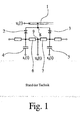
- FIG. 1 A conventional realization of a sampling circuit is shown in FIG.
- An input signal to be sampled is fed via a transmitting and receiving line 1 to two antiparallel-arranged switching diodes 2, 3.
- the two anti-parallel arranged switching diodes 2, 3 are operated in the idle state by a respective applied DC bias initially in the reverse direction.
- a pulse-shaped sampling signal s 1 (t) and an inverse sampling signal s 2 (t) switch the switching diodes 2, 3 so that the distance between the supply of the input signal u c (t) to be sampled and two switching diodes 2 , 3 respectively downstream sampling capacitors 4, 5 become low-resistance for a short time.
- Disadvantages of this conventional solution include the extreme demands on the phase and amplitude characteristics of the two mutually inverse scanning signals, which are required for a functioning balancing. To ensure the balance, the two scanning signals must be identical in magnitude and at the same time have rotated through exactly 180 ° phases, which makes the generation of these signals can be correspondingly expensive or makes the operation of the circuit prone to component tolerances.
- this object is achieved in that a field effect transistor is provided as a non-linear component.
- a field effect transistor is used to activate the sampling, that is to detect the input signal to be sampled when the pulse-shaped sampling signal is present, in order to produce the output signal as a sampled signal. It is true that field effect transistors have an inherent decoupling between the gate and drain, so that with a suitable wiring of the field effect transistor, the scanning signal neither in the signal path still speaking in the intermediate frequency path. Another advantage of a sampling circuit with a field effect transistor is the inherent noise balance since the signal applied to the gate is not rectified.
- the supply of the input signal takes place at the drain contact of the field effect transistor.
- the supply of the scanning signal is provided at the gate contact of the field effect transistor.
- the decoupling of the output signal is also provided at the drain contact of the field effect transistor.
- the supply of the input signal is separated from the coupling-out of the output signal by means of a filter arrangement.
- a filter arrangement Preferably, a high-pass filter is used on the side of the feed and / or a low-pass filter is used on the side of the feed-out.
- a multi-stage LC filter with magnetically shielded inductors is particularly preferred.
- the extraction of the output signal takes place at the source contact of the field effect transistor.
- the drain contact of the field effect transistor is DC-decoupled via a capacitance.
- the input signal is supplied to the field effect transistor via a transmitting and receiving line, in which an II attenuator is inserted.
- a filter arrangement is further provided on the side of the coupling out, most preferably in the form of an RC filter chain.
- a storage capacitor is preferably provided on the side of the coupling.
- an additional field effect transistor connected as a "dummy" can furthermore be provided.
- the drain contact of the additional field effect transistor is loaded with an impedance, which is preferably identical to the load impedance, by which other field effect transistor is loaded at the drain contact through the signal path.
- the two field effect transistors are supplied with the same scanning signal.
- the two field effect transistors are driven with the same gate bias voltage.
- sampling circuits each comprise Schottky contact GaAs junction field effect transistors which are operated passively, ie without the specification of a drain-source voltage. In addition to very good large signal characteristics can be achieved in this way an absolute stability of the circuit.
- the actual sampling or frequency conversion of a broadband input signal u c (t) to a narrow-band intermediate frequency signal u s (t) is achieved by the modulation of the non-linear voltage-dependent drain-source channel resistance by means of a pulse-shaped sampling signal s (t).
- a sampling circuit Via a transmitting and receiving line 10, the sampling circuit is supplied with the input signal to be scanned.
- the coupling of the input signal to be scanned takes place via the drain contact 11 of a field effect transistor 12.
- a scanning signal s (t) is applied to the gate 13 of the field effect transistor 12.
- the sampling signal In combination with an applied DC bias voltage U DC , the sampling signal periodically controls the channel resistance of the drain-source path, thus determining the operating point for the input signal u c (t) to be sampled.
- the DC operating point of the field effect transistor 12 typically becomes chosen on the voltage applied to the gate contact 13 bias voltage such that in combination with the supplied via a capacitor 14 sampling signal, the modulation of the channel between the closed and open channel.
- the time average impedance of the drain-source path and thus the output impedance of the circuit can be determined by the choice of DC bias and the polarity of the pulses of the scanning signal in combination with the channel doping of the field effect transistor 12, the time average impedance of the drain-source path and thus the output impedance of the circuit. If, for example, the gate 13 of the field-effect transistor 12 is negatively biased at an n-doped channel and the polarity of the scanning signal is selected to be positive, the drain-source path is only during the duration of the short pulses of the scanning signal low resistance and thus high impedance over time, in this case in the range of a few kilohms.
- a slightly positive DC bias in combination with negative pulses of the sample signal causes on average a relatively low impedance of the drain-source path in the range of less ohms.
- the polarity selection of the control of the circuit and the associated determination of the output impedance does not directly affect the performance of the circuit, but rather depends on the intended application.
- a realization with a low-impedance output impedance allows, for example, despite a possibly required DC-coupled coupling of the intermediate frequency signal, an approximately DC-free output signal, since no memory charge can build up on the low-resistance channel resistance, which would then be superimposed on the intermediate frequency signal as a DC component.
- the feed of the sampled input signal u c (t) and the coupling of the sampled signal, ie the output signal u s (t) take place at the drain contact 11 of the field effect transistor 12.
- the two signals are separated by a filter assembly 15. Namely, a high-pass filter 16 is provided on the input signal side, and a low-pass filter 17 is provided on the output side of the sampled signal.
- a filter assembly 15 Namely, a high-pass filter 16 is provided on the input signal side, and a low-pass filter 17 is provided on the output side of the sampled signal.
- a multi-stage LC filter which has only magnetically shielded inductors, in order to prevent a possible magnetic coupling at this circuit point.
- a sampling circuit according to a second preferred embodiment of the invention will now be apparent.
- the filtering measures required to separate the input signal from the output signal can be further simplified. While the drain contact 11 of the field effect transistor 12 without a filter is located directly in the transmit and receive paths, the tap of the output signal at the source contacts 18 of the field effect transistor 12 is provided.
- the send and receive line incorporated an II attenuator 19, which serves to improve the input matching of the circuit.
- the bias voltage at the gate 13 of the field effect transistor 12 is selected to be negative and the polarity of the pulses of the sampling signal is positive, then the channel resistance of the drain-source path becomes low for the duration of a pulse of the sampling signal, so that a to the source Contact 18 connected storage capacitor 20 is charged to a fraction of the instantaneous voltage of u c (t).
- the channel is high impedance, so that the intermediate frequency tap is isolated from the input signal u c (t) to be sampled.
- a simple RC filter chain 21 is advantageous that these are insensitive to magnetic and electrical radiation in contrast to LC filters, so that the Coupling of non-coherent signals is prevented.
- a sampling circuit according to a third preferred embodiment of the invention is described, it is virtually an extension of the apparent from Fig. 3 circuit according to the second preferred embodiment of the invention, wherein an additional field effect transistor 22 is provided.
- This circuit with two field effect transistors 12, 22 is composed of two identically constructed individual circuits, wherein the output signal of the entire circuit from the difference of Eisenfreqtienzsignale of the two individual circuits is formed, for which purpose a differential amplifier 27 is provided.
- the upper individual circuit of the entire circuit according to the third preferred embodiment of the invention of FIG. 4 corresponds to the previously described circuit of FIG. 3.
- the lower-circuit field effect transistor 22 is connected as a "dummy". That is, the drain contact 23 of the additional field effect transistor 22 is loaded with an impedance 24 which is identical to the load impedance through which the field effect transistor 12 at the drain contact 11 is loaded by the signal path.
- both circuits with the same scanning signal and the same Gate bias voltage controlled are also identical, so that the pulses of the scanning signal pass over the two gates 13, 25 of the field-effect transistors 12, 22 and are terminated without reflection with a terminating impedance 26.
- the DC components in the intermediate frequency signals u s1 (t) and u s2 (t) of each circuit are also identical, so that the difference u s1 (t) - u s2 (t) gives the DC-free intermediate frequency signal u s (t).
Landscapes
- Physics & Mathematics (AREA)
- General Physics & Mathematics (AREA)
- Networks Using Active Elements (AREA)
- Electronic Switches (AREA)
- Control Of Indicators Other Than Cathode Ray Tubes (AREA)
Abstract
Description
- Die Erfindung betrifft eine Abtastschaltung zur sequentiellen Abtastung eines breitbandigen, periodischen Eingangssignals, wobei ein nichtlineares Bauelement vorgesehen ist, dem ein impulsförmiges Abtastsignal zugeführt wird, wodurch die Abtastung aktiviert wird, so daß ein Ausgangssignal erzeugt wird.
- Die Erfassung eines breitbandigen Signals bzw. eines sich zeitlich schnell ändernden Signalverlaufs läßt sich mittels direkter Echtzeitabtastung gar nicht oder nur unter sehr großem technischen Aufwand realisieren. Ein typischer Anwendungsfall ist die Füllstandsmessung mittels eines Puls-Radars, wobei die technische Schwierigkeit darin liegt, die Laufzeit des Radar-Signals sehr genau zu messen. Für eine Abstandsmeßgenauigkeit von 1 mm ist nämlich eine Genauigkeit der Zeitmessung von etwa 6 ps erforderlich. Eine mögliche Alternative zur direkten Echtzeitabtastung stellt eine sequentielle Abtastung dar. Die sequentielle Abtastung kommt mit einer deutlich geringeren Abtastrate aus, ist jedoch ausschließlich auf die Anwendung bei periodischen Signalen beschränkt. Im Gegensatz zur Echtzeitabtastung wird dabei pro Signalperiode nur ein Abtastwert aufgenommen. Anschließend wird das schnelle, abzutastende Signal aus einer Vielzahl einzelner Abtastpunkte rekonstruiert. Da dieses Abtastverfahren eine Frequenzumsetzung des Eingangssignals zur Folge hat, läßt sich dieser Vorgang auch als Oberwellenmischung deuten.
- Eine herkömmliche Realisierung einer Abtast- bzw. Sampling-Schaltung ist in Fig. 1 dargestellt. Ein abzutastendes Eingangssignal wird über eine Sende- und Empfangsleitung 1 auf zwei antiparallel angeordnete Schaltdioden 2, 3 geführt. Die beiden antiparallel angeordneten Schaltdioden 2, 3 werden im Ruhezustand durch eine jeweils angelegte DC-Vorspannung zunächst in Sperrichtung betrieben. Während des eigentlichen Abtastvorgangs schalten ein impulsförmiges Abtastsignal s1 (t) und ein dazu inverses Abtastsignal s2 (t) die Schaltdioden 2, 3 leitend, so daß die Strecke zwischen der Einspeisung des abzutastenden Eingangssignals uc (t) und zwei den Schaltdioden 2, 3 jeweils nachgeschalteten Abtastkondensatoren 4, 5 für eine kurze Zeit niederohmig werden. Der Ladungsanteil auf den Abtastkondensatoren 4, 5, der von den impulsförmigen Abtastimpulsen herrührt, kann sich über Widerstände 6, 7 entladen. Unter der Voraussetzung, daß die Abtastkondensatoren 4, 5 zwischen zwei Abtastvorgängen vollständig entladen werden, ergeben sich die Abtastpunkte des abgetasteten Eingangssignals prinzipiell aus der über den Abtastkondensatoren 4, 5 anstehenden mittleren Spannung us (t). Gilt zwischen den beiden Abtastsignalen der Zusammenhang s1 (t) = -s2 (t), so lassen sich die Knoten 8, 9 bezüglich dieser Signale als virtuelle Massepunkte ansehen, Folglich heben sich im Idealfall die Abtastsignale an diesen Knoten 8, 9 gegenseitig auf, so daß ein Übersprechen der Abtastsignale in den Zwischenfrequenzpfad und den Signalpfad unterbunden wird, womit eine Balancierung der Schaltung erzielt wird.
- Nachteilig bei dieser herkömmlichen Lösung sind unter anderem die extremen Anforderungen an den Phasen- und Amplitudenverlauf der beiden zueinander inversen Abtastsignale wie sie für eine funktionierende Balancierung erforderlich sind. Für die Gewährleistung der Balancierung müssen die beiden Abtastsignale dem Betrag nach identisch sein und gleichzeitig um genau 180° gedrehte Phasen aufweisen, was die Erzeugung dieser Signale entsprechend aufwendig werden läßt bzw. die Funktionsweise der Schaltung anfällig für Bauteiltoleranzen macht.
- Ausgehend von dieser Problematik ist es die Aufgabe der Erfindung, eine derartige Schaltung anzugeben, die kostengünstig, technisch robust und vielseitig sowie einfach anwendbar ist.
- Ausgehend von der eingangs beschriebenen Abtastschaltung zur sequentiellen Abtastung eines breitbandigen, periodischen Eingangssignals ist diese Aufgabe dadurch gelöst, daß als nichtlineares Bauelement ein Feldeffekttransistor vorgesehen ist.
- Erfindungsgemäß wird also ein Feldeffekttransistor verwendet, um die Abtastung zu aktivieren, also bei anliegendem impulsförmigen Abtastsignal das abzutastende Eingangssignal zu erfassen, um damit als abgetastetes Signal das Ausgangssignal zu erzeugen. Dabei gilt, daß Feldeffekttransistoren eine inhärente Entkopplung zwischen Gate und Drain aufweisen, so daß bei geeigneter Beschaltung des Feldeffekttransistors das Abtastsignal weder in den Signalpfad noch in den Zwischenfrequenzpfad einspricht. Ein weiterer Vorteil einer Abtastschaltung mit einem Feldeffekttransistor liegt in der inhärenten Rauschbalancierung, da das am Gate anliegende Signal nicht gleichgerichtet wird.
- Insgesamt erhält man also eine inhärente Entkopplung von Ansteuersignal und Ausgangssignal bei inhärenter Rauschbalancierung der Abtastschaltung. Durch die Auswahl unterschiedlicher Typen von Feldeffekttransistoren (n-Kanal/p-Kanal) ergeben sich weitere Freiheitsgrade bezüglich der Polarität der unipolaren Ablastimpulse und der Realisierung unterschiedlicher Ausgangsimpedanzen für das abgetastete Eingangssignal.
- Grundsätzlich gibt es verschiedene Möglichkeiten der Einspeisung des Eingangssignals bzw. des Abtastsignals. Gemäß einer bevorzugten Weiterbildung der Erfindung ist jedoch vorgesehen, daß die Einspeisung des Eingangssignals am Drain-Kontakt des Feldeffekttransistors erfolgt. Gemäß einer bevorzugten Weiterbildung der Erfindung ist ferner vorgesehen, daß die Einspeisung des Abtastsignals am Gate-Kontakt des Feldeffekttransistors vorgesehen ist.
- Gemäß einer bevorzugten Weiterbildung der Erfindung ist ferner die Auskopplung des Ausgangssignals am Drain-Kontakt des Feldeffekttransistors vorgesehen. Dabei ist vorzugsweise insbesondere weiterhin vorgesehen, daß die Einspeisung des Eingangssignals von der Auskopplung des Ausgangssignals mittels einer Filteranordnung getrennt ist. Vorzugsweise wird dabei auf der Seite der Einspeisung ein Hochpaßfilter und/oder auf der Seite der Auskopplung ein Tiefpaßfilter verwendet. Ganz besonders bevorzugt ist dabei ein mehrstufiger LC-Filter mit magnetisch abgeschirmten Induktivitäten.
- Gemäß einer anderen bevorzugten Weiterbildung der Erfindung ist vorgesehen, daß die Auskopplung des Ausgangssignals am Source-Kontak des Feldeffekttransistors erfolgt. Vorzugsweise ist dabei der Drain-Kontakt des Feldeffekttransistors über eine Kapazität DC-entkoppelt. Außerdem ist dabei vorzugsweise vorgesehen, daß das Eingangssignal dem Feldeffekttransistor über eine Sende- und Empfangsleitung zugeführt wird, in die ein II-Dämpfungsglied eingefügt ist. Vorzugsweise ist ferner auf der Seite der Auskopplung eine Filteranordnung vorgesehen, ganz besonders bevorzugt in Form einer RC-Filterkette. Schließlich ist auf der Seite der Auskopplung vorzugsweise noch ein Speicherkondensator vorgesehen.
- Bei der zuletzt beschriebenen bevorzugten Weiterbildung der Erfindung kann weiterhin ein zusätzlicher, als "Dummy" beschalteter Feldeffekttransistor vorgesehen sein. Damit erhält man eine Schaltungsstruktur, die eine Erweiterung der zuvor beschriebenen Schaltung darstellt. Quasi handelt es sich um zwei identisch aufgebaute Einzelschaltungen mit je einem Feldeffekttransistor, wobei das Ausgangssignal der gesamten Schaltung aus der Differenz der Zwischenfrequenzsignale der beiden Einzelschaltungen gebildet wird. Während die eine Einzelschaltung so ausgebildet ist und betrieben wird, wie zuvor beschrieben, ist der Feldeffekttransistor der zusätzlichen Einzelschaltung als "Dummy" beschaltet: Der Drain-Kontakt des zusätzlichen Feldeffekttransistors ist mit einer Impedanz belastet, die vorzugsweise identisch der Lastimpedanz ist, durch die der andere Feldeffekttransistor am Drain-Kontakt durch den Signalpfad belastet ist. Vorzugsweise kann weiterhin vorgesehen sein, daß die beiden Feldeffekttransistoren mit demselben Abtastsignal gespeist werden. Außerdem ist vorzugsweise vorgesehen, daß die beiden Feldeffekttransistoren mit derselben Gate-Vorspannung angesteuert werden.
- Im einzelnen gibt es nun eine Vielzahl von Möglichkeiten, die erfindungsgemäße Abtastschaltung zur sequentiellen Abtastung eines breitbandigen, periodischen Eingangssignals auszugestalten und weiterzubilden. Dazu wird auf die dem Patentanspruch 1 nachgeordneten Patentansprüche sowie auf die nachfolgende detaillierte Beschreibung bevorzugter Ausführungsbeispiele der Erfindung unter Bezugnahme auf die Zeichnung verwiesen. In der Zeichnung zeigt
- Fig. 1
- ein Prinzipschaltbild einer auf antiparallel geschalteten Dioden basierenden herkömmlichen Abtastschaltung,
- Fig. 2
- ein Prinzipschaltbild einer Abtastschaltung gemäß einem ersten bevorzugten Ausführungsbeispiel der Erfindung,
- Fig. 3
- ein Prinzipschaltbild einer Abtastschaltung gemäß einem zweiten bevorzugten Ausführungsbeispiel der Erfindung und
- Fig. 4
- eine Abtastschaltung gemäß einem dritten bevorzugten Ausführungsbeispiel der Erfindung.
- Die im folgenden beschriebenen Abtastschaltungen gemäß bevorzugter Ausführungsbeispiele der Erfindung weisen jeweils GaAs-Sperrschicht-Feldeffekttransistoren mit Schottky-Kontakt auf, die passiv, d. h. ohne die Vorgabe einer Drain-Source-Spannung, betrieben werden. Neben sehr guten Großsignaleigenschaften läßt sich auf diesem Weg eine absolute Stabilität der Schaltung erzielen. Die eigentliche Abtastung bzw, die Frequenzumsetzung eines breitbandigen Eingangssignals uc (t) auf ein schmalbandiges Zwischenfrequenzsignal us (t) erfolg durch die Aussteuerung des nichtlinearen spannungsabhängigen Drain-Source-Kanalwiderstands mittels eines impulsförmigen Abtastsignals s (t).
- Aus Fig. 1 ist nun eine Abtastschaltung gemäß einem ersten bevorzugten Ausführungsbeispiel der Erfindung ersichtlich. Über eine Sende- und Empfangsleitung 10 wird der Abtastschaltung das abzutastende Eingangssignal zugeführt. Die Einkopplung des abzutastenden Eingangssignals erfolgt über den Drain-Kontakt 11 eines Feldeffekttransistors 12. Ein Abtastsignal s (t) wird auf das Gate 13 des Feldeffekttransistors 12 gegeben. In Kombination mit einer angelegten DC-Vorspannung UDC steuert das Abtastsignal damit periodisch den Kanalwiderstand der Drain-Source-Strecke, womit der Arbeitspunkt für das abzutastende Eingangssignal uc (t) bestimmt wird, Der DC-Arbeitspunkt des Feldeffekttransistors 12 wird in der Regel über die am Gate-Kontakt 13 angelegte Vorspannung derart gewählt, daß in Kombination mit dem über einen Kondensator 14 zugeführten Abtastsignal die Aussteuerung des Kanals zwischen geschlossenem und offenem Kanal erfolgt.
- Weiterhin läßt sich durch die Wahl der DC-Vorspannung und der Polarität der Impulse des Abtastsignals in Kombination mit der Kanaldotierung des Feldeffekttransistors 12 die zeitlich mittlere Impedanz der Drain-Source-Strecke und damit die Ausgangsimpedanz der Schaltung bestimmen. Wird das Gate 13 des Feldeffekttransistors 12 bei einem n-dotierten Kanal beispielsweise negativ vorgespannt und wird die Polarität des Abtastsignals positiv gewählt, so ist die Drain-Source-Strecke nur während der Dauer der kurzen Impulse des Abtastsignals niederohmig und damit im zeitlichen Mittel hochohmig, und zwar vorliegend im Bereich von einigen Kiloohm.
- Andererseits bewirkt eine leicht positive DC-Vorspannung in Kombination mit negativen Impulsen des Abtastsignals im zeitlichen Mittel eine relativ niederohmige Impedanz der Drain-Source-Strecke im Bereich weniger Ohm. Die Polaritätswahl der Ansteuerung der Schaltung und die damit verbundene Bestimmung der Ausgangsimpedanz nimmt nicht unmittelbar Einfluß auf die Leistungsfähigkeit der Schaltung, sondern richtet sich vielmehr nach der vorgesehenen Anwendung. Eine Realisierung mit einer niederohmigen Ausgangsimpedanz ermöglicht beispielsweise trotz einer eventuell geforderten DC-gekoppelten Auskopplung des Zwischenfrequenzsignals ein annähernd DC-freies Ausgangssignal, da sich über dem niederohmigen Kanalwiderstand keine Speicherladung aufbauen kann, die anschließend dem Zwischenfrequenzsignal als DC-Anteil überlagert wäre.
- Die Einspeisung des abzutastenden Eingangssignals uc (t) und die Auskopplung des abgetasteten Signals, also des Ausgangssignals us (t) erfolgen am Drain-Kontakt 11 des Feldeffekttransistors 12. Dabei sind die beiden Signale durch eine Filteranordnung 15 voneinander getrennt. Auf der Seite der Einspeisung des Eingangssignals ist nämlich ein Hochpaßfilter 16 und auf der Seite der Auskopplung des abgetasteten Signals ist ein Tiefpaßfilter 17 vorgesehen. Hier bietet sich die Verwendung eines mehrstufigen LC-Filters an, der ausschließlich magnetisch abgeschirmte Induktivitäten aufweist, um eine eventuelle magnetische Einkopplung an diesem Schaltungspunkt zu unterbinden.
- Aus Fig. 3 ist nun eine Abtastschaltung gemäß einem zweiten bevorzugten Ausführungsbeispiel der Erfindung ersichtlich. Durch eine geringe Modifikation der Struktur der Schaltung im Vergleich zum ersten bevorzugten Auführungsbeispiel der Erfindung lassen sich die erforderlichen Filtermaßnahmen zur Trennung des Eingangssignals vom Ausgangssignal weiter vereinfachen. Während der Drain-Kontakt 11 des Feldeffekttransistors 12 ohne einen Filter direkt im Sende- und Empfangspfad liegt, ist der Abgriff des Ausgangssignals am Source-Kontakte 18 des Feldeffekttransistors 12 vorgesehen. Bei diesem bevorzugten Ausführungsbeispiel der Erfindung ist in die Sende- und Empfangsleitung ein II-Dämpfungsglied 19 eingebaut, das der Verbesserung der Eingangsanpassung der Schaltung dient.
- Werden, wie zuvor beschrieben, die Vorspannung am Gate 13 des Feldeffekttransistors 12 negativ gewählt und die Polarität der Impulse des Abtastsignals positiv, so wird für die Dauer eines Impulses des Abtastsignals der Kanalwiderstand der Drain-Source-Strecke niederohmig, so daß ein an den Source-Kontakt 18 angeschlossener Speicherkondensator 20 auf einen Bruchteil der Momentanspannung von uc (t) aufgeladen wird. Für die restliche Zeit einer Abtastperiode ist der Kanal hochohmig, so daß der Zwischenfrequenzabgriff vom abzutastenden Eingangssignal uc (t) isoliert ist. Zur weiteren Unterdrükkung der dennoch dem Zwischenfrequenzsignal am Source-Kontakt überlagerten geringen höherfrequenten Signalanteile dient eine einfache RC-Filterkette 21. Bei RC-Filtern ist dabei vorteilhaft, daß diese im Gegensatz zu LC-Filtern unempfindlich gegenüber magnetischer und elektrischer Einstrahlung sind, so daß die Einkopplung nichtkohärenter Signale verhindert wird.
- Aus Fig. 4 ist schließlich eine Abtastschaltung gemäß einem dritten bevorzugten Ausführungsbeispiel der Erfindung beschrieben, dabei handelt es sich quasi um eine Erweiterung der aus Fig. 3 ersichtlichen Schaltung gemäß dem zweiten bevorzugten Ausführungsbeispiel der Erfindung, wobei ein zusätzlicher Feldeffekttransistor 22 vorgesehen ist. Diese Schaltung mit zwei Feldeffekttransistoren 12, 22 setzt sich aus zwei identisch aufgebauten Einzelschaltungen zusammen, wobei das Ausgangssignal der gesamten Schaltung aus der Differenz der Zwischenfreqtienzsignale der beiden Einzelschaltungen gebildet wird, wozu ein Differenzverstärker 27 vorgesehen ist. Die obere Einzelschaltung der gesamten Schaltung gemäß dem dritten bevorzugten Ausführungsbeispiel der Erfindung aus Fig. 4 entspricht der zuvor beschriebenen Schaltung aus Fig. 3. Der Feldeffekttransistor 22 der unteren Schaltung ist jedoch als "Dummy" beschaltet. Das heißt, daß der Drain-Kontakt 23 des zusätzlichen Feldeffekttransistors 22 mit einer Impedanz 24 belastet ist, die identisch zu der Lastimpedanz ist, durch die der Feldeffekttransistor 12 am Drain-Kontakt 11 durch den Signalpfad belastet ist.
- Zusätzlich zur identischen Iastseitigen Beschaltung der Feldeffekttransistoren 12, 22 werden beide Schaltungen mit demselben Abtastsignal und derselben Gate-Vorspannung angesteuert. Anschaulich dargestellt heißt das, daß die Impulse des Abtastsignals über die beiden Gates 13, 25 der Feldeffekttransistoren 12, 22 hinweglaufen und mit einer Abschlußimpedanz 26 reflektionsfrei abgeschlossen sind. Durch die identische Beschaltung und Ansteuerung der beiden Feldeffekttransistoren 12, 22 ergeben sich auch die Gleichanteile in den Zwischenftequenzsignalen us1 (t) und us2 (t) einer jeden Schaltung ebenfalls identisch, so daß sich aus der Differenz us1 (t) - us2 (t) das DC-freie Zwischenfrequenzsignals us (t) ergibt.
Claims (20)
- Abtastschaltung zur sequentiellen Abtastung eines breitbandigen, periodischen Eingangssignals, wobei ein nichtlineares Bauelement vorgesehen ist, dem ein impulsförmiges Abtastsignal zugeführt wird, wodurch die Abtastung aktiviert wird, so daß ein Ausgangssignal erzeugt wird, dadurch gekennzeichnet, daß als nichtlineares Bauelement ein Feldeffekttransistor (12) vorgesehen ist.
- Abtastschaltung nach Anspruch 1, dadurch gekennzeichnet, daß die Einspeisung des Eingangssignals am Drain-Kontakt (11) des Feldeffekttransistors (12) vorgesehen ist.
- Abtastschaltung nach Anspruch 1 oder 2, dadurch gekennzeichnet, daß die Einspeisung des Abtastsignals am Gate-Kontakt (13) des Feldeffekttransistors (12) vorgesehen ist.
- Abtastschaltung nach einem der Ansprüche 1 bis 3, dadurch gekennzeichnet, daß die Auskopplung des Ausgangssignals am Drain-Kontakt (11) des Feldeffekttransistors (12) vorgesehen ist.
- Abtastschaltung nach Anspruch 4, dadurch gekennzeichnet, daß die Einspeisung des Eingangssignals von der Auskopplung des Ausgangssignals mittels einer Filteranordnung (15) getrennt ist.
- Abtastschaltung nach Anspruch 5, dadurch gekennzeichnet, daß auf der Seite der Einspeisung ein Hochpaßfilter (16) und/oder auf der Seite der Auskopplung ein Tiefpaßfilter (17) vorgesehen ist.
- Abtastschaltung nach Anspruch 6, dadurch gekennzeichnet, daß ein mehrstufiger LC-Filter mit magnetisch abgeschirmten Induktivitäten vorgesehen ist.
- Abtastschaltung nach einem der Ansprüche 1 bis 3, dadurch gekennzeichnet, daß die Auskopplung des Ausgangssignals am Source-Kontakt (18) des Feldeffekttransistors (12) vorgesehen ist.
- Abtastschaltung nach Anspruch 8, dadurch gekennzeichnet, daß der Drain-Kontakt (11) des Feldeffekttransistors (12) über eine Kapazität DC-entkoppelt ist.
- Abtastschaltung nach Anspruch 8 oder 9, dadurch gekennzeichnet, daß das Eingangssignal dem Feldeffekttransistor (12) über eine Sende- und Empfangsleitung (10) zugeführt wird, in die ein II-Dämpfungsglied (19) eingefügt ist.
- Abtastschaltung nach einem der Ansprüche 8 bis 10, dadurch gekennzeichnet, daß auf der Seite der Auskopplung eine Filteranordnung (21) vorgesehen ist.
- Abtastschaltung nach Anspruch 11, dadurch gekennzeichnet, daß eine RC-Filterkette vorgesehen ist.
- Abtastschaltung nach einem der Ansprüche 8 bis 12, dadurch gekennzeichnet, daß auf der Seite der Auskopplung ein. Speicherkondensator (20) vorgesehen ist.
- Abtastschaltung nach einem der Ansprüche 8 bis 13, dadurch gekennzeichnet, daß ein zusätzlicher, als "Dummy" beschalteter Feldeffekttransistor (22) vorgesehen ist.
- Abtastschaltung nach Anspruch 14, dadurch gekennzeichnet, daß der Drain-Kontakt (23) des zusätzlichen Feldeffekttransistors (22) mit einer Impedanz (24) belastet ist.
- Abtastschaltung nach Anspruch 15, dadurch gekennzeichnet, daß die Impedanz (24), mit der der Drain-Kontakt (23) des zusätzlichen Feldeffekttransistors (22) belastet ist, gleich der Impedanz ist, durch die der andere Feldeffekttransistor (12) an seinem Drain-Kontakt (11) belastet ist.
- Abtastschaltung nach einem der Ansprüche 14 bis 16, dadurch gekennzeichnet, daß beide Feldeffekttransistoren (12, 22) mit demselben Abtastsignal gespeist werden.
- Abtastschaltung nach einem der Ansprüche 14 bis 17, dadurch gekennzeichnet, daß beide Feldeffekttransistoren (12, 22) mit derselben Gate-Vorspannung angesteuert werden.
- Abtastschaltung nach einem der Ansprüche 14 bis 18, dadurch gekennzeichnet, daß die Einspeisung des Abtastsignals mit einer Abschlußimpedanz (26) reflektionsfrei abgeschlossen ist.
- Abtastschaltung nach einem der Ansprüche 14 bis 19, dadurch gekennzeichnet, daß die Ausgangssignale der beiden Feldeffekttransistoren (12, 22) auf einen Differenzverstärker (27) gegeben werden.
Applications Claiming Priority (1)
| Application Number | Priority Date | Filing Date | Title |
|---|---|---|---|
| DE102005024643A DE102005024643B4 (de) | 2005-05-25 | 2005-05-25 | Abtastschaltung |
Publications (3)
| Publication Number | Publication Date |
|---|---|
| EP1726922A2 true EP1726922A2 (de) | 2006-11-29 |
| EP1726922A3 EP1726922A3 (de) | 2008-12-10 |
| EP1726922B1 EP1726922B1 (de) | 2014-02-12 |
Family
ID=36915766
Family Applications (1)
| Application Number | Title | Priority Date | Filing Date |
|---|---|---|---|
| EP06008606.3A Expired - Lifetime EP1726922B1 (de) | 2005-05-25 | 2006-04-26 | Abtastschaltung |
Country Status (5)
| Country | Link |
|---|---|
| US (1) | US8143922B2 (de) |
| EP (1) | EP1726922B1 (de) |
| JP (1) | JP4457086B2 (de) |
| DE (1) | DE102005024643B4 (de) |
| DK (1) | DK1726922T3 (de) |
Families Citing this family (2)
| Publication number | Priority date | Publication date | Assignee | Title |
|---|---|---|---|---|
| EP2626864A1 (de) | 2012-02-08 | 2013-08-14 | VEGA Grieshaber KG | Vorrichtung und Verfahren zum Abtasten eines Signals |
| US20140049291A1 (en) | 2012-08-14 | 2014-02-20 | Luxen Technologies, Inc. | Noise-resistant sampling circuit and image sensor |
Citations (1)
| Publication number | Priority date | Publication date | Assignee | Title |
|---|---|---|---|---|
| US6084440A (en) | 1998-04-15 | 2000-07-04 | Linear Technology Corporation | Circuits and methods for canceling harmonic distortion in sample and hold circuits |
Family Cites Families (27)
| Publication number | Priority date | Publication date | Assignee | Title |
|---|---|---|---|---|
| US4308468A (en) * | 1979-11-15 | 1981-12-29 | Xerox Corporation | Dual-FET sample and hold circuit |
| JPS56137598A (en) * | 1980-03-27 | 1981-10-27 | Victor Co Of Japan Ltd | Sample hold circuit |
| US4788511A (en) * | 1987-11-30 | 1988-11-29 | Raytheon Company | Distributed power amplifier |
| US4837530A (en) * | 1987-12-11 | 1989-06-06 | Hewlett-Packard Company | Wideband (DC-50 GHz) MMIC FET variable matched attenuator |
| WO1992016998A1 (en) * | 1991-03-18 | 1992-10-01 | Quality Semiconductor, Inc. | Fast transmission gate switch |
| US5170075A (en) * | 1991-06-11 | 1992-12-08 | Texas Instruments Incorporated | Sample and hold circuitry and methods |
| US5309048A (en) * | 1992-09-24 | 1994-05-03 | Itt Corporation | Distributed digital attenuator |
| US5457415A (en) * | 1992-10-30 | 1995-10-10 | International Business Machines Corporation | Charge metering sampling circuit and use thereof in TFT/LCD |
| DE4237925C2 (de) * | 1992-11-10 | 1994-09-15 | Fraunhofer Ges Forschung | GaAs-FET-Analogschalter |
| JPH077464A (ja) * | 1993-06-16 | 1995-01-10 | Saakit Design:Kk | ダイバーシティー受信機 |
| US5517140A (en) * | 1994-04-14 | 1996-05-14 | Matsushita Electric Industrial Co., Ltd. | Sample and hold circuit |
| JP3351192B2 (ja) * | 1995-07-12 | 2002-11-25 | 富士ゼロックス株式会社 | 画像読取信号処理装置 |
| US6072360A (en) * | 1997-11-24 | 2000-06-06 | Mccullough; Rob | Analog sampling filters |
| JP4221792B2 (ja) * | 1998-01-09 | 2009-02-12 | ソニー株式会社 | スピーカ装置及びオーディオ信号送信装置 |
| JP4020515B2 (ja) * | 1998-10-22 | 2007-12-12 | 春夫 小林 | トラックホールド回路及びトラックホールド回路用バッファ回路 |
| US6492933B1 (en) * | 1999-09-02 | 2002-12-10 | Mcewan Technologies, Llc | SSB pulse Doppler sensor and active reflector system |
| JP2001126492A (ja) * | 1999-10-27 | 2001-05-11 | Agilent Technologies Japan Ltd | トラックアンドホールド回路 |
| US6649553B2 (en) * | 2001-04-12 | 2003-11-18 | Murata Manufacturing Co. Ltd. | Dielectric ceramic composition, dielectric ceramic compact and electronic component including the same |
| US6850098B2 (en) * | 2001-07-27 | 2005-02-01 | Nanyang Technological University | Method for nulling charge injection in switched networks |
| US6937054B2 (en) * | 2003-05-30 | 2005-08-30 | International Business Machines Corporation | Programmable peaking receiver and method |
| DE60308346D1 (de) * | 2003-07-03 | 2006-10-26 | St Microelectronics Srl | Mit Spannungserhöhung betriebene Abtastschaltung und zugehöriges Ansteuerverfahren |
| US20060261875A1 (en) * | 2003-09-16 | 2006-11-23 | Breems Lucien J | Mixer circuit, receiver comprising a mixer circuit method for generating an output signal by mixing an input signal with an oscillator signal |
| US7307447B2 (en) * | 2005-10-27 | 2007-12-11 | International Business Machines Corporation | Self series terminated serial link transmitter having segmentation for amplitude, pre-emphasis, and slew rate control and voltage regulation for amplitude accuracy and high voltage protection |
| WO2007058932A1 (en) * | 2005-11-10 | 2007-05-24 | Cambridge Analog Technology, Llc | Precision sampling circuit |
| JP4867565B2 (ja) * | 2005-11-29 | 2012-02-01 | セイコーエプソン株式会社 | 容量性負荷の駆動回路、および超音波スピーカ |
| US7521939B2 (en) * | 2005-12-22 | 2009-04-21 | Anritsu Company | Circuits to increase VNA measurement bandwidth |
| JP2007201350A (ja) * | 2006-01-30 | 2007-08-09 | Sanyo Electric Co Ltd | 半導体集積回路 |
-
2005
- 2005-05-25 DE DE102005024643A patent/DE102005024643B4/de not_active Expired - Fee Related
-
2006
- 2006-04-26 EP EP06008606.3A patent/EP1726922B1/de not_active Expired - Lifetime
- 2006-04-26 DK DK06008606.3T patent/DK1726922T3/da active
- 2006-05-12 US US11/383,009 patent/US8143922B2/en not_active Expired - Fee Related
- 2006-05-16 JP JP2006135923A patent/JP4457086B2/ja not_active Expired - Fee Related
Patent Citations (1)
| Publication number | Priority date | Publication date | Assignee | Title |
|---|---|---|---|---|
| US6084440A (en) | 1998-04-15 | 2000-07-04 | Linear Technology Corporation | Circuits and methods for canceling harmonic distortion in sample and hold circuits |
Also Published As
| Publication number | Publication date |
|---|---|
| EP1726922A3 (de) | 2008-12-10 |
| US8143922B2 (en) | 2012-03-27 |
| US20060267821A1 (en) | 2006-11-30 |
| DE102005024643B4 (de) | 2013-09-05 |
| JP2006333467A (ja) | 2006-12-07 |
| DK1726922T3 (da) | 2014-04-22 |
| DE102005024643A1 (de) | 2006-11-30 |
| JP4457086B2 (ja) | 2010-04-28 |
| EP1726922B1 (de) | 2014-02-12 |
Similar Documents
| Publication | Publication Date | Title |
|---|---|---|
| DE102013211557B4 (de) | System und verfahren für eine schaltung mit geschalteten kondensatoren | |
| DE3836805A1 (de) | Isolationsverstaerker mit genauem spannungs/arbeitszyklus-konverter, niedriger brummspannung, grosser bandbreite und ladungsabgeglichenem demodulator | |
| DE202008010423U1 (de) | Kraftfahrzeugtürverschluss mit einer Schaltungsanordnung | |
| DE102008046566A1 (de) | Integrierter Schaltkreis, Differenzverstärker und CMOS-Verstärker | |
| DE2150180C3 (de) | Vorrichtung zum Bestimmen der Steigung eines Signals | |
| DE102005025443A1 (de) | Kurzschluss-Erfassungsschaltung und Anomalieüberwachungssignal-Erzeugungsschaltung | |
| DE3133684A1 (de) | "elektronische analoge schaltvorrichtung" | |
| DE102005024643B4 (de) | Abtastschaltung | |
| DE1065461B (de) | Elektrischer Impuls - Verzögerungskreis | |
| DE2432299A1 (de) | Signal-formungsschaltung | |
| DE19800027A1 (de) | Verfahren und Vorrichtung zur Erfassung des Sauerstoffgehalts in einem Meßgas | |
| EP3652860B1 (de) | Pegelwandler und ein verfahren zum wandeln von pegelwerten in fahrzeugsteuergeräten | |
| DE60305700T2 (de) | Eingangsanordnung für die ultraschallechographie | |
| DE3718001C2 (de) | ||
| DE2812375C2 (de) | Analog-Digital-Umsetzer | |
| DE1922382B2 (de) | Elektronische koppelfeldeinrichtung mit feldeffekttransistoren | |
| DE1917119A1 (de) | Breitband-Torschaltung | |
| DE2423061C2 (de) | Schaltungsanordnung zur Verzögerung und zur Flankenversteilerung von Impulsen für Integrierte Schaltungen | |
| CH620537A5 (en) | Device for reducing losses and thus for improving the transfer characteristic at a measurement-value transformer | |
| DE2704483A1 (de) | Schaltungsanordnung zum zeitselektiven abtasten und speichern | |
| DE1917119C (de) | Dioden-Torschaltung für große Signalbandbreite | |
| DE3922229C2 (de) | Verfahren und Schaltung zum Messen einer Spannung U¶M¶ | |
| DE1588255C (de) | ||
| DE2834953A1 (de) | Eingangsschaltung | |
| DE10041670B4 (de) | Ortungsschleife für die Ermittlung des Fehlerortes eines fehlerbehafteten Kabels |
Legal Events
| Date | Code | Title | Description |
|---|---|---|---|
| PUAI | Public reference made under article 153(3) epc to a published international application that has entered the european phase |
Free format text: ORIGINAL CODE: 0009012 |
|
| AK | Designated contracting states |
Kind code of ref document: A2 Designated state(s): AT BE BG CH CY CZ DE DK EE ES FI FR GB GR HU IE IS IT LI LT LU LV MC NL PL PT RO SE SI SK TR |
|
| AX | Request for extension of the european patent |
Extension state: AL BA HR MK YU |
|
| PUAL | Search report despatched |
Free format text: ORIGINAL CODE: 0009013 |
|
| AK | Designated contracting states |
Kind code of ref document: A3 Designated state(s): AT BE BG CH CY CZ DE DK EE ES FI FR GB GR HU IE IS IT LI LT LU LV MC NL PL PT RO SE SI SK TR |
|
| AX | Request for extension of the european patent |
Extension state: AL BA HR MK YU |
|
| 17P | Request for examination filed |
Effective date: 20090324 |
|
| 17Q | First examination report despatched |
Effective date: 20090423 |
|
| AKX | Designation fees paid |
Designated state(s): AT BE BG CH CY CZ DE DK EE ES FI FR GB GR HU IE IS IT LI LT LU LV MC NL PL PT RO SE SI SK TR |
|
| GRAP | Despatch of communication of intention to grant a patent |
Free format text: ORIGINAL CODE: EPIDOSNIGR1 |
|
| INTG | Intention to grant announced |
Effective date: 20131031 |
|
| GRAS | Grant fee paid |
Free format text: ORIGINAL CODE: EPIDOSNIGR3 |
|
| GRAA | (expected) grant |
Free format text: ORIGINAL CODE: 0009210 |
|
| AK | Designated contracting states |
Kind code of ref document: B1 Designated state(s): AT BE BG CH CY CZ DE DK EE ES FI FR GB GR HU IE IS IT LI LT LU LV MC NL PL PT RO SE SI SK TR |
|
| REG | Reference to a national code |
Ref country code: GB Ref legal event code: FG4D Free format text: NOT ENGLISH |
|
| REG | Reference to a national code |
Ref country code: CH Ref legal event code: EP |
|
| REG | Reference to a national code |
Ref country code: AT Ref legal event code: REF Ref document number: 652342 Country of ref document: AT Kind code of ref document: T Effective date: 20140215 |
|
| REG | Reference to a national code |
Ref country code: IE Ref legal event code: FG4D Free format text: LANGUAGE OF EP DOCUMENT: GERMAN |
|
| REG | Reference to a national code |
Ref country code: DE Ref legal event code: R096 Ref document number: 502006013527 Country of ref document: DE Effective date: 20140327 |
|
| REG | Reference to a national code |
Ref country code: DK Ref legal event code: T3 Effective date: 20140416 |
|
| REG | Reference to a national code |
Ref country code: NL Ref legal event code: VDEP Effective date: 20140212 |
|
| REG | Reference to a national code |
Ref country code: LT Ref legal event code: MG4D |
|
| PG25 | Lapsed in a contracting state [announced via postgrant information from national office to epo] |
Ref country code: LT Free format text: LAPSE BECAUSE OF FAILURE TO SUBMIT A TRANSLATION OF THE DESCRIPTION OR TO PAY THE FEE WITHIN THE PRESCRIBED TIME-LIMIT Effective date: 20140212 Ref country code: IS Free format text: LAPSE BECAUSE OF FAILURE TO SUBMIT A TRANSLATION OF THE DESCRIPTION OR TO PAY THE FEE WITHIN THE PRESCRIBED TIME-LIMIT Effective date: 20140612 |
|
| PG25 | Lapsed in a contracting state [announced via postgrant information from national office to epo] |
Ref country code: FI Free format text: LAPSE BECAUSE OF FAILURE TO SUBMIT A TRANSLATION OF THE DESCRIPTION OR TO PAY THE FEE WITHIN THE PRESCRIBED TIME-LIMIT Effective date: 20140212 Ref country code: NL Free format text: LAPSE BECAUSE OF FAILURE TO SUBMIT A TRANSLATION OF THE DESCRIPTION OR TO PAY THE FEE WITHIN THE PRESCRIBED TIME-LIMIT Effective date: 20140212 Ref country code: PT Free format text: LAPSE BECAUSE OF FAILURE TO SUBMIT A TRANSLATION OF THE DESCRIPTION OR TO PAY THE FEE WITHIN THE PRESCRIBED TIME-LIMIT Effective date: 20140612 Ref country code: CY Free format text: LAPSE BECAUSE OF FAILURE TO SUBMIT A TRANSLATION OF THE DESCRIPTION OR TO PAY THE FEE WITHIN THE PRESCRIBED TIME-LIMIT Effective date: 20140212 Ref country code: SE Free format text: LAPSE BECAUSE OF FAILURE TO SUBMIT A TRANSLATION OF THE DESCRIPTION OR TO PAY THE FEE WITHIN THE PRESCRIBED TIME-LIMIT Effective date: 20140212 Ref country code: ES Free format text: LAPSE BECAUSE OF FAILURE TO SUBMIT A TRANSLATION OF THE DESCRIPTION OR TO PAY THE FEE WITHIN THE PRESCRIBED TIME-LIMIT Effective date: 20140212 |
|
| PG25 | Lapsed in a contracting state [announced via postgrant information from national office to epo] |
Ref country code: LV Free format text: LAPSE BECAUSE OF FAILURE TO SUBMIT A TRANSLATION OF THE DESCRIPTION OR TO PAY THE FEE WITHIN THE PRESCRIBED TIME-LIMIT Effective date: 20140212 |
|
| PG25 | Lapsed in a contracting state [announced via postgrant information from national office to epo] |
Ref country code: RO Free format text: LAPSE BECAUSE OF FAILURE TO SUBMIT A TRANSLATION OF THE DESCRIPTION OR TO PAY THE FEE WITHIN THE PRESCRIBED TIME-LIMIT Effective date: 20140212 Ref country code: CZ Free format text: LAPSE BECAUSE OF FAILURE TO SUBMIT A TRANSLATION OF THE DESCRIPTION OR TO PAY THE FEE WITHIN THE PRESCRIBED TIME-LIMIT Effective date: 20140212 Ref country code: EE Free format text: LAPSE BECAUSE OF FAILURE TO SUBMIT A TRANSLATION OF THE DESCRIPTION OR TO PAY THE FEE WITHIN THE PRESCRIBED TIME-LIMIT Effective date: 20140212 |
|
| REG | Reference to a national code |
Ref country code: DE Ref legal event code: R097 Ref document number: 502006013527 Country of ref document: DE |
|
| PG25 | Lapsed in a contracting state [announced via postgrant information from national office to epo] |
Ref country code: PL Free format text: LAPSE BECAUSE OF FAILURE TO SUBMIT A TRANSLATION OF THE DESCRIPTION OR TO PAY THE FEE WITHIN THE PRESCRIBED TIME-LIMIT Effective date: 20140212 Ref country code: LU Free format text: LAPSE BECAUSE OF FAILURE TO SUBMIT A TRANSLATION OF THE DESCRIPTION OR TO PAY THE FEE WITHIN THE PRESCRIBED TIME-LIMIT Effective date: 20140426 Ref country code: SK Free format text: LAPSE BECAUSE OF FAILURE TO SUBMIT A TRANSLATION OF THE DESCRIPTION OR TO PAY THE FEE WITHIN THE PRESCRIBED TIME-LIMIT Effective date: 20140212 Ref country code: MC Free format text: LAPSE BECAUSE OF FAILURE TO SUBMIT A TRANSLATION OF THE DESCRIPTION OR TO PAY THE FEE WITHIN THE PRESCRIBED TIME-LIMIT Effective date: 20140212 |
|
| PLBE | No opposition filed within time limit |
Free format text: ORIGINAL CODE: 0009261 |
|
| STAA | Information on the status of an ep patent application or granted ep patent |
Free format text: STATUS: NO OPPOSITION FILED WITHIN TIME LIMIT |
|
| 26N | No opposition filed |
Effective date: 20141113 |
|
| GBPC | Gb: european patent ceased through non-payment of renewal fee |
Effective date: 20140512 |
|
| REG | Reference to a national code |
Ref country code: IE Ref legal event code: MM4A |
|
| REG | Reference to a national code |
Ref country code: DE Ref legal event code: R097 Ref document number: 502006013527 Country of ref document: DE Effective date: 20141113 |
|
| PG25 | Lapsed in a contracting state [announced via postgrant information from national office to epo] |
Ref country code: IT Free format text: LAPSE BECAUSE OF FAILURE TO SUBMIT A TRANSLATION OF THE DESCRIPTION OR TO PAY THE FEE WITHIN THE PRESCRIBED TIME-LIMIT Effective date: 20140212 |
|
| PG25 | Lapsed in a contracting state [announced via postgrant information from national office to epo] |
Ref country code: IE Free format text: LAPSE BECAUSE OF NON-PAYMENT OF DUE FEES Effective date: 20140426 |
|
| PG25 | Lapsed in a contracting state [announced via postgrant information from national office to epo] |
Ref country code: GB Free format text: LAPSE BECAUSE OF NON-PAYMENT OF DUE FEES Effective date: 20140512 Ref country code: SI Free format text: LAPSE BECAUSE OF FAILURE TO SUBMIT A TRANSLATION OF THE DESCRIPTION OR TO PAY THE FEE WITHIN THE PRESCRIBED TIME-LIMIT Effective date: 20140212 |
|
| REG | Reference to a national code |
Ref country code: AT Ref legal event code: MM01 Ref document number: 652342 Country of ref document: AT Kind code of ref document: T Effective date: 20140426 |
|
| PG25 | Lapsed in a contracting state [announced via postgrant information from national office to epo] |
Ref country code: AT Free format text: LAPSE BECAUSE OF NON-PAYMENT OF DUE FEES Effective date: 20140426 |
|
| REG | Reference to a national code |
Ref country code: FR Ref legal event code: PLFP Year of fee payment: 11 |
|
| PG25 | Lapsed in a contracting state [announced via postgrant information from national office to epo] |
Ref country code: BG Free format text: LAPSE BECAUSE OF FAILURE TO SUBMIT A TRANSLATION OF THE DESCRIPTION OR TO PAY THE FEE WITHIN THE PRESCRIBED TIME-LIMIT Effective date: 20140212 |
|
| PG25 | Lapsed in a contracting state [announced via postgrant information from national office to epo] |
Ref country code: GR Free format text: LAPSE BECAUSE OF FAILURE TO SUBMIT A TRANSLATION OF THE DESCRIPTION OR TO PAY THE FEE WITHIN THE PRESCRIBED TIME-LIMIT Effective date: 20140513 |
|
| PG25 | Lapsed in a contracting state [announced via postgrant information from national office to epo] |
Ref country code: BE Free format text: LAPSE BECAUSE OF FAILURE TO SUBMIT A TRANSLATION OF THE DESCRIPTION OR TO PAY THE FEE WITHIN THE PRESCRIBED TIME-LIMIT Effective date: 20140430 Ref country code: TR Free format text: LAPSE BECAUSE OF FAILURE TO SUBMIT A TRANSLATION OF THE DESCRIPTION OR TO PAY THE FEE WITHIN THE PRESCRIBED TIME-LIMIT Effective date: 20140212 Ref country code: HU Free format text: LAPSE BECAUSE OF FAILURE TO SUBMIT A TRANSLATION OF THE DESCRIPTION OR TO PAY THE FEE WITHIN THE PRESCRIBED TIME-LIMIT; INVALID AB INITIO Effective date: 20060426 |
|
| REG | Reference to a national code |
Ref country code: FR Ref legal event code: PLFP Year of fee payment: 12 |
|
| PGFP | Annual fee paid to national office [announced via postgrant information from national office to epo] |
Ref country code: FR Payment date: 20170419 Year of fee payment: 12 Ref country code: CH Payment date: 20170419 Year of fee payment: 12 Ref country code: DK Payment date: 20170419 Year of fee payment: 12 |
|
| PGFP | Annual fee paid to national office [announced via postgrant information from national office to epo] |
Ref country code: DE Payment date: 20170627 Year of fee payment: 12 |
|
| REG | Reference to a national code |
Ref country code: DE Ref legal event code: R119 Ref document number: 502006013527 Country of ref document: DE |
|
| REG | Reference to a national code |
Ref country code: DK Ref legal event code: EBP Effective date: 20180430 |
|
| REG | Reference to a national code |
Ref country code: CH Ref legal event code: PL |
|
| PG25 | Lapsed in a contracting state [announced via postgrant information from national office to epo] |
Ref country code: DE Free format text: LAPSE BECAUSE OF NON-PAYMENT OF DUE FEES Effective date: 20181101 |
|
| PG25 | Lapsed in a contracting state [announced via postgrant information from national office to epo] |
Ref country code: LI Free format text: LAPSE BECAUSE OF NON-PAYMENT OF DUE FEES Effective date: 20180430 Ref country code: CH Free format text: LAPSE BECAUSE OF NON-PAYMENT OF DUE FEES Effective date: 20180430 |
|
| PG25 | Lapsed in a contracting state [announced via postgrant information from national office to epo] |
Ref country code: FR Free format text: LAPSE BECAUSE OF NON-PAYMENT OF DUE FEES Effective date: 20180430 |
|
| PG25 | Lapsed in a contracting state [announced via postgrant information from national office to epo] |
Ref country code: DK Free format text: LAPSE BECAUSE OF NON-PAYMENT OF DUE FEES Effective date: 20180430 |