EP1713117A1 - Silicon carbide semiconductor device and process for producing the same - Google Patents
Silicon carbide semiconductor device and process for producing the same Download PDFInfo
- Publication number
- EP1713117A1 EP1713117A1 EP05709466A EP05709466A EP1713117A1 EP 1713117 A1 EP1713117 A1 EP 1713117A1 EP 05709466 A EP05709466 A EP 05709466A EP 05709466 A EP05709466 A EP 05709466A EP 1713117 A1 EP1713117 A1 EP 1713117A1
- Authority
- EP
- European Patent Office
- Prior art keywords
- silicon carbide
- layer
- semiconductor device
- substrate
- carbon
- Prior art date
- Legal status (The legal status is an assumption and is not a legal conclusion. Google has not performed a legal analysis and makes no representation as to the accuracy of the status listed.)
- Granted
Links
Images


Classifications
-
- H—ELECTRICITY
- H10—SEMICONDUCTOR DEVICES; ELECTRIC SOLID-STATE DEVICES NOT OTHERWISE PROVIDED FOR
- H10D—INORGANIC ELECTRIC SEMICONDUCTOR DEVICES
- H10D62/00—Semiconductor bodies, or regions thereof, of devices having potential barriers
- H10D62/80—Semiconductor bodies, or regions thereof, of devices having potential barriers characterised by the materials
- H10D62/83—Semiconductor bodies, or regions thereof, of devices having potential barriers characterised by the materials being Group IV materials, e.g. B-doped Si or undoped Ge
- H10D62/832—Semiconductor bodies, or regions thereof, of devices having potential barriers characterised by the materials being Group IV materials, e.g. B-doped Si or undoped Ge being Group IV materials comprising two or more elements, e.g. SiGe
- H10D62/8325—Silicon carbide
-
- H—ELECTRICITY
- H10—SEMICONDUCTOR DEVICES; ELECTRIC SOLID-STATE DEVICES NOT OTHERWISE PROVIDED FOR
- H10P—GENERIC PROCESSES OR APPARATUS FOR THE MANUFACTURE OR TREATMENT OF DEVICES COVERED BY CLASS H10
- H10P30/00—Ion implantation into wafers, substrates or parts of devices
- H10P30/20—Ion implantation into wafers, substrates or parts of devices into semiconductor materials, e.g. for doping
- H10P30/21—Ion implantation into wafers, substrates or parts of devices into semiconductor materials, e.g. for doping of electrically active species
-
- H—ELECTRICITY
- H10—SEMICONDUCTOR DEVICES; ELECTRIC SOLID-STATE DEVICES NOT OTHERWISE PROVIDED FOR
- H10D—INORGANIC ELECTRIC SEMICONDUCTOR DEVICES
- H10D12/00—Bipolar devices controlled by the field effect, e.g. insulated-gate bipolar transistors [IGBT]
- H10D12/01—Manufacture or treatment
- H10D12/031—Manufacture or treatment of IGBTs
-
- H—ELECTRICITY
- H10—SEMICONDUCTOR DEVICES; ELECTRIC SOLID-STATE DEVICES NOT OTHERWISE PROVIDED FOR
- H10P—GENERIC PROCESSES OR APPARATUS FOR THE MANUFACTURE OR TREATMENT OF DEVICES COVERED BY CLASS H10
- H10P30/00—Ion implantation into wafers, substrates or parts of devices
- H10P30/20—Ion implantation into wafers, substrates or parts of devices into semiconductor materials, e.g. for doping
- H10P30/202—Ion implantation into wafers, substrates or parts of devices into semiconductor materials, e.g. for doping characterised by the semiconductor materials
- H10P30/204—Ion implantation into wafers, substrates or parts of devices into semiconductor materials, e.g. for doping characterised by the semiconductor materials into Group IV semiconductors
- H10P30/2042—Ion implantation into wafers, substrates or parts of devices into semiconductor materials, e.g. for doping characterised by the semiconductor materials into Group IV semiconductors into crystalline silicon carbide
-
- H—ELECTRICITY
- H10—SEMICONDUCTOR DEVICES; ELECTRIC SOLID-STATE DEVICES NOT OTHERWISE PROVIDED FOR
- H10P—GENERIC PROCESSES OR APPARATUS FOR THE MANUFACTURE OR TREATMENT OF DEVICES COVERED BY CLASS H10
- H10P30/00—Ion implantation into wafers, substrates or parts of devices
- H10P30/20—Ion implantation into wafers, substrates or parts of devices into semiconductor materials, e.g. for doping
- H10P30/218—Ion implantation into wafers, substrates or parts of devices into semiconductor materials, e.g. for doping characterised by the implantation in a compound semiconductor of both electrically active and inactive species in the same semiconductor region to be doped n-type or p-type
-
- H—ELECTRICITY
- H10—SEMICONDUCTOR DEVICES; ELECTRIC SOLID-STATE DEVICES NOT OTHERWISE PROVIDED FOR
- H10P—GENERIC PROCESSES OR APPARATUS FOR THE MANUFACTURE OR TREATMENT OF DEVICES COVERED BY CLASS H10
- H10P30/00—Ion implantation into wafers, substrates or parts of devices
- H10P30/20—Ion implantation into wafers, substrates or parts of devices into semiconductor materials, e.g. for doping
- H10P30/28—Ion implantation into wafers, substrates or parts of devices into semiconductor materials, e.g. for doping characterised by an annealing step, e.g. for activation of dopants
-
- H—ELECTRICITY
- H10—SEMICONDUCTOR DEVICES; ELECTRIC SOLID-STATE DEVICES NOT OTHERWISE PROVIDED FOR
- H10P—GENERIC PROCESSES OR APPARATUS FOR THE MANUFACTURE OR TREATMENT OF DEVICES COVERED BY CLASS H10
- H10P95/00—Generic processes or apparatus for manufacture or treatments not covered by the other groups of this subclass
- H10P95/90—Thermal treatments, e.g. annealing or sintering
Definitions
- the present invention relates to a semiconductor device using a silicon carbide substrate and to a method for fabricating the same.
- Silicon carbide is a semiconductor material the application of which to a next-generation low-loss power device or the like is expected because it features a larger band gap than silicon (Si) and a higher field intensity at which a dielectric breakdown occurs.
- Silicon carbide has numerous polytypes including cubic-type 3C-SiC and hexagonal-type 6H-SiC and 4H-SiC. Of these polytypes, 6H-SiC and 4H-SiC are used commonly to produce practically usable silicon carbide semiconductor devices.
- a silicon carbide substrate (SiC substrate) having a principal surface which is substantially coincident with the (0001) plane perpendicular to the crystal axis of the c-axis is used mostly for a silicon carbide semiconductor device (SiC semiconductor device).
- a silicon carbide semiconductor device To form a silicon carbide semiconductor device, it is necessary to form an epitaxially grown layer serving as the active region of the semiconductor device on a silicon carbide substrate and control the conductivity type and carrier concentration of a selected region in the epitaxially grown layer. To form an impurity doped layer in the selected local region, a technology which ion-implants an impurity dopant into the epitaxially grown layer is used.
- FIGS. 9(a) to 9(d) are cross-sectional views illustrating the typical method for forming the MOSFET made of silicon carbide.
- a silicon carbide thin film is epitaxially grown on a silicon carbide substrate 140 to form an n-type drift layer 141.
- the density of steps in the surface of the substrate is increased by intentionally imparting a slight angle (at several degrees) to the (0001) plane of the silicon carbide substrate 140 so that the silicon carbide thin film is grown by a step flow process which involves the lateral growth of the steps.
- an implant mask 142 for ion implantation is formed on the upper surface of the n-type drift layer 141.
- the implant mask 142 covers a portion of the n-type drift layer 141 such that a region, which will serve as a p-type well region 143 in the subsequent step, is opened.
- Al ions 144 are implanted into the n-type drift layer 141 from above the implant mask 142.
- the implant mask 142 is removed. Thereafter, an activation annealing process is performed by heating the silicon carbide substrate 140 in an inert gas (e.g., argon gas) atmosphere to a temperature not lower than 1700 °C to recover the damage caused by the ion implantation and activate the implanted impurity ions.
- an inert gas e.g., argon gas
- a p-type well region 143 is formed in a part of the n-type drift layer 141.
- a vertical MOSFET By subsequently performing additional ion implantation and the formation of electrodes, a vertical MOSFET can be fabricated.
- macro-steps 145 are formed disadvantageously in the upper surface of the region into which the ions have been implanted.
- macro-steps 146 are also formed in the upper surface of the region into which ions have not been implanted, though the macro-steps 146 are smaller in size than the macro-steps 145 in the ion implanted region.
- a macro-step is a bunch of combined steps each formed at a depth corresponding to several atomic layers in the surface of a silicon carbide thin film.
- the formation of the macro-steps has caused performance degradation in numerous semiconductor devices including a MOSFET.
- a MOSFET e.g., a Schottky diode
- the problem is encountered that the localization of an electric field to the tip portions of macro-steps occurs in a Schottky electrode formed on the upper surface of a silicon carbide thin film and the breakdown voltage thereof is thereby lowered.
- a MESFET in which a current flows in the surface layer of a silicon carbide thin film, the problem is encountered that the disturbance of carriers occurs in macro-steps to lower mobility and reduce transconductance.
- a MOSFET in which a gate oxide film is formed by thermal oxidation on the upper surface of a silicon carbide thin film encounters the problem that the formation of an oxide film having different thicknesses at the sidewall and terrace portions of macro-steps causes the non-uniform thickness of an inversion layer formed by applying a gate voltage and the lowering of channel mobility.
- the conventional method even when a semiconductor device is produced by using silicon carbide, it has been difficult to obtain electric characteristics expected from the inherently excellent physical property values of silicon carbide.
- Patent Document 1 a conventional silicon carbide semiconductor device and a method for fabricating the same as disclosed in Patent Document 1 has had the following problems.
- the problem is encountered that the number of the fabrication steps for a semiconductor device is increased disadvantageously.
- the conventional method has necessitated the formation of the protective film in each step of activation annealing.
- a new apparatus is required to form such a protective film, which increases fabrication cost.
- the problem is also encountered that the step of removing the protective film after the activation annealing and an apparatus for removing the protective film become necessary.
- an impurity material in the protective film may be diffused into the silicon carbide thin film or the impurity material sublimated from the protective film contaminates the inside of an annealing furnace.
- contamination by such an impurity occurs, the characteristics of a silicon carbide semiconductor device are degraded significantly.
- an object of the present invention is to provide a method for fabricating a silicon carbide semiconductor device which allows the upper surface of a silicon carbide thin film to retain flatness, while increasing the activation ratio of the implanted impurity, and a silicon carbide semiconductor device fabricated by the method.
- a method for fabricating a silicon carbide semiconductor device comprises the steps of: (a) implanting impurity ions into a silicon carbide layer (including a silicon carbide substrate and a silicon carbide film grown epitaxially on a silicon carbide substrate); (b) heating the silicon carbide layer to form a carbon layer on a surface of the silicon carbide layer; and (c) after the step (b), performing an activation annealing process with respect to the silicon carbide layer in an atmosphere at a temperature higher than in the step (b).
- the method allows the activation annealing process in the step (c) to be performed in the state in which the carbon layer has been formed, macro-steps formed in the surface of the ion implanted region can be reduced in size even when the activation annealing is performed at a high temperature.
- the contamination of the semiconductor device with an impurity material such as the component of a resist film can particularly be prevented because the carbon layer serving as a protective film is generated from the silicon carbide substrate or the silicon carbide film.
- the step (b) includes forming the carbon layer under a pressure condition lower than an atmospheric pressure and the step (c) includes performing the activation annealing process under a pressure condition higher than in the step (b).
- the arrangement promotes the sublimation of silicon from the surface of the silicon carbide substrate or the silicon carbide film in the step (b) and thereby allows the carbon layer to be formed more promptly than in the case where the step (b) is performed under the same pressure condition as in the step (c).
- the steps (b) and (c) are performed in the same heating furnace.
- the arrangement allows a reduction in the types of the apparatus to be used and the simplification of the process steps.
- the step (b) includes forming the carbon layer in the presence of a gas containing hydrogen.
- the arrangement is preferred since it promotes the formation of the carbon layer.
- the step (b) includes forming the carbon layer under a pressure condition not lower than 1x 10 -5 Pa and not higher than 10 Pa. This is because, when the pressure is higher than 10 Pa, steps are formed disadvantageously by the heating process in the upper surface of the silicon carbide substrate or the silicon carbide film and, when the pressure is lower than 10 -5 Pa, even carbon may be sublimated undesirably by the heating process.
- a temperature of the silicon carbide layer is not lower than 1100 °C and not higher than 1400 °C in the step (b). This is because, when the substrate temperature is lower than 1100 °C, the sublimation of silicon from the substrate surface does not occur and, when the substrate temperature is higher than 1400 °C, even carbon may be sublimated undesirably.
- the step (c) includes performing the activation annealing process by adjusting a temperature of the silicon carbide layer to a range not lower than 1500 °C and not higher than 2000 °C under a pressure condition not lower than 1 kPa and not higher than 100 kPa. This is because, by performing the activation annealing in this pressure range and this temperature range, the activation ratio of the impurity can be increased sufficiently.
- the method further comprises the step of: (d) after the step (c), heating the silicon carbide layer in the presence of a gas containing oxygen atoms to remove the carbon layer.
- the arrangement causes the carbon film to react with oxygen molecules and thereby allows the removal of the carbon film.
- a temperature of the silicon carbide layer is not lower than 500 °C and not higher than 1000 °C in the step (d), the carbon layer can be removed more reliably.
- the substrate temperature is adjusted preferably to 800 °C. The arrangement allows more efficient removal of the carbon layer without causing the oxidation reaction of silicon carbide.
- the removal of the carbon layer in the step (d) is performed in the same heating furnace as the activation annealing process in the step (c).
- the arrangement allows a reduction in the types of the apparatus to be used and the simplification of the process steps.
- a silicon carbide semiconductor device comprises: a silicon carbide layer; an impurity doped layer formed in a part of the silicon carbide layer; and an electrode provided on the silicon carbide layer, wherein a step height at an upper surface of the silicon carbide layer is substantially the same in the impurity doped layer and in a region of the silicon carbide layer other than the impurity doped layer.
- a "step height” indicates a value obtained by dividing the sum of the heights of all steps in a 10- ⁇ m square region on the surface of the silicon carbide layer by the number of the steps, while the "height of a step” indicates the height difference between the crystal planes of two adjacent steps (the height difference in a direction perpendicular to the crystal planes), as shown in FIG. 9(d).
- An impurity doped layer. according to the present invention is exposed at a part of the upper surface of a silicon carbide layer.
- the achievement of substantially the same step height in the impurity doped layer of the silicon carbide layer and the region thereof other than the impurity doped layer is enabled by the method for fabricating a silicon carbide semiconductor device according to the present invention. That is, by generating the carbon layer from the silicon carbide layer such that it is located on the upper surface thereof, bonds are strong at the interface between the carbon layer and the silicon carbide layer so that, even when annealing for activating the impurity is performed, the formation of macro-steps in the upper surface of the silicon carbide layer is suppressed.
- the present invention allows the impurity doped layer and the other region to be protected by the carbon layer which is coupled with strong bonds to the silicon carbide layer so that the step height is substantially the same in either of the regions.
- the mobility of carriers can be improved in the case where, e.g., a current flows in the vicinity of the upper surface of the impurity doped layer. Otherwise, it is also possible to reduce the localization of an electric field and increase the breakdown voltage in the case where a Schottky electrode is provided on the impurity doped layer.
- the step height at the upper surface of the silicon carbide layer is not less than 0.1 nm and not more than 1 nm.
- a silicon carbide semiconductor device can be implemented which features a high breakdown voltage and allows a current to flow with high-density.
- a concentration of an element in the impurity doped layer other than carbon, silicon, and a dopant of the impurity doped layer is held at a value not higher than 1 x 10 14 cm -3 .
- the protective film when a diamond-like carbon film or a photoresist is used as the protective film, there is the possibility that the impurity contained in the protective film may be diffused into a silicon carbide layer to degrade the characteristics of the silicon carbide semiconductor device.
- the present invention uses carbon originally contained in the silicon carbide layer so that the characteristics of the silicon carbide semiconductor device are prevented from degradation.
- diamond-like carbon is made of carbon
- an impurity such as chromium, nickel, iron, or manganese in a SUS chamber may be mixed in diamond-like carbon during the formation thereof by plasma CVD.
- the impurity may enter the silicon carbide layer.
- a resist is made of carbon, hydrogen, and oxygen.
- the resist is used as the protective film, there is the possibility that these elements may be diffused into the silicon carbide layer.
- the concentrations of impurities contained in diamond-like carbon or a resist are lower in the silicon carbide semiconductor device according to the present invention than in the conventional embodiment. Specifically, the concentrations of hydrogen, oxygen, chromium, nickel, manganese, and iron are lower.
- the silicon carbide semiconductor device may further comprise: a gate insulating film provided on the silicon carbide layer; a gate electrode provided on the gate insulating film; and a first electrode in ohmic contact with the silicon carbide layer.
- the gate insulating film is allowed to have a more uniform thickness than in the conventional embodiment, the gate breakdown voltage can be increased.
- the silicon carbide semiconductor device according to the present invention may further comprise: a silicon carbide substrate provided on a lower surface of the silicon carbide layer; and a second electrode in ohmic contact with a lower surface of the silicon carbide substrate.
- a silicon carbide substrate provided on a lower surface of the silicon carbide layer
- a second electrode in ohmic contact with a lower surface of the silicon carbide substrate.
- the silicon carbide semiconductor device according to the present invention may further comprise: a third electrode in Schottky contact with the silicon carbide layer.
- a Schottky barrier can be formed excellently between the silicon carbide film and the second electrode, the semiconductor device with an increased breakdown voltage can be implemented.
- the method for fabricating the semiconductor device according to the present invention allows a silicon carbide semiconductor device which realizes a high activation ratio to be provided, while allowing a silicon carbide semiconductor film to retain a flat surface.
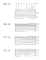
- FIGS. 1(a) to 1(d) are cross-sectional views illustrating the step of forming an impurity doped layer by ion implantation in a method for fabricating a semiconductor device according to a first embodiment of the present invention
- a method for fabricating a semiconductor device according to a first embodiment of the present invention is characterized in that a carbon layer is formed on a substrate surface by performing annealing in a reduced pressure atmosphere before an activation annealing process after ion implantation and then the activation annealing is performed continuously by raising a pressure and a temperature.
- FIG. 10 is a cross-sectional view showing the structure of an annealing furnace used in the method for fabricating the semiconductor device according to the present invention.
- the annealing furnace comprises: a reaction furnace 150; a susceptor 152 made of carbon which is for fixing a substrate 151; a support shaft 153; a coil 154 for heating a sample; a gas supply system 158 for supplying an argon gas 155, a hydrogen gas 156; and an oxygen gas 157 to the reaction furnace 150; a gas exhaust system 159 for exhausting the gasses in the reaction furnace 150 therefrom; piping 160 for exhaust gases; and a pressure adjustment valve 161.
- the susceptor 152 is covered with a heat insulating material 162 from therearound.
- the susceptor 152 supported by the support shaft 153 is heated by RF induction heating using the coil 154 wound around the reaction furnace 150.
- FIGS. 1(a) to 1(d) are cross-sectional views illustrating the method for fabricating the semiconductor device according to the first embodiment.
- a silicon carbide substrate 1 at an off-angle of 8 degrees in the [11-20] (112-bar 0) direction and with a diameter of 50 mm is prepared.
- an n-type 4H-SiC substrate e.g., is used.
- a silicon carbide thin film (silicon carbide film) 2 with a thickness of 10 ⁇ m is epitaxially grown by CVD on the silicon carbide substrate 1.
- impurity ions 3 are implanted into the silicon carbide thin film 2 by using an ion implantation apparatus, whereby an impurity ion implanted layer 4 is formed (see FIG. 1(b)).
- the impurity ions 3 to be implanted herein aluminum ions for forming, e.g., a p-type doped layer are selected. Specifically, the aluminum ions are implanted in multiple stages at seven acceleration voltages. At this time, the ions are individually implanted at a dose of 3 x 10 14 cm -3 by adjusting the acceleration voltage to 1.0 MeV, 1.6 MeV, and 2.4 MeV, at a dose of 7 x 10 14 cm -3 by adjusting the acceleration voltage to 3.3 MeV and 4.4 MeV, and at a dose of 3 x 10 14 cm -3 by adjusting the acceleration voltage to 5.6 MeV and 7.0 MeV. The substrate temperature during the ion implantation is adjusted to a room temperature. As a result, the impurity ion implanted layer 4 at a mean dopant concentration of about 5 x 10 18 cm -3 and with a thickness of 4 ⁇ m is formed.
- the silicon carbide substrate 1 formed with the impurity ion implanted layer 4 is placed on a susceptor 152 in the annealing furnace and then a chamber is internally evacuated by using the gas exhaust system 159.
- the degree of vacuum atmospheric pressure in the chamber
- an RF power of 20.0 kHz and 20 kW is applied to the coil for induction heating, thereby heating the silicon carbide substrate 1 to 1250 °C.
- annealing is performed for 60 minutes.
- a hydrogen gas may also be supplied, while maintaining a low pressure in the furnace. In this case, the presence of hydrogen allows easy debonding between silicon and carbon and facilitates selective sublimation of silicon.
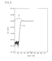
- FIG. 2 is a view showing the result of analyzing the substrate after activation annealing by using a secondary ion mass spectroscope (SIMS).
- SIMS secondary ion mass spectroscope
- a gas for annealing atmosphere (annealing gas) is supplied from the gas supply system 158, while the silicon carbide substrate 1 having the carbon layer 5 formed on the surface thereof remains heated at 1250 °C.
- annealing gas an argon gas 155 is selected and the flow rate of the gas is adjusted to 0.5 liters/minute.
- the pressure in the chamber is increased by using the pressure adjustment valve 161 to be held constant at 91 kPa.
- the substrate temperature is raised to 1750 °C and activation annealing is performed for 30 minutes, while the temperature is maintained.
- heating is terminated by halting the application of the RF power to the coil 154, while the argon gas 155 is supplied continuously, so that the substrate 151 is cooled.
- the aluminum ions in the impurity ion implanted layer 4 are activated so that the impurity doped layer 6 is formed in the silicon carbide thin film 2.
- the substrate temperature in the chamber of the annealing furnace is held constant at 800 °C for the removal of the carbon layer 5 and oxygen at a flow rate of 5 liters/minute is supplied so that a heating process is performed for 30 minutes.
- the carbon layer 5 as a substrate surface layer is completely removed and the impurity doped layer 6 is exposed.
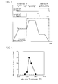
- FIG. 3 is a timing chart showing a substrate temperature, a pressure in the heating furnace, and an amount of gas supply which vary with time in the steps illustrated in FIGS. 1(b) to 1(d).
- the pressure in the heating furnace is held at a value at least under an atmospheric pressure, preferably at a value not lower than 10 -5 Pa and not higher than 10 Pa and the substrate temperature is adjusted to a level not lower than 1100 °C and not higher than 1400 °C, which is lower than the activation annealing temperature.
- FIG. 4 is a graph showing the relationship between the thickness of the carbon layer formed in FIG. 1(b) and the substrate temperature. From FIG. 4, it will be understood that the carbon layer has been formed when the substrate temperature is not lower than 1100 °C and not higher than 1400 °C.
- Si silicon
- C carbon
- Si is selectively sublimated from the impurity ion implanted layer 4 by thus limiting the temperature range so that only C remains in the substrate surface to consequently form the carbon layer 5.
- the adjustment of the pressure in the furnace to a value lower than the atmospheric pressure is for promoting the sublimation of Si.
- the process is performed preferably within the foregoing pressure range.
- the formation of the carbon layer 5 is possible provided that the substrate temperature is set in the above-mentioned range.
- the pressure in the heating furnace is maintained at a level at least higher than in the step of forming the carbon layer 5, preferably at a level not lower than 1 kPa and not higher than 100 kPa, by supplying an argon gas and the substrate temperature is adjusted to be not lower than 1500 °C and not higher than 2000 °C. Since the activation ratio of the impurity is generally proportional to the substrate temperature, the activation ratio in the impurity doped layer 6 can be adjusted to 80% or higher by increasing the substrate temperature to a level higher than in the step of forming the carbon layer 5 within the range in which the speed of sublimation of silicon carbide is not high.
- the "activation ratio" used herein indicates a value obtained by dividing the concentration of carriers contained in the impurity doped layer by the concentration (density) of the implanted impurity.
- the concentration of carriers can be calculated from an amount of current per unit area.
- the concentration (density) of the implanted impurity can be measured by SIMS or the like.
- an oxygen gas is supplied in the step shown in FIG. 1(d) in the state in which the substrate temperature has been adjusted to be not lower than 500 °C and not higher than 1000 °C.
- the carbon layer 5 can be removed by effectively causing a reaction between oxygen and the carbon layer 5 provided that the substrate temperature is not lower than 500 °C and not higher than 1000 °C.
- the most preferred substrate temperature is 800 °C since it allows the carbon layer 5 to be removed without causing the oxidation reaction of silicon carbide.
- the carbon layer can also be removed if a gas containing oxygen molecules is supplied instead of the oxygen gas.
- the present inventors analyzed the surface morphology of the substrate to which the activation annealing had been performed in accordance with the method described above by using an atomic force microscope (AFM).
- AFM atomic force microscope
- another silicon carbide substrate was prepared by implanting impurity ions thereinto under the same conditions as in the method according to the present embodiment and performing the prior-art activation annealing in an argon gas atmosphere with respect thereto.
- the conditions for the prior-art activation annealing were such that the substrate temperature was 1750 °C, the flow rate of an argon gas was 0.5 liters/minute, the pressure in the furnace during the annealing was held constant at 91 kPa, and the annealing time was 30 minutes.
- Measurement for the surface morphology of the substrate to which the activation annealing had been performed in accordance with the conventional method was also conducted by using the AFM.
- the activation annealing in accordance with the method of the present embodiment had achieved a two-order-of-magnitude reduction in the surface roughness of the substrate compared with the conventional method.
- the surface roughness of the upper surface of the substrate processed in accordance with the method of the present embodiment was about 0.5 nm.
- the "surface roughness" mentioned herein has the same meaning as the step height.
- the method of the present embodiment can also prevent the degradation of the characteristics of the semiconductor device by an impurity material contained in a resist or the like because the impurity is not brought into the heating furnace for performing the activation annealing.
- the formation of the carbon layer 5 for suppressing the occurrence of the macro-steps can be performed in the same heating furnace in which the activation annealing is performed, it is unnecessary to introduce a new apparatus and the steps for fabricating the semiconductor device can be simplified.
- the number of fabrication apparatus can be reduced and the fabrication steps can significantly be simplified compared with the case where the activation annealing and the removal of the carbon layer 5 are performed in different apparatus.
- the method described in the present embodiment has continuously performed the annealing for forming the carbon layer and the activation annealing for the implanted ions in the same furnace, the same effects as achieved by the method of the present embodiment are also achievable if the individual steps are performed in different heating furnaces.
- the method described in the present embodiment has continuously performed the activation annealing for the implanted ions and the removal of the carbon layer in the same furnace, the same effects as achieved by the method of the present embodiment are also achievable if the individual steps are performed in different heating furnaces.
- a silicon carbide substrate made of a polytype other than 4H-SiC may also be used instead.
- the carbon layer can also be formed even when n-type ions are implanted in accordance with the same method as described in the example.
- the silicon carbide semiconductor device fabricated in accordance with the method described above comprises: the silicon carbide substrate 1; the silicon carbide thin film 2 with a thickness of 10 ⁇ m provided on the principal surface of the silicon carbide substrate 1; and the impurity doped layer 6 with a thickness of 4 ⁇ m provided in the silicon carbide thin film 2.
- the impurity doped layer 6 a p-type impurity (aluminum or the like) at a concentration of, e.g., about 5 x 10 18 cm -3 has been contained.
- the silicon carbide semiconductor device has electrodes and the like provided on, e.g., the impurity doped layer 6 and on the back surface of the silicon carbide substrate 1, though they are not depicted herein, and operates as a semiconductor device such as a transistor or a diode.
- steps have been formed in the upper surface of the impurity doped layer 6 and the step height thereof is about not less than 0.1 nm and not more than 1 nm.
- the gate insulating film can be formed to have a uniform thickness and the movement of carriers is not disturbed by macro-steps. This makes it becomes possible to increase the breakdown voltage and allow a current at a high density to flow, which will be described later. Since the activation ratio of the p-type impurity in the impurity doped layer 6 has become 80% or higher, the intrinsic characteristics of the semiconductor device can be improved compared with the case where the activation ratio is low.
- FIGS. 5(a) to 5(c) and FIGS. 6(a) to 6(c) are cross-sectional views illustrating the method for fabricating the silicon carbide MOSFET according to the present embodiment.
- a silicon carbide substrate 21 is prepared.
- the silicon carbide substrate 21 there is used, e.g., a 4H-SiC substrate 1 having a principal surface thereof tilted at an off-angle of 8 degrees in the [11-20] (112-bar 0) direction from the (0001) plane and with a diameter of 50 mm.
- the substrate is of an n-type and the concentration of carriers therein is 1 x 10 18 cm -3 .
- an n-type impurity doped layer is grown epitaxially on the silicon carbide substrate 21 by CVD, whereby an n-type drift layer 22 with a thickness of 10 ⁇ m and at a carrier concentration of about 5 x 10 15 cm -3 is formed on the silicon carbide substrate 21 of the MOSFET.
- a first implant mask (not shown) composed of, e.g., a silicon dioxide film (SiO 2 ) is formed on the upper surface of the n-type drift layer 22 to form a first impurity implanted layer 23.
- the first implant mask covers a portion of the n-type drift layer 22 such that a region which will serve as the first ion implanted layer 23 later is opened.
- Al ions are implanted into the n-type drift layer 22 from above the first implant mask.
- the conditions for the implantation of the Al ions are assumed to be the same as in the method according to the first embodiment.
- the first implant mask is removed and then a second implant mask (not shown) made of SiO 2 is formed on the substrate such that a portion thereof is opened. Then, nitrogen ions are implanted into the first impurity ion implanted layer 23 through the opening of the second implant mask so that a second impurity ion implanted layer 24 is formed in the first impurity ion implanted layer 23.
- the substrate (the silicon carbide substrate 21 provided with the individual layers) is placed on the susceptor 152 in the annealing furnace and heated to 1250 °C in the state in which the chamber has been internally evacuated by using the gas exhaust system. In this state, annealing is performed for 180 minutes to form the carbon layer 25 with a thickness of about 100 nm.
- an argon gas is supplied at a flow rate of 0.5 liters/minute, while the temperature of the substrate is held constant at 1250 °C, to adjust the pressure in the chamber to 91 kPa. Thereafter, the substrate temperature is raised to 1750 °C and the activation annealing is performed for 30 minutes, while the temperature is maintained.
- the impurities contained in the first and second impurity ion implanted layers 23 and 24 are activated so that a p-type well region 26 and an n-type contact region for source 27 are formed.
- the activation ratio of the impurity in each of the p-type well region 26 and the n-type contact region for source 27 becomes 80% or more.
- a heating process for removing the carbon layer 25 is performed for 30 minutes by holding the substrate temperature in the chamber of the annealing furnace constant at 800 °C and supplying oxygen at a flow rate of 5 liters/minute.
- the process completely removes the carbon layer 25 provided over the silicon carbide substrate 21 and thereby exposes the p-type well region 26 and the contact region for source 27.
- the concentration of carriers contained in the p-type well region 26 is 1 x 10 17 cm -3 and the n-type contact region for source 27 containing carriers at a concentration of 1 x 10 18 cm -3 is formed.
- the height of each of steps formed in the respective upper surfaces of the p-type well region 26 and the contact region for source 27 after the activation annealing in this step is not less than 0.1 nm and not more than 1 nm so that the step height has been reduced to 1/10 or less of that in the case of using the conventional method.
- a gate insulating film 28 with a thickness of 30 nm is formed on the substrate surface by thermally oxidizing the substrate at 1100 °C.
- Ni is deposited on the upper surface of the contact region for source 27 and on the back surface of the silicon carbide substrate 21 by using an electron beam (EB) vapor deposition apparatus.
- heating at 1000 °C is performed by using a heating furnace, thereby forming a source electrode 29 serving as a first ohmic electrode on the contact region for source 27 and forming a drain electrode 30 serving as a second ohmic electrode on the back surface of the silicon carbide substrate 21.
- a gate electrode 31 is formed by vapor depositing aluminum on the gate insulating film 28, whereby the MOSFET having a structure as shown in FIG. 6(c) is formed.
- the MOSFET produced as described above comprises: the n-type silicon carbide substrate 21; the n-type drift layer 22 formed on the principal surface of the silicon carbide substrate 21; the p-type well region 26 provided in the n-type drift layer 22; the n-type contact region for source 27 provided in the p-type well region 26; the gate insulating film 28 provided over the n-type drift layer 22 and the p-type well region 26; the gate electrode 31 provided on the gate insulating film 28; the source electrode (ohmic electrode) 29 provided on the contact region for source 27; and the drain electrode 30 provided on the back surface of the silicon carbide substrate 21.
- the step height of steps formed in the respective upper surfaces of the p-type well region 26 and the contact region for source 27 is not less than 0.1 nm and not more than 1 nm.
- the step height of the steps formed in the upper surface of the n-type drift layer 22 is substantially uniform in each of the ion implanted region thereof and in the region thereof without ion implantation.
- a MOSFET produced by performing activation annealing using the prior-art technology was prepared.
- the conditions for the prior-art activation annealing were such that the substrate temperature was 1750 °C, the flow rate of the argon gas was 0.5 liters/minute, the pressure in the furnace during the annealing was held constant at 91 kPa, and the annealing time was 30 minutes.
- the MOSFET produced by using the prior art technology was designed to have the same device structure as the MOSFET according to the present embodiment.
- the drain current in the MOSFET according to the present embodiment was triple or more the drain current in the MOSFET formed by using the prior art technology.
- a conceivable reason for this is that, since the step height (surface roughness) is 10 nm or more in the conventional MOSFET, the mobility of carriers flowing in the vicinity of the surface of the p-type well region 26 has lowered and the drain current has become less likely to flow.
- the step height in each of the p-type well region 26 and the contact region for source 27 is 1 nm or less in the MOSFET according to the present embodiment, it may be considered that the mobility of carriers has not lowered and the drain current at a high current density is allowed to flow.
- a MESFET in which a gate electrode forming a Schottky barrier with a silicon carbide thin film and source and drain electrodes each in ohmic contact with the silicon carbide thin film are further provided, a Schottky diode comprising a Schottky electrode provided on a silicon carbide thin film and an ohmic electrode provided on the back surface of the silicon carbide substrate, or the like.
- the electric characteristics of even a silicon carbide semiconductor device other than the MOSFET fabricated by using an ion implantation technology can be improved by rendering the upper surface of the impurity doped layer more flat than in the conventional embodiment.
- a Schottky diode Besides the MOSFET described in the second embodiment, a Schottky diode, a MESFET, and the like are also fabricated by using an ion implantation technology so that the fabrication method according to the present invention is applicable thereto. A description will be given herein below to a method for reducing the size of each of macro-steps in these devices.
- FIGS. 7(a) to 7(d) are cross-sectional views illustrating a method for fabricating a Schottky diode according to an embodiment of the present invention.
- an n-type epitaxially grown layer 32 with a thickness of 10 ⁇ m and at a carrier concentration of about 5 x 10 15 cm -3 is formed by CVD on an n-type silicon carbide substrate 31.
- the concentration of carriers contained herein in the n-type silicon carbide substrate 31 is 1 x 10 18 cm -3 .
- Al ions are implanted in parts of the epitaxially grown layer 32 to form guard rings 33a.
- the substrate temperature is adjusted to 1250 °C and held constant for 180 minutes, whereby a carbon layer 35 with a thickness of 100 nm is formed on the substrate.
- the impurity in each of the guard rings 33a is activated by raising the substrate temperature to 1750 °C by using the same heating furnace as used in the annealing step so that guard rings 33 are formed.
- nickel is vapor deposited on the back surface of the n-type silicon carbide substrate 31 and heated at 1000 °C to form an ohmic electrode 39.
- Ti titanium is vapor deposited on the upper surface of the epitaxially grown layer 32 to form a Schottky electrode 37.
- the Schottky diode thus fabricated comprises: the n-type silicon carbide substrate 31; the epitaxially grown layer 32 made of n-type SiC provided on the n-type silicon carbide substrate 31; the Schottky electrode made of Ti provided on the epitaxially grown layer 32; the guard rings 33 provided in the regions of the epitaxially grown layer 32 which are located under and on both sides of the Schottky electrode 37 and containing the p-type impurity; and the ohmic electrode 39 made of Ni provided on the back surface of the n-type silicon carbide substrate 31, as shown in FIG. 7(d).
- the step height at the upper surface of the epitaxially grown layer 32 of the Schottky diode according to the present embodiment has been reduced to a level not lower than 0.1 nm and not higher than 1 nm.
- the localization of an electric field at the interface between the Schottky electrode 37 and the epitaxially grown layer 32 can be suppressed more effectively than in a conventional Schottky diode and the breakdown voltage can be increased.
- FIGS. 8(a) to 8(d) are cross-sectional views illustrating a method for fabricating an MESFET according to an embodiment of the present invention.
- an undoped layer 43 made of silicon carbide with a thickness of 10 ⁇ m is grown by CVD on a silicon carbide substrate 41. Then, a channel layer 45 made of silicon carbide with a thickness of 200 nm and at a carrier concentration of about 5 x 10 17 cm -3 is grown on the undoped layer 43.
- nitrogen ions are implanted in parts of each of the channel layer 45 and the undoped layer 43 to form a contact region for source 47a and a contact region for drain 49a such that the portion (the channel layer 45 shown in FIG. 8(c) and the subsequent drawings) of the channel layer 45 which is undoped with the impurity is sandwiched therebetween.
- an annealing process at 1250 °C is performed with respect to the substrate for 180 minutes to form a carbon layer 51 with a thickness of 100 nm on the substrate.
- activation annealing is performed by raising the substrate temperature to 1750 °C by using the same heating furnace as used in the annealing step to form a source region 47 and a drain region 49.
- Ni is deposited on the upper surface of each of the source region 47 and the drain region 49 and heated at 1000 °C, thereby forming a source electrode 53 and a drain electrode 55. Further, Ti is vapor deposited on the upper surface of the channel layer 45 to form a gate electrode.
- the MESFET thus fabricated according to the present embodiment comprises: the silicon carbide substrate 41; the undoped layer 43 made of undoped SiC with a thickness of 10 ⁇ m provided on the silicon carbide substrate 41; the channel layer 45 made of SiC containing the n-type impurity provided on the undoped layer 43; the gate electrode 57 provided on the channel layer 45; the source and drain regions 47 and 49 formed in the regions of the undoped layer 43 and the channel layer 45 which are located under and on both sides of the gate electrode 57; the source electrode 53 provided on the source region 47; and the drain electrode provided on the drain region 49.
- the step height at the upper surface of each of the source region 47, the drain region 49, and the channel layer 45 has been reduced to a level not lower than 0.1 nm and not higher than 1 nm. Consequently, in the MESFET according to the present embodiment, the disturbance of carriers has been suppressed more effectively than in a conventional MESFET and transconductance has been improved.
- a silicon carbide semiconductor device according to the present invention is used preferably in a device required to operate at a high voltage, such as a plasma display.
Landscapes
- Electrodes Of Semiconductors (AREA)
- Insulated Gate Type Field-Effect Transistor (AREA)
- Carbon And Carbon Compounds (AREA)
- Bipolar Transistors (AREA)
- Junction Field-Effect Transistors (AREA)
- Crystals, And After-Treatments Of Crystals (AREA)
Abstract
Description
- The present invention relates to a semiconductor device using a silicon carbide substrate and to a method for fabricating the same.
- Silicon carbide (SiC) is a semiconductor material the application of which to a next-generation low-loss power device or the like is expected because it features a larger band gap than silicon (Si) and a higher field intensity at which a dielectric breakdown occurs. Silicon carbide has numerous polytypes including cubic-type 3C-SiC and hexagonal-type 6H-SiC and 4H-SiC. Of these polytypes, 6H-SiC and 4H-SiC are used commonly to produce practically usable silicon carbide semiconductor devices. Among them, a silicon carbide substrate (SiC substrate) having a principal surface which is substantially coincident with the (0001) plane perpendicular to the crystal axis of the c-axis is used mostly for a silicon carbide semiconductor device (SiC semiconductor device).
- To form a silicon carbide semiconductor device, it is necessary to form an epitaxially grown layer serving as the active region of the semiconductor device on a silicon carbide substrate and control the conductivity type and carrier concentration of a selected region in the epitaxially grown layer. To form an impurity doped layer in the selected local region, a technology which ion-implants an impurity dopant into the epitaxially grown layer is used.
- A description will be given herein below to a typical method for forming a MOSFET made of silicon carbide by using the ion implantation technology.
- FIGS. 9(a) to 9(d) are cross-sectional views illustrating the typical method for forming the MOSFET made of silicon carbide.
- First, in the step shown in FIG. 9(a), a silicon carbide thin film is epitaxially grown on a
silicon carbide substrate 140 to form an n-type drift layer 141. In this step, the density of steps in the surface of the substrate is increased by intentionally imparting a slight angle (at several degrees) to the (0001) plane of thesilicon carbide substrate 140 so that the silicon carbide thin film is grown by a step flow process which involves the lateral growth of the steps. At present, it is common practice to impart an off-angle of 8° to 4H-SiC and an off angle of 3.5° to 6H-SiC, each in the [11-20] direction by using the (0001) plane as a reference plane. - Subsequently, in the step shown in FIG. 9(b), an
implant mask 142 for ion implantation is formed on the upper surface of the n-type drift layer 141. Theimplant mask 142 covers a portion of the n-type drift layer 141 such that a region, which will serve as a p-type well region 143 in the subsequent step, is opened. - Next, in the step shown in FIG. 9(c),
Al ions 144 are implanted into the n-type drift layer 141 from above theimplant mask 142. - Then, in the step shown in FIG. 9(d), the
implant mask 142 is removed. Thereafter, an activation annealing process is performed by heating thesilicon carbide substrate 140 in an inert gas (e.g., argon gas) atmosphere to a temperature not lower than 1700 °C to recover the damage caused by the ion implantation and activate the implanted impurity ions. By the activation annealing process, a p-type well region 143 is formed in a part of the n-type drift layer 141. - By subsequently performing additional ion implantation and the formation of electrodes, a vertical MOSFET can be fabricated.
- However, since the silicon carbide substrate is processed at a high temperature in the step shown in FIG. 9(d),
macro-steps 145 are formed disadvantageously in the upper surface of the region into which the ions have been implanted. In addition,macro-steps 146 are also formed in the upper surface of the region into which ions have not been implanted, though themacro-steps 146 are smaller in size than themacro-steps 145 in the ion implanted region. A macro-step is a bunch of combined steps each formed at a depth corresponding to several atomic layers in the surface of a silicon carbide thin film. In a prior art technology as shown in FIGS. 9, projections and depressions formed due to the macro-steps in the upper surface of the silicon carbide thin film after the activation annealing have presented a great obstacle to an improvement in the performance of the semiconductor device. A conceivable reason for themacro-steps 145 formed in the ion implanted region which are larger in size than themacro-steps 146 formed in the region without ion implantation is that the damage caused by the ion implantation has rendered silicon atoms and carbon atoms more likely to be desorbed from the surface of the silicon carbide thin film. The size of each of themacro-steps 145 is larger as the temperature for the activation annealing is higher. There are cases where a step height (see FIG. 9(d)) reaches several tens of nanometers and the width of a terrace reaches several hundreds of nanometers. - The formation of the macro-steps has caused performance degradation in numerous semiconductor devices including a MOSFET. In the case with, e.g., a Schottky diode, the problem is encountered that the localization of an electric field to the tip portions of macro-steps occurs in a Schottky electrode formed on the upper surface of a silicon carbide thin film and the breakdown voltage thereof is thereby lowered. In the case with a MESFET in which a current flows in the surface layer of a silicon carbide thin film, the problem is encountered that the disturbance of carriers occurs in macro-steps to lower mobility and reduce transconductance. A MOSFET in which a gate oxide film is formed by thermal oxidation on the upper surface of a silicon carbide thin film encounters the problem that the formation of an oxide film having different thicknesses at the sidewall and terrace portions of macro-steps causes the non-uniform thickness of an inversion layer formed by applying a gate voltage and the lowering of channel mobility. Thus, in accordance with the conventional method, even when a semiconductor device is produced by using silicon carbide, it has been difficult to obtain electric characteristics expected from the inherently excellent physical property values of silicon carbide.
- To prevent the steps from being formed in the upper surface of a silicon carbide thin film by activation annealing, it has been proposed to form a diamond-like carbon (DLC) film or a photoresist as a protective film on the upper surface of the silicon carbide thin film prior to the activation annealing (see, e.g., Patent Document 1).
- Patent Document 1:
Japanese Laid-Open Patent Publication No. 2001-68428 - However, a conventional silicon carbide semiconductor device and a method for fabricating the same as disclosed in
Patent Document 1 has had the following problems. - Since the diamond-like carbon film or the photoresist is formed as the protective -film on the upper surface of the silicon carbide thin film, the problem is encountered that the number of the fabrication steps for a semiconductor device is increased disadvantageously. Depending on the structure of the semiconductor device, it is necessary to perform a plurality of steps of activation annealing and the conventional method has necessitated the formation of the protective film in each step of activation annealing. In addition, a new apparatus is required to form such a protective film, which increases fabrication cost. Moreover, the problem is also encountered that the step of removing the protective film after the activation annealing and an apparatus for removing the protective film become necessary.
- In addition to these problems, there is also the possibility that, when the activation annealing is performed at a high temperature not lower than 1600 °C, an impurity material in the protective film may be diffused into the silicon carbide thin film or the impurity material sublimated from the protective film contaminates the inside of an annealing furnace. When contamination by such an impurity occurs, the characteristics of a silicon carbide semiconductor device are degraded significantly.
- Thus, even though the formation of step bunching can be suppressed by such countermeasures, it has been extremely difficult to form a silicon carbide semiconductor device having excellent characteristics. Accordingly, there have been demands for a silicon carbide semiconductor device in which projections and depressions are not formed in the surface by activation annealing and the characteristics are not degraded by an impurity material and a fabrication method therefor.
- In view of the foregoing problems, an object of the present invention is to provide a method for fabricating a silicon carbide semiconductor device which allows the upper surface of a silicon carbide thin film to retain flatness, while increasing the activation ratio of the implanted impurity, and a silicon carbide semiconductor device fabricated by the method.
- To solve the foregoing problems, a method for fabricating a silicon carbide semiconductor device according to the present invention comprises the steps of: (a) implanting impurity ions into a silicon carbide layer (including a silicon carbide substrate and a silicon carbide film grown epitaxially on a silicon carbide substrate); (b) heating the silicon carbide layer to form a carbon layer on a surface of the silicon carbide layer; and (c) after the step (b), performing an activation annealing process with respect to the silicon carbide layer in an atmosphere at a temperature higher than in the step (b).
- Since the method allows the activation annealing process in the step (c) to be performed in the state in which the carbon layer has been formed, macro-steps formed in the surface of the ion implanted region can be reduced in size even when the activation annealing is performed at a high temperature. As a result, it becomes possible to produce a semiconductor device in which the upper surface of the silicon carbide substrate or the silicon carbide film is more flat than in the conventional embodiment without lowering the activation ratio of the impurity implanted in the silicon carbide substrate or the silicon carbide film. By the method according to the present invention, the contamination of the semiconductor device with an impurity material such as the component of a resist film can particularly be prevented because the carbon layer serving as a protective film is generated from the silicon carbide substrate or the silicon carbide film.
- The step (b) includes forming the carbon layer under a pressure condition lower than an atmospheric pressure and the step (c) includes performing the activation annealing process under a pressure condition higher than in the step (b). The arrangement promotes the sublimation of silicon from the surface of the silicon carbide substrate or the silicon carbide film in the step (b) and thereby allows the carbon layer to be formed more promptly than in the case where the step (b) is performed under the same pressure condition as in the step (c).
- Preferably, the steps (b) and (c) are performed in the same heating furnace. The arrangement allows a reduction in the types of the apparatus to be used and the simplification of the process steps.
- The step (b) includes forming the carbon layer in the presence of a gas containing hydrogen. The arrangement is preferred since it promotes the formation of the carbon layer.
- Preferably, the step (b) includes forming the carbon layer under a pressure condition not lower than 1x 10⁻⁵ Pa and not higher than 10 Pa. This is because, when the pressure is higher than 10 Pa, steps are formed disadvantageously by the heating process in the upper surface of the silicon carbide substrate or the silicon carbide film and, when the pressure is lower than 10-5 Pa, even carbon may be sublimated undesirably by the heating process.
- Preferably, a temperature of the silicon carbide layer is not lower than 1100 °C and not higher than 1400 °C in the step (b). This is because, when the substrate temperature is lower than 1100 °C, the sublimation of silicon from the substrate surface does not occur and, when the substrate temperature is higher than 1400 °C, even carbon may be sublimated undesirably.
- Preferably, the step (c) includes performing the activation annealing process by adjusting a temperature of the silicon carbide layer to a range not lower than 1500 °C and not higher than 2000 °C under a pressure condition not lower than 1 kPa and not higher than 100 kPa. This is because, by performing the activation annealing in this pressure range and this temperature range, the activation ratio of the impurity can be increased sufficiently.
- The method further comprises the step of: (d) after the step (c), heating the silicon carbide layer in the presence of a gas containing oxygen atoms to remove the carbon layer. The arrangement causes the carbon film to react with oxygen molecules and thereby allows the removal of the carbon film.
- If a temperature of the silicon carbide layer is not lower than 500 °C and not higher than 1000 °C in the step (d), the carbon layer can be removed more reliably. In particular, the substrate temperature is adjusted preferably to 800 °C. The arrangement allows more efficient removal of the carbon layer without causing the oxidation reaction of silicon carbide.
- The removal of the carbon layer in the step (d) is performed in the same heating furnace as the activation annealing process in the step (c). The arrangement allows a reduction in the types of the apparatus to be used and the simplification of the process steps.
- A silicon carbide semiconductor device according to the present embodiment comprises: a silicon carbide layer; an impurity doped layer formed in a part of the silicon carbide layer; and an electrode provided on the silicon carbide layer, wherein a step height at an upper surface of the silicon carbide layer is substantially the same in the impurity doped layer and in a region of the silicon carbide layer other than the impurity doped layer. In the present specification and the scope of claims, a "step height" indicates a value obtained by dividing the sum of the heights of all steps in a 10-µm square region on the surface of the silicon carbide layer by the number of the steps, while the "height of a step" indicates the height difference between the crystal planes of two adjacent steps (the height difference in a direction perpendicular to the crystal planes), as shown in FIG. 9(d). An impurity doped layer. according to the present invention is exposed at a part of the upper surface of a silicon carbide layer.
- The achievement of substantially the same step height in the impurity doped layer of the silicon carbide layer and the region thereof other than the impurity doped layer is enabled by the method for fabricating a silicon carbide semiconductor device according to the present invention. That is, by generating the carbon layer from the silicon carbide layer such that it is located on the upper surface thereof, bonds are strong at the interface between the carbon layer and the silicon carbide layer so that, even when annealing for activating the impurity is performed, the formation of macro-steps in the upper surface of the silicon carbide layer is suppressed. In contrast to a conventional embodiment in which macro-steps are formed in an impurity doped layer to be larger than in the other region, the present invention allows the impurity doped layer and the other region to be protected by the carbon layer which is coupled with strong bonds to the silicon carbide layer so that the step height is substantially the same in either of the regions.
- In the silicon carbide semiconductor device according to the present invention, the mobility of carriers can be improved in the case where, e.g., a current flows in the vicinity of the upper surface of the impurity doped layer. Otherwise, it is also possible to reduce the localization of an electric field and increase the breakdown voltage in the case where a Schottky electrode is provided on the impurity doped layer.
- Preferably, the step height at the upper surface of the silicon carbide layer is not less than 0.1 nm and not more than 1 nm. In this case, in particular, a silicon carbide semiconductor device can be implemented which features a high breakdown voltage and allows a current to flow with high-density.
- To form the carbon layer from the silicon carbide layer in the step of forming the silicon carbide semiconductor device according to the present invention, a concentration of an element in the impurity doped layer other than carbon, silicon, and a dopant of the impurity doped layer is held at a value not higher than 1 x 1014 cm-3. In the conventional embodiment, when a diamond-like carbon film or a photoresist is used as the protective film, there is the possibility that the impurity contained in the protective film may be diffused into a silicon carbide layer to degrade the characteristics of the silicon carbide semiconductor device. By contrast, the present invention uses carbon originally contained in the silicon carbide layer so that the characteristics of the silicon carbide semiconductor device are prevented from degradation.
- Although diamond-like carbon is made of carbon, there is the possibility that an impurity such as chromium, nickel, iron, or manganese in a SUS chamber may be mixed in diamond-like carbon during the formation thereof by plasma CVD. When diamond-like carbon is used for the protective film, the impurity may enter the silicon carbide layer.
- On the other hand, a resist is made of carbon, hydrogen, and oxygen. When the resist is used as the protective film, there is the possibility that these elements may be diffused into the silicon carbide layer.
- From the foregoing, it will be understood that the concentrations of impurities contained in diamond-like carbon or a resist are lower in the silicon carbide semiconductor device according to the present invention than in the conventional embodiment. Specifically, the concentrations of hydrogen, oxygen, chromium, nickel, manganese, and iron are lower.
- The silicon carbide semiconductor device according to the present invention may further comprise: a gate insulating film provided on the silicon carbide layer; a gate electrode provided on the gate insulating film; and a first electrode in ohmic contact with the silicon carbide layer. In this case, since the gate insulating film is allowed to have a more uniform thickness than in the conventional embodiment, the gate breakdown voltage can be increased.
- Alternatively, the silicon carbide semiconductor device according to the present invention may further comprise: a silicon carbide substrate provided on a lower surface of the silicon carbide layer; and a second electrode in ohmic contact with a lower surface of the silicon carbide substrate. In this case, the characteristics of a device in which a current flows vertically such as, e.g., a vertical MOSFET can be improved.
- Alternatively, the silicon carbide semiconductor device according to the present invention may further comprise: a third electrode in Schottky contact with the silicon carbide layer. In this case, since a Schottky barrier can be formed excellently between the silicon carbide film and the second electrode, the semiconductor device with an increased breakdown voltage can be implemented.
- Thus, the method for fabricating the semiconductor device according to the present invention allows a silicon carbide semiconductor device which realizes a high activation ratio to be provided, while allowing a silicon carbide semiconductor film to retain a flat surface.
- FIGS. 1(a) to 1(d) are cross-sectional views illustrating the step of forming an impurity doped layer by ion implantation in a method for fabricating a semiconductor device according to a first embodiment of the present invention;
- FIG. 2 is a view showing the result of analyzing a substrate after activation annealing by using a secondary ion mass spectroscope (SIMS);
- FIG. 3 is a timing chart showing a substrate temperature, a pressure in a heating furnace, and an amount of gas supply which vary with time in the step illustrated in FIGS. 1(b) to 1(d);
- FIG. 4 is a graph showing the relationship between the thickness of a carbon layer formed in FIG. 1(b) and the substrate temperature;
- FIGS. 5(a) to 5(c) are cross-sectional views illustrating a method for fabricating a silicon carbide MOSFET according to a second embodiment of the present invention;
- FIGS. 6(a) to 6(c) are cross-sectional views illustrating the method for fabricating the silicon carbide MOSFET according to the second embodiment;
- FIGS. 7(a) to 7(d) are cross-sectional views illustrating a method for fabricating a Schottky diode according to an embodiment of the present invention;
- FIGS. 8(a) to 8(d) are cross-sectional views illustrating a method for fabricating a MOSFET according to an embodiment of the present invention;
- FIGS. 9(a) to 9(d) are cross-sectional views illustrating a typical method for forming a MOSFET made of silicon carbide; and
- FIG. 10 is a cross-sectional view showing the structure of an annealing furnace used in the method for fabricating a semiconductor device according to the present invention.
-
- 1
- Silicon Carbide Substrate
- 2
- Silicon Carbide Thin Film
- 3
- Impurity Ions
- 4
- Impurity Ion Implanted Layer
- 5, 25
- Carbon Layer
- 6
- Impurity Doped Layer
- 21
- Silicon Carbide Substrate
- 22
- n-Type Drift Layer
- 23
- First Impurity Ion Implanted Layer
- 24
- Second Impurity Ion Implanted layer
- 26
- p-Type Well Region
- 27
- Contact Region for Source
- 28
- Gate Insulating Film
- 29
- Source Electrode
- 30
- Drain Electrode
- 31
- Gate Electrode
- 150
- Reaction Furnace
- 151
- Substrate
- 152
- Susceptor
- 153
- Support Shaft
- 154
- Coil
- 155
- Argon Gas
- 156
- Hydrogen Gas
- 157
- Oxygen Gas
- 158
- Gas Supply System
- 159
- Gas Exhaust System
- 160
- Piping for Exhaust Gas
- 161
- Pressure Adjustment Valve
- 162
- Heat Insulating Material
- (Embodiment 1)
A method for fabricating a semiconductor device according to a first embodiment of the present invention is characterized in that a carbon layer is formed on a substrate surface by performing annealing in a reduced pressure atmosphere before an activation annealing process after ion implantation and then the activation annealing is performed continuously by raising a pressure and a temperature. Referring to the drawings, the semiconductor device and the method for fabricating the same according to the first embodiment will be described herein below. - FIG. 10 is a cross-sectional view showing the structure of an annealing furnace used in the method for fabricating the semiconductor device according to the present invention. As shown in the drawing, the annealing furnace comprises: a
reaction furnace 150; asusceptor 152 made of carbon which is for fixing asubstrate 151; asupport shaft 153; acoil 154 for heating a sample; agas supply system 158 for supplying anargon gas 155, ahydrogen gas 156; and anoxygen gas 157 to thereaction furnace 150; agas exhaust system 159 for exhausting the gasses in thereaction furnace 150 therefrom; piping 160 for exhaust gases; and apressure adjustment valve 161. Thesusceptor 152 is covered with aheat insulating material 162 from therearound. Thesusceptor 152 supported by thesupport shaft 153 is heated by RF induction heating using thecoil 154 wound around thereaction furnace 150. - A description will be given to the method for fabricating the semiconductor device which forms a carbon layer on a silicon carbide substrate after ion implantation by using the annealing furnace and performs activation annealing thereafter.
- FIGS. 1(a) to 1(d) are cross-sectional views illustrating the method for fabricating the semiconductor device according to the first embodiment.
- First, in the step shown in FIG 1(a), a
silicon carbide substrate 1 at an off-angle of 8 degrees in the [11-20] (112-bar 0) direction and with a diameter of 50 mm is prepared. As thesilicon carbide substrate 1, an n-type 4H-SiC substrate, e.g., is used. Then, a silicon carbide thin film (silicon carbide film) 2 with a thickness of 10 µm is epitaxially grown by CVD on thesilicon carbide substrate 1. Subsequently,impurity ions 3 are implanted into the silicon carbidethin film 2 by using an ion implantation apparatus, whereby an impurity ion implanted layer 4 is formed (see FIG. 1(b)). As theimpurity ions 3 to be implanted herein, aluminum ions for forming, e.g., a p-type doped layer are selected. Specifically, the aluminum ions are implanted in multiple stages at seven acceleration voltages. At this time, the ions are individually implanted at a dose of 3 x 1014 cm-3 by adjusting the acceleration voltage to 1.0 MeV, 1.6 MeV, and 2.4 MeV, at a dose of 7 x 1014 cm-3 by adjusting the acceleration voltage to 3.3 MeV and 4.4 MeV, and at a dose of 3 x 1014 cm-3 by adjusting the acceleration voltage to 5.6 MeV and 7.0 MeV. The substrate temperature during the ion implantation is adjusted to a room temperature. As a result, the impurity ion implanted layer 4 at a mean dopant concentration of about 5 x 1018 cm-3 and with a thickness of 4 µm is formed. - Subsequently, in the step shown in FIG. 1(b), the
silicon carbide substrate 1 formed with the impurity ion implanted layer 4 is placed on asusceptor 152 in the annealing furnace and then a chamber is internally evacuated by using thegas exhaust system 159. At this time, the degree of vacuum (atmospheric pressure in the chamber) is adjusted to about 10-4 Pa. In the state in which the chamber has been internally evacuated, an RF power of 20.0 kHz and 20 kW is applied to the coil for induction heating, thereby heating thesilicon carbide substrate 1 to 1250 °C. In this state, annealing is performed for 60 minutes. At this time, a hydrogen gas may also be supplied, while maintaining a low pressure in the furnace. In this case, the presence of hydrogen allows easy debonding between silicon and carbon and facilitates selective sublimation of silicon. - FIG. 2 is a view showing the result of analyzing the substrate after activation annealing by using a secondary ion mass spectroscope (SIMS). As shown in the drawing, the result of the compositional analysis of the upper portion of the substrate shows that the carbon layer 5 with a thickness of about 30 nm has been formed on the substrate surface, i.e., on the impurity ion implanted layer 4.
- Next, in the step shown in FIG. 1(c), a gas for annealing atmosphere (annealing gas) is supplied from the
gas supply system 158, while thesilicon carbide substrate 1 having the carbon layer 5 formed on the surface thereof remains heated at 1250 °C. As the annealing gas, anargon gas 155 is selected and the flow rate of the gas is adjusted to 0.5 liters/minute. Then, the pressure in the chamber is increased by using thepressure adjustment valve 161 to be held constant at 91 kPa. Thereafter, the substrate temperature is raised to 1750 °C and activation annealing is performed for 30 minutes, while the temperature is maintained. Then, heating is terminated by halting the application of the RF power to thecoil 154, while theargon gas 155 is supplied continuously, so that thesubstrate 151 is cooled. By the activation annealing process, the aluminum ions in the impurity ion implanted layer 4 are activated so that the impurity dopedlayer 6 is formed in the silicon carbidethin film 2. - Subsequently, in the step shown in FIG. 1(d), the substrate temperature in the chamber of the annealing furnace is held constant at 800 °C for the removal of the carbon layer 5 and oxygen at a flow rate of 5 liters/minute is supplied so that a heating process is performed for 30 minutes. By this process, the carbon layer 5 as a substrate surface layer is completely removed and the impurity doped
layer 6 is exposed. - After this step, by passing through the steps including, e.g., the formation of an electrode on the impurity doped
layer 6, various semiconductor devices such as a MOSFET can be produced. - FIG. 3 is a timing chart showing a substrate temperature, a pressure in the heating furnace, and an amount of gas supply which vary with time in the steps illustrated in FIGS. 1(b) to 1(d).
- As shown in the drawing, in the step of forming the carbon layer 5 shown in FIG. 1(b), the pressure in the heating furnace is held at a value at least under an atmospheric pressure, preferably at a value not lower than 10-5 Pa and not higher than 10 Pa and the substrate temperature is adjusted to a level not lower than 1100 °C and not higher than 1400 °C, which is lower than the activation annealing temperature. FIG. 4 is a graph showing the relationship between the thickness of the carbon layer formed in FIG. 1(b) and the substrate temperature. From FIG. 4, it will be understood that the carbon layer has been formed when the substrate temperature is not lower than 1100 °C and not higher than 1400 °C. This is because the sublimation of silicon (Si) does not occur when the substrate temperature is lower than 1100 °C and even carbon (C) is sublimated undesirably when the substrate temperature is higher than 1400 °C. That is, since Si is sublimated at a temperature lower than C, Si is selectively sublimated from the impurity ion implanted layer 4 by thus limiting the temperature range so that only C remains in the substrate surface to consequently form the carbon layer 5. The adjustment of the pressure in the furnace to a value lower than the atmospheric pressure is for promoting the sublimation of Si. However, since even C is sublimated by the heating process when the pressure in the furnace becomes lower than 10-5 Pa and steps are formed disadvantageously in the substrate surface when the pressure in the furnace exceeds 10 Pa, the process is performed preferably within the foregoing pressure range. The formation of the carbon layer 5 is possible provided that the substrate temperature is set in the above-mentioned range.
- Subsequently, in the activation annealing step shown in FIG 1(c), the pressure in the heating furnace is maintained at a level at least higher than in the step of forming the carbon layer 5, preferably at a level not lower than 1 kPa and not higher than 100 kPa, by supplying an argon gas and the substrate temperature is adjusted to be not lower than 1500 °C and not higher than 2000 °C. Since the activation ratio of the impurity is generally proportional to the substrate temperature, the activation ratio in the impurity doped
layer 6 can be adjusted to 80% or higher by increasing the substrate temperature to a level higher than in the step of forming the carbon layer 5 within the range in which the speed of sublimation of silicon carbide is not high. In the present specification, the "activation ratio" used herein indicates a value obtained by dividing the concentration of carriers contained in the impurity doped layer by the concentration (density) of the implanted impurity. The concentration of carriers can be calculated from an amount of current per unit area. The concentration (density) of the implanted impurity can be measured by SIMS or the like. - Then, after the supply of the argon gas is halted, an oxygen gas is supplied in the step shown in FIG. 1(d) in the state in which the substrate temperature has been adjusted to be not lower than 500 °C and not higher than 1000 °C. In this step, the carbon layer 5 can be removed by effectively causing a reaction between oxygen and the carbon layer 5 provided that the substrate temperature is not lower than 500 °C and not higher than 1000 °C. However, the most preferred substrate temperature is 800 °C since it allows the carbon layer 5 to be removed without causing the oxidation reaction of silicon carbide. The carbon layer can also be removed if a gas containing oxygen molecules is supplied instead of the oxygen gas.
- Then, the present inventors analyzed the surface morphology of the substrate to which the activation annealing had been performed in accordance with the method described above by using an atomic force microscope (AFM). For the sake of comparison, another silicon carbide substrate was prepared by implanting impurity ions thereinto under the same conditions as in the method according to the present embodiment and performing the prior-art activation annealing in an argon gas atmosphere with respect thereto. The conditions for the prior-art activation annealing were such that the substrate temperature was 1750 °C, the flow rate of an argon gas was 0.5 liters/minute, the pressure in the furnace during the annealing was held constant at 91 kPa, and the annealing time was 30 minutes. Measurement for the surface morphology of the substrate to which the activation annealing had been performed in accordance with the conventional method was also conducted by using the AFM.
- As a result of making a comparison between the respective surface morphologies resulting from the activation annealing in accordance with the method of the present embodiment and from the prior-art activation annealing, it was proved that the activation annealing in accordance with the method of the present embodiment had achieved a two-order-of-magnitude reduction in the surface roughness of the substrate compared with the conventional method. The surface roughness of the upper surface of the substrate processed in accordance with the method of the present embodiment was about 0.5 nm. The "surface roughness" mentioned herein has the same meaning as the step height. As a result of examining the activation ratio of aluminum ions in the substrate processed in accordance with the method of the present embodiment, it was also proved that an extremely high activation ratio of about 90% was achieved.
- These results indicate that the method of the present embodiment allows a high activation ratio to be achieved, while retaining a flat surface. By contrast, it has been difficult to achieve both an improvement in activation ratio and the suppression of the occurrence of macro-steps by using the prior-art technology because, if the temperature for the activation annealing is increased, the activation ratio is increased but the macro-steps are also increased in size.
- In addition, the method of the present embodiment can also prevent the degradation of the characteristics of the semiconductor device by an impurity material contained in a resist or the like because the impurity is not brought into the heating furnace for performing the activation annealing. Moreover, since the formation of the carbon layer 5 for suppressing the occurrence of the macro-steps can be performed in the same heating furnace in which the activation annealing is performed, it is unnecessary to introduce a new apparatus and the steps for fabricating the semiconductor device can be simplified. Since it is also possible to perform the removal of the carbon layer 5 in the same heating furnace in which the activation annealing is performed, the number of fabrication apparatus can be reduced and the fabrication steps can significantly be simplified compared with the case where the activation annealing and the removal of the carbon layer 5 are performed in different apparatus.
- Although the method described in the present embodiment has continuously performed the annealing for forming the carbon layer and the activation annealing for the implanted ions in the same furnace, the same effects as achieved by the method of the present embodiment are also achievable if the individual steps are performed in different heating furnaces.
- Although the method described in the present embodiment has continuously performed the activation annealing for the implanted ions and the removal of the carbon layer in the same furnace, the same effects as achieved by the method of the present embodiment are also achievable if the individual steps are performed in different heating furnaces.
- Although the embodiment described above has removed the carbon layer by thermal oxidation, the same effects as achieved by the method of the present embodiment are also achievable if the carbon layer is removed by a plasma process or an ozone process using oxygen.
- Although the embodiment described above has used 4H-SiC for the silicon carbide substrate, a silicon carbide substrate made of a polytype other than 4H-SiC may also be used instead.
- Although an example described in the present embodiment has formed the carbon layer after the implantation of the p-type ions, the carbon layer can also be formed even when n-type ions are implanted in accordance with the same method as described in the example.
- As shown in FIG. 1(d), the silicon carbide semiconductor device fabricated in accordance with the method described above comprises: the
silicon carbide substrate 1; the silicon carbidethin film 2 with a thickness of 10 µm provided on the principal surface of thesilicon carbide substrate 1; and the impurity dopedlayer 6 with a thickness of 4 µm provided in the silicon carbidethin film 2. In the impurity dopedlayer 6, a p-type impurity (aluminum or the like) at a concentration of, e.g., about 5 x 1018 cm-3 has been contained. The silicon carbide semiconductor device has electrodes and the like provided on, e.g., the impurity dopedlayer 6 and on the back surface of thesilicon carbide substrate 1, though they are not depicted herein, and operates as a semiconductor device such as a transistor or a diode. - In the silicon carbide semiconductor device according to the present embodiment, extremely small level differences (steps) have been formed in the upper surface of the impurity doped
layer 6 and the step height thereof is about not less than 0.1 nm and not more than 1 nm. - Accordingly, in the case with the device having a gate insulating film provided on the impurity doped layer, such as a vertical MOSFET, the gate insulating film can be formed to have a uniform thickness and the movement of carriers is not disturbed by macro-steps. This makes it becomes possible to increase the breakdown voltage and allow a current at a high density to flow, which will be described later. Since the activation ratio of the p-type impurity in the impurity doped
layer 6 has become 80% or higher, the intrinsic characteristics of the semiconductor device can be improved compared with the case where the activation ratio is low. - (Embodiment 2)
As a second embodiment of the present invention, a silicon carbide MOSFET having a step height of 1 nm or less at the upper surface of the layer into which an impurity has been introduced, which is an example of the silicon carbide semiconductor device, and a method for fabricating the same will be described with reference to the drawings. - FIGS. 5(a) to 5(c) and FIGS. 6(a) to 6(c) are cross-sectional views illustrating the method for fabricating the silicon carbide MOSFET according to the present embodiment.
- First, in the step shown in FIG. 5(a), a
silicon carbide substrate 21 is prepared. As thesilicon carbide substrate 21, there is used, e.g., a 4H-SiC substrate 1 having a principal surface thereof tilted at an off-angle of 8 degrees in the [11-20] (112-bar 0) direction from the (0001) plane and with a diameter of 50 mm. The substrate is of an n-type and the concentration of carriers therein is 1 x 1018 cm-3. - Next, an n-type impurity doped layer is grown epitaxially on the
silicon carbide substrate 21 by CVD, whereby an n-type drift layer 22 with a thickness of 10 µm and at a carrier concentration of about 5 x 1015 cm-3 is formed on thesilicon carbide substrate 21 of the MOSFET. - Next, in the step shown in FIG. 5(b), a first implant mask (not shown) composed of, e.g., a silicon dioxide film (SiO2) is formed on the upper surface of the n-
type drift layer 22 to form a first impurity implantedlayer 23. The first implant mask covers a portion of the n-type drift layer 22 such that a region which will serve as the first ion implantedlayer 23 later is opened. Then, Al ions are implanted into the n-type drift layer 22 from above the first implant mask. The conditions for the implantation of the Al ions are assumed to be the same as in the method according to the first embodiment. - Subsequently, the first implant mask is removed and then a second implant mask (not shown) made of SiO2 is formed on the substrate such that a portion thereof is opened. Then, nitrogen ions are implanted into the first impurity ion implanted
layer 23 through the opening of the second implant mask so that a second impurity ion implantedlayer 24 is formed in the first impurity ion implantedlayer 23. - Next, in the step shown in FIG. 5(c), the substrate (the
silicon carbide substrate 21 provided with the individual layers) is placed on thesusceptor 152 in the annealing furnace and heated to 1250 °C in the state in which the chamber has been internally evacuated by using the gas exhaust system. In this state, annealing is performed for 180 minutes to form thecarbon layer 25 with a thickness of about 100 nm. - Next, in the step shown in FIG. 6(a), an argon gas is supplied at a flow rate of 0.5 liters/minute, while the temperature of the substrate is held constant at 1250 °C, to adjust the pressure in the chamber to 91 kPa. Thereafter, the substrate temperature is raised to 1750 °C and the activation annealing is performed for 30 minutes, while the temperature is maintained. As a result, the impurities contained in the first and second impurity ion implanted
layers type well region 26 and an n-type contact region forsource 27 are formed. The activation ratio of the impurity in each of the p-type well region 26 and the n-type contact region forsource 27 becomes 80% or more. - Subsequently, in the step shown in FIG. 6(b), a heating process for removing the
carbon layer 25 is performed for 30 minutes by holding the substrate temperature in the chamber of the annealing furnace constant at 800 °C and supplying oxygen at a flow rate of 5 liters/minute. The process completely removes thecarbon layer 25 provided over thesilicon carbide substrate 21 and thereby exposes the p-type well region 26 and the contact region forsource 27. The concentration of carriers contained in the p-type well region 26 is 1 x 1017 cm-3 and the n-type contact region forsource 27 containing carriers at a concentration of 1 x 1018 cm-3 is formed. The height of each of steps formed in the respective upper surfaces of the p-type well region 26 and the contact region forsource 27 after the activation annealing in this step is not less than 0.1 nm and not more than 1 nm so that the step height has been reduced to 1/10 or less of that in the case of using the conventional method. - Next, in the step shown in FIG. 6(c), a
gate insulating film 28 with a thickness of 30 nm is formed on the substrate surface by thermally oxidizing the substrate at 1100 °C. Thereafter, Ni is deposited on the upper surface of the contact region forsource 27 and on the back surface of thesilicon carbide substrate 21 by using an electron beam (EB) vapor deposition apparatus. Subsequently, heating at 1000 °C is performed by using a heating furnace, thereby forming asource electrode 29 serving as a first ohmic electrode on the contact region forsource 27 and forming adrain electrode 30 serving as a second ohmic electrode on the back surface of thesilicon carbide substrate 21. - Then, a
gate electrode 31 is formed by vapor depositing aluminum on thegate insulating film 28, whereby the MOSFET having a structure as shown in FIG. 6(c) is formed. - The MOSFET produced as described above comprises: the n-type
silicon carbide substrate 21; the n-type drift layer 22 formed on the principal surface of thesilicon carbide substrate 21; the p-type well region 26 provided in the n-type drift layer 22; the n-type contact region forsource 27 provided in the p-type well region 26; thegate insulating film 28 provided over the n-type drift layer 22 and the p-type well region 26; thegate electrode 31 provided on thegate insulating film 28; the source electrode (ohmic electrode) 29 provided on the contact region forsource 27; and thedrain electrode 30 provided on the back surface of thesilicon carbide substrate 21. The step height of steps formed in the respective upper surfaces of the p-type well region 26 and the contact region forsource 27 is not less than 0.1 nm and not more than 1 nm. The step height of the steps formed in the upper surface of the n-type drift layer 22 is substantially uniform in each of the ion implanted region thereof and in the region thereof without ion implantation. - Next, the current-voltage characteristic of the MOSFET according to the present embodiment was measured to examine the performance thereof. A description will be given herein below to the result of the measurement.
- For the sake of comparison, a MOSFET produced by performing activation annealing using the prior-art technology was prepared. The conditions for the prior-art activation annealing were such that the substrate temperature was 1750 °C, the flow rate of the argon gas was 0.5 liters/minute, the pressure in the furnace during the annealing was held constant at 91 kPa, and the annealing time was 30 minutes. The MOSFET produced by using the prior art technology was designed to have the same device structure as the MOSFET according to the present embodiment.
- As a result of measuring and making a comparison between the respective values of the drain currents during the operation of the MOSFET according to the present embodiment and during the operation of the conventional MOSFET, it was proved that the drain current in the MOSFET according to the present embodiment was triple or more the drain current in the MOSFET formed by using the prior art technology. A conceivable reason for this is that, since the step height (surface roughness) is 10 nm or more in the conventional MOSFET, the mobility of carriers flowing in the vicinity of the surface of the p-
type well region 26 has lowered and the drain current has become less likely to flow. By contrast, since the step height in each of the p-type well region 26 and the contact region forsource 27 is 1 nm or less in the MOSFET according to the present embodiment, it may be considered that the mobility of carriers has not lowered and the drain current at a high current density is allowed to flow. - The results shown above have proved that, by performing annealing in a reduced pressure atmosphere prior to the activation annealing process after ion implantation to form the carbon layer on the substrate surface and then continuously performing the activation annealing at a raised temperature, the high activation ratio can be achieved, while a flat surface is retained, and that the silicon carbide MOSFET with a surface roughness of 1 nm or less can be produced.
- Although the present embodiment has described the MOSFET, the same effects are also obtainable from a MESFET in which a gate electrode forming a Schottky barrier with a silicon carbide thin film and source and drain electrodes each in ohmic contact with the silicon carbide thin film are further provided, a Schottky diode comprising a Schottky electrode provided on a silicon carbide thin film and an ohmic electrode provided on the back surface of the silicon carbide substrate, or the like.
- Although the foregoing embodiment has described the inversion-type MOSFET, the same effects as obtained from the MOSFET according to the present embodiment are also obtainable from an accumulation-type MOSFET.
- Although the description has thus been given to the MOSFET by way of example, the electric characteristics of even a silicon carbide semiconductor device other than the MOSFET fabricated by using an ion implantation technology can be improved by rendering the upper surface of the impurity doped layer more flat than in the conventional embodiment.
- (Other Embodiments)
Besides the MOSFET described in the second embodiment, a Schottky diode, a MESFET, and the like are also fabricated by using an ion implantation technology so that the fabrication method according to the present invention is applicable thereto. A description will be given herein below to a method for reducing the size of each of macro-steps in these devices. - FIGS. 7(a) to 7(d) are cross-sectional views illustrating a method for fabricating a Schottky diode according to an embodiment of the present invention.
- First, in the step shown in FIG. 7(a), an n-type epitaxially grown
layer 32 with a thickness of 10 µm and at a carrier concentration of about 5 x 1015 cm-3 is formed by CVD on an n-typesilicon carbide substrate 31. The concentration of carriers contained herein in the n-typesilicon carbide substrate 31 is 1 x 1018 cm-3. - Next, in the step shown in FIG. 7(b), Al ions are implanted in parts of the epitaxially grown
layer 32 to formguard rings 33a. - Next, in the step shown in FIG. 7(c), the substrate temperature is adjusted to 1250 °C and held constant for 180 minutes, whereby a
carbon layer 35 with a thickness of 100 nm is formed on the substrate. Subsequently, the impurity in each of theguard rings 33a is activated by raising the substrate temperature to 1750 °C by using the same heating furnace as used in the annealing step so that guard rings 33 are formed. - Subsequently, in the step shown in FIG. 7(d), nickel is vapor deposited on the back surface of the n-type
silicon carbide substrate 31 and heated at 1000 °C to form anohmic electrode 39. Further, Ti (titanium) is vapor deposited on the upper surface of the epitaxially grownlayer 32 to form aSchottky electrode 37. - The Schottky diode thus fabricated comprises: the n-type
silicon carbide substrate 31; the epitaxially grownlayer 32 made of n-type SiC provided on the n-typesilicon carbide substrate 31; the Schottky electrode made of Ti provided on the epitaxially grownlayer 32; the guard rings 33 provided in the regions of the epitaxially grownlayer 32 which are located under and on both sides of theSchottky electrode 37 and containing the p-type impurity; and theohmic electrode 39 made of Ni provided on the back surface of the n-typesilicon carbide substrate 31, as shown in FIG. 7(d). - By forming the
carbon layer 35 in the step shown in FIG. 7(c) prior to the annealing process for activating the impurity, the step height at the upper surface of the epitaxially grownlayer 32 of the Schottky diode according to the present embodiment has been reduced to a level not lower than 0.1 nm and not higher than 1 nm. In the Schottky diode according to the present embodiment, therefore, the localization of an electric field at the interface between theSchottky electrode 37 and the epitaxially grownlayer 32 can be suppressed more effectively than in a conventional Schottky diode and the breakdown voltage can be increased. - Next, a description will be given also to a MESFET fabricated by using the method according to the present invention.
- FIGS. 8(a) to 8(d) are cross-sectional views illustrating a method for fabricating an MESFET according to an embodiment of the present invention.
- First, in the step shown in FIG. 8(a), an
undoped layer 43 made of silicon carbide with a thickness of 10 µm is grown by CVD on asilicon carbide substrate 41. Then, achannel layer 45 made of silicon carbide with a thickness of 200 nm and at a carrier concentration of about 5 x 1017 cm-3 is grown on theundoped layer 43. - Next, in the step shown in FIG. 8(b), nitrogen ions are implanted in parts of each of the
channel layer 45 and theundoped layer 43 to form a contact region forsource 47a and a contact region fordrain 49a such that the portion (thechannel layer 45 shown in FIG. 8(c) and the subsequent drawings) of thechannel layer 45 which is undoped with the impurity is sandwiched therebetween. - Then, as shown in FIG. 8(c), an annealing process at 1250 °C is performed with respect to the substrate for 180 minutes to form a
carbon layer 51 with a thickness of 100 nm on the substrate. Subsequently, activation annealing is performed by raising the substrate temperature to 1750 °C by using the same heating furnace as used in the annealing step to form asource region 47 and adrain region 49. - Thereafter, as shown in FIG. 8(d), Ni is deposited on the upper surface of each of the
source region 47 and thedrain region 49 and heated at 1000 °C, thereby forming asource electrode 53 and adrain electrode 55. Further, Ti is vapor deposited on the upper surface of thechannel layer 45 to form a gate electrode. - The MESFET thus fabricated according to the present embodiment comprises: the
silicon carbide substrate 41; theundoped layer 43 made of undoped SiC with a thickness of 10 µm provided on thesilicon carbide substrate 41; thechannel layer 45 made of SiC containing the n-type impurity provided on theundoped layer 43; thegate electrode 57 provided on thechannel layer 45; the source and drainregions undoped layer 43 and thechannel layer 45 which are located under and on both sides of thegate electrode 57; thesource electrode 53 provided on thesource region 47; and the drain electrode provided on thedrain region 49. - In the MESFET according to the present embodiment, the step height at the upper surface of each of the
source region 47, thedrain region 49, and thechannel layer 45 has been reduced to a level not lower than 0.1 nm and not higher than 1 nm. Consequently, in the MESFET according to the present embodiment, the disturbance of carriers has been suppressed more effectively than in a conventional MESFET and transconductance has been improved. - A silicon carbide semiconductor device according to the present invention is used preferably in a device required to operate at a high voltage, such as a plasma display.
Claims (17)
- A method for fabricating a silicon carbide semiconductor device, the method comprising the steps of:(a) implanting impurity ions into a silicon carbide layer;(b) heating the silicon carbide layer to form a carbon layer on a surface of the silicon carbide layer; and(c) after the step (b), performing an activation annealing process with respect to the silicon carbide layer in an atmosphere at a temperature higher than in the step (b).
- The method of claim 1, wherein
the step (b) includes forming the carbon layer under a pressure condition lower than an atmospheric pressure and
the step (c) includes performing the activation annealing process under a pressure condition higher than in the step (b). - The method of claim 1, wherein the steps (b) and (c) are performed in the same heating furnace.
- The method of claim 1, wherein the step (b) includes forming the carbon layer in the presence of a gas containing hydrogen.
- The method of claim 1, wherein the step (b) includes forming the carbon layer under a pressure condition not lower than 1x10⁻⁵ Pa and not higher than 10 Pa.
- The method of claim 1, wherein a temperature of the silicon carbide layer is not lower than 1100 °C and not higher than 1400 °C in the step (b).
- The method of claim 1, wherein the step (c) includes performing the activation annealing process by adjusting a temperature of the silicon carbide layer to a range not lower than 1500 °C and not higher than 2000 °C under a pressure condition not lower than 1 kPa and not higher than 100 kPa.
- The method of claim 1, further comprising the step of:(d) after the step (c), heating the silicon carbide layer in the presence of a gas containing oxygen atoms to remove the carbon layer.
- The method of claim 8, wherein a temperature of the silicon carbide layer is not lower than 500 °C and not higher than 1000 °C in the step (d).
- The method of claim 8, wherein the removal of the carbon layer in the step (d) is performed in the same heating furnace as the activation annealing process in the step (c).
- A silicon carbide semiconductor device comprising: a silicon carbide layer; an impurity doped layer formed in a part of the silicon carbide layer; and an electrode provided on the silicon carbide layer, wherein a step height at an upper surface of the silicon carbide layer is substantially the same in the impurity doped layer and in a region of the silicon carbide layer other than the impurity doped layer.
- The silicon carbide semiconductor device of claim 11, wherein the step height at the upper surface of the silicon carbide layer is not less than 0.1 nm and not more than 1 nm.
- The silicon carbide semiconductor device of claim 11, wherein a concentration of an element in the impurity doped layer other than carbon, silicon, and a dopant of the impurity doped layer is not higher than 1 x 1014 cm-3.
- The silicon carbide semiconductor device of claim 13, wherein the element is hydrogen, oxygen, chromium, nickel, manganese, or iron.
- The silicon carbide semiconductor device of claim 11, further comprising:a gate insulating film provided on the silicon carbide layer;a gate electrode provided on the gate insulating film; anda first electrode in ohmic contact with the silicon carbide layer.
- The silicon carbide semiconductor device of claim 15, further comprising:a silicon carbide substrate provided on a lower surface of the silicon carbide layer; anda second electrode in ohmic contact with a lower surface of the silicon carbide substrate.
- The silicon carbide semiconductor device of claim 11, further comprising:a third electrode in Schottky contact with the silicon carbide layer.
Applications Claiming Priority (2)
| Application Number | Priority Date | Filing Date | Title |
|---|---|---|---|
| JP2004030972 | 2004-02-06 | ||
| PCT/JP2005/001240 WO2005076327A1 (en) | 2004-02-06 | 2005-01-28 | Silicon carbide semiconductor device and process for producing the same |
Publications (3)
| Publication Number | Publication Date |
|---|---|
| EP1713117A1 true EP1713117A1 (en) | 2006-10-18 |
| EP1713117A4 EP1713117A4 (en) | 2009-07-22 |
| EP1713117B1 EP1713117B1 (en) | 2011-01-19 |
Family
ID=34836022
Family Applications (1)
| Application Number | Title | Priority Date | Filing Date |
|---|---|---|---|
| EP05709466A Expired - Lifetime EP1713117B1 (en) | 2004-02-06 | 2005-01-28 | Process for producing a silicon carbide semiconductor device |
Country Status (8)
| Country | Link |
|---|---|
| US (1) | US7462540B2 (en) |
| EP (1) | EP1713117B1 (en) |
| JP (1) | JP4418794B2 (en) |
| KR (1) | KR20060125700A (en) |
| CN (1) | CN100490077C (en) |
| AT (1) | ATE496392T1 (en) |
| DE (1) | DE602005025976D1 (en) |
| WO (1) | WO2005076327A1 (en) |
Cited By (4)
| Publication number | Priority date | Publication date | Assignee | Title |
|---|---|---|---|---|
| WO2009138318A1 (en) * | 2008-05-15 | 2009-11-19 | Siced Electronics Development Gmbh & Co. Kg | Method for the thermal curing and electrical activation of implanted silicon carbide semiconductor |
| EP2383772A4 (en) * | 2008-12-26 | 2012-11-28 | Showa Denko Kk | METHOD FOR MANUFACTURING SEMICONDUCTOR DEVICE WITH SILICON CARBIDE |
| EP2736067A4 (en) * | 2011-07-20 | 2015-07-08 | Sumitomo Electric Industries | MANUFACTURING METHOD FOR SEMICONDUCTOR COMPONENT |
| WO2025068410A1 (en) * | 2023-09-28 | 2025-04-03 | Soitec | Method for treating a silicon carbide substrate |
Families Citing this family (55)
| Publication number | Priority date | Publication date | Assignee | Title |
|---|---|---|---|---|
| US7334918B2 (en) * | 2003-05-07 | 2008-02-26 | Bayco Products, Ltd. | LED lighting array for a portable task light |
| CN100490077C (en) * | 2004-02-06 | 2009-05-20 | 松下电器产业株式会社 | Silicon carbide semiconductor element and method for manufacturing same |
| TWI278090B (en) | 2004-10-21 | 2007-04-01 | Int Rectifier Corp | Solderable top metal for SiC device |
| US7812441B2 (en) | 2004-10-21 | 2010-10-12 | Siliconix Technology C.V. | Schottky diode with improved surge capability |
| US9419092B2 (en) * | 2005-03-04 | 2016-08-16 | Vishay-Siliconix | Termination for SiC trench devices |
| US7834376B2 (en) | 2005-03-04 | 2010-11-16 | Siliconix Technology C. V. | Power semiconductor switch |
| US8368165B2 (en) * | 2005-10-20 | 2013-02-05 | Siliconix Technology C. V. | Silicon carbide Schottky diode |
| JP2007115875A (en) * | 2005-10-20 | 2007-05-10 | Sumitomo Electric Ind Ltd | Silicon carbide semiconductor device and manufacturing method thereof |
| JP4961805B2 (en) * | 2006-04-03 | 2012-06-27 | 株式会社デンソー | Method for manufacturing silicon carbide semiconductor device |
| CN101460654A (en) * | 2006-05-01 | 2009-06-17 | 应用材料股份有限公司 | Method for forming ultra-shallow junction region by using carbon-containing silicon film |
| JP2009545885A (en) * | 2006-07-31 | 2009-12-24 | ヴィシェイ−シリコニックス | Molybdenum barrier metal for SiC Schottky diode and manufacturing method |
| EP2631951B1 (en) * | 2006-08-17 | 2017-10-11 | Cree, Inc. | High power insulated gate bipolar transistors |
| JP4971340B2 (en) * | 2007-03-29 | 2012-07-11 | パナソニック株式会社 | Method for manufacturing silicon carbide semiconductor element |
| WO2008136126A1 (en) * | 2007-04-20 | 2008-11-13 | Canon Anelva Corporation | Method of annealing semiconductor device having silicon carbide substrate and semiconductor device |
| JP2008283143A (en) * | 2007-05-14 | 2008-11-20 | Ulvac Japan Ltd | Processing apparatus, transistor manufacturing method |
| JP4600438B2 (en) * | 2007-06-21 | 2010-12-15 | 株式会社デンソー | Method for manufacturing silicon carbide semiconductor device |
| GB2457410B (en) * | 2007-06-22 | 2012-01-04 | Panasonic Corp | Plasma display panel driving device and plasma display |
| US8039204B2 (en) * | 2007-07-25 | 2011-10-18 | Mitsubishi Electric Corporation | Manufacturing method of silicon carbide semiconductor apparatus |
| US7820534B2 (en) * | 2007-08-10 | 2010-10-26 | Mitsubishi Electric Corporation | Method of manufacturing silicon carbide semiconductor device |
| JP2009206413A (en) * | 2008-02-29 | 2009-09-10 | Oki Semiconductor Co Ltd | Method of manufacturing semiconductor device |
| JP2009212365A (en) * | 2008-03-05 | 2009-09-17 | Oki Semiconductor Co Ltd | Production process of semiconductor device |
| JP4935741B2 (en) * | 2008-04-02 | 2012-05-23 | 三菱電機株式会社 | Method for manufacturing silicon carbide semiconductor device |
| JP4480775B2 (en) * | 2008-04-23 | 2010-06-16 | トヨタ自動車株式会社 | Manufacturing method of semiconductor device |
| KR101063914B1 (en) * | 2008-08-08 | 2011-09-14 | 한국전기연구원 | Method for forming ohmic contact of heat-resistant metal carbide on silicon carbide and power semiconductor device using same |
| JP2014225692A (en) * | 2008-12-25 | 2014-12-04 | ローム株式会社 | Semiconductor device and method of manufacturing semiconductor device |
| CN102422396B (en) * | 2009-03-26 | 2014-07-02 | 佳能安内华股份有限公司 | Method for treating substrate, and process for manufacturing crystalline silicon carbide (SIC) substrate |
| JP5525940B2 (en) | 2009-07-21 | 2014-06-18 | ローム株式会社 | Semiconductor device and manufacturing method of semiconductor device |
| US8242030B2 (en) * | 2009-09-25 | 2012-08-14 | International Business Machines Corporation | Activation of graphene buffer layers on silicon carbide by ultra low temperature oxidation |
| US20120076927A1 (en) * | 2010-02-01 | 2012-03-29 | United States Government As Represented By The Secretary Of The Army | Method of improving the thermo-mechanical properties of fiber-reinforced silicon carbide matrix composites |
| JP5220049B2 (en) * | 2010-03-09 | 2013-06-26 | 三菱電機株式会社 | Method for manufacturing silicon carbide semiconductor device |
| JP5766495B2 (en) * | 2010-05-18 | 2015-08-19 | 株式会社日立ハイテクノロジーズ | Heat treatment equipment |
| JP2010239152A (en) * | 2010-06-23 | 2010-10-21 | Mitsubishi Electric Corp | Silicon carbide semiconductor device |
| JP5954856B2 (en) | 2011-02-01 | 2016-07-20 | ルネサスエレクトロニクス株式会社 | Manufacturing method of vertical channel type normally-off power JFET |
| JP5799458B2 (en) * | 2011-03-29 | 2015-10-28 | 学校法人関西学院 | Manufacturing method of semiconductor device |
| CN103534810B (en) * | 2011-05-18 | 2017-05-17 | 罗姆股份有限公司 | Semiconductor device and method for producing same |
| DE112012003260T5 (en) | 2011-08-05 | 2014-05-15 | Sumitomo Electric Industries, Ltd. | Substrate, semiconductor device and method of making the same |
| JP5802492B2 (en) * | 2011-09-09 | 2015-10-28 | 株式会社東芝 | Semiconductor device and manufacturing method thereof |
| JP5977986B2 (en) | 2011-11-08 | 2016-08-24 | 株式会社日立ハイテクノロジーズ | Heat treatment equipment |
| JP5539302B2 (en) * | 2011-12-21 | 2014-07-02 | 三菱電機株式会社 | Carbon film removal method |
| WO2013145022A1 (en) * | 2012-03-30 | 2013-10-03 | 株式会社日立製作所 | Method for manufacturing silicon carbide semiconductor device |
| JP2015065318A (en) * | 2013-09-25 | 2015-04-09 | 住友電気工業株式会社 | Method for manufacturing silicon carbide semiconductor device |
| JP2015065316A (en) * | 2013-09-25 | 2015-04-09 | 住友電気工業株式会社 | Method for manufacturing silicon carbide semiconductor device |
| JP2015065289A (en) * | 2013-09-25 | 2015-04-09 | 住友電気工業株式会社 | Method for manufacturing silicon carbide semiconductor device |
| DE112014005188T5 (en) * | 2013-11-13 | 2016-07-21 | Mitsubishi Electric Corporation | Method for producing a semiconductor device |
| WO2015146162A1 (en) * | 2014-03-24 | 2015-10-01 | キヤノンアネルバ株式会社 | Semiconductor substrate heat-processing method and heat-processing device |
| US10403509B2 (en) * | 2014-04-04 | 2019-09-03 | The Government Of The United States Of America, As Represented By The Secretary Of The Navy | Basal plane dislocation elimination in 4H—SiC by pulsed rapid thermal annealing |
| US20160045881A1 (en) * | 2014-08-15 | 2016-02-18 | Rec Silicon Inc | High-purity silicon to form silicon carbide for use in a fluidized bed reactor |
| JP6472016B2 (en) * | 2014-09-25 | 2019-02-20 | 国立研究開発法人産業技術総合研究所 | Method for manufacturing silicon carbide semiconductor device |
| CN104766798A (en) * | 2015-03-27 | 2015-07-08 | 西安电子科技大学 | Method for improving roughness of SiC/SiO2 interface |
| JP2015159309A (en) * | 2015-04-07 | 2015-09-03 | ルネサスエレクトロニクス株式会社 | Power JFET |
| CN105470119B (en) * | 2015-11-19 | 2018-09-11 | 泰科天润半导体科技(北京)有限公司 | A kind of processing method of the front ohmic contact of silicon carbide device |
| CN105448673B (en) * | 2016-01-04 | 2018-05-18 | 株洲南车时代电气股份有限公司 | A kind of production method of silicon carbide device back surface ohmic contacts |
| JP7687078B2 (en) | 2021-06-21 | 2025-06-03 | 富士電機株式会社 | Silicon carbide semiconductor device and method for manufacturing silicon carbide semiconductor device |
| CN113644119A (en) * | 2021-07-14 | 2021-11-12 | 深圳市森国科科技股份有限公司 | Silicon carbide Schottky diode and its manufacturing method, device and storage medium |
| CN116092923B (en) * | 2023-01-16 | 2025-11-04 | 湖北九峰山实验室 | A silicon carbide ohmic contact structure based on carbon film and its preparation method |
Family Cites Families (27)
| Publication number | Priority date | Publication date | Assignee | Title |
|---|---|---|---|---|
| JPH0693441B2 (en) * | 1989-09-22 | 1994-11-16 | 株式会社東芝 | Heat treatment method for semiconductor integrated circuit device |
| KR0179677B1 (en) * | 1993-12-28 | 1999-04-15 | 사토 후미오 | Semiconductor device wiring or electrode |
| JP3721588B2 (en) * | 1994-10-04 | 2005-11-30 | 富士電機デバイステクノロジー株式会社 | Method for manufacturing silicon carbide semiconductor device |
| JP3647515B2 (en) * | 1995-08-28 | 2005-05-11 | 株式会社デンソー | Method for manufacturing p-type silicon carbide semiconductor |
| US6573534B1 (en) * | 1995-09-06 | 2003-06-03 | Denso Corporation | Silicon carbide semiconductor device |
| JP3206727B2 (en) * | 1997-02-20 | 2001-09-10 | 富士電機株式会社 | Silicon carbide vertical MOSFET and method of manufacturing the same |
| JP3180895B2 (en) * | 1997-08-18 | 2001-06-25 | 富士電機株式会社 | Method for manufacturing silicon carbide semiconductor device |
| WO1999017345A1 (en) * | 1997-09-30 | 1999-04-08 | Infineon Technologies Ag | Method for thermal curing of implantation-doped silicon carbide semiconductors |
| JP3216804B2 (en) * | 1998-01-06 | 2001-10-09 | 富士電機株式会社 | Manufacturing method of silicon carbide vertical FET and silicon carbide vertical FET |
| JP3956487B2 (en) | 1998-06-22 | 2007-08-08 | 富士電機デバイステクノロジー株式会社 | Method for manufacturing silicon carbide semiconductor device |
| JP3460585B2 (en) * | 1998-07-07 | 2003-10-27 | 富士電機株式会社 | Method for manufacturing silicon carbide MOS semiconductor device |
| JP3344562B2 (en) * | 1998-07-21 | 2002-11-11 | 富士電機株式会社 | Method for manufacturing silicon carbide semiconductor device |
| JP3760688B2 (en) | 1999-08-26 | 2006-03-29 | 富士電機ホールディングス株式会社 | Method for manufacturing silicon carbide semiconductor device |
| JP4560179B2 (en) | 2000-06-22 | 2010-10-13 | クボタ松下電工外装株式会社 | Reinforcing method for ceramic base cutting parts |
| JP2002016013A (en) | 2000-06-27 | 2002-01-18 | Nissan Motor Co Ltd | Method for manufacturing silicon carbide semiconductor device |
| JP2002089551A (en) | 2000-09-18 | 2002-03-27 | Sumitomo Metal Mining Co Ltd | Rolling bearing with encoder |
| JP4581240B2 (en) * | 2000-12-12 | 2010-11-17 | 株式会社デンソー | Method for manufacturing silicon carbide semiconductor device |
| JP4595224B2 (en) * | 2001-03-27 | 2010-12-08 | 株式会社デンソー | Method for manufacturing silicon carbide semiconductor device |
| JP4961633B2 (en) | 2001-04-18 | 2012-06-27 | 株式会社デンソー | Method for manufacturing silicon carbide semiconductor device |
| EP1306890A2 (en) * | 2001-10-25 | 2003-05-02 | Matsushita Electric Industrial Co., Ltd. | Semiconductor substrate and device comprising SiC and method for fabricating the same |
| KR20050084685A (en) * | 2002-11-25 | 2005-08-26 | 도꾸리쯔교세이호진 상교기쥬쯔 소고겡뀨죠 | Semiconductor device and power converter, driving inverter, general-purpose inverter and high-power high-frequency communication device using same |
| JP4015068B2 (en) * | 2003-06-17 | 2007-11-28 | 株式会社東芝 | Manufacturing method of semiconductor device |
| US7473929B2 (en) * | 2003-07-02 | 2009-01-06 | Panasonic Corporation | Semiconductor device and method for fabricating the same |
| JP2005197464A (en) * | 2004-01-07 | 2005-07-21 | Rohm Co Ltd | Manufacturing method of semiconductor device |
| CN100490077C (en) * | 2004-02-06 | 2009-05-20 | 松下电器产业株式会社 | Silicon carbide semiconductor element and method for manufacturing same |
| US7195996B2 (en) * | 2005-08-09 | 2007-03-27 | New Japan Radio Co., Ltd. | Method of manufacturing silicon carbide semiconductor device |
| JP4961805B2 (en) * | 2006-04-03 | 2012-06-27 | 株式会社デンソー | Method for manufacturing silicon carbide semiconductor device |
-
2005
- 2005-01-28 CN CNB2005800003598A patent/CN100490077C/en not_active Expired - Fee Related
- 2005-01-28 WO PCT/JP2005/001240 patent/WO2005076327A1/en not_active Ceased
- 2005-01-28 EP EP05709466A patent/EP1713117B1/en not_active Expired - Lifetime
- 2005-01-28 AT AT05709466T patent/ATE496392T1/en not_active IP Right Cessation
- 2005-01-28 KR KR1020067004595A patent/KR20060125700A/en not_active Ceased
- 2005-01-28 DE DE602005025976T patent/DE602005025976D1/en not_active Expired - Lifetime
- 2005-01-28 US US10/553,845 patent/US7462540B2/en not_active Expired - Fee Related
- 2005-01-28 JP JP2005517659A patent/JP4418794B2/en not_active Expired - Fee Related
Cited By (5)
| Publication number | Priority date | Publication date | Assignee | Title |
|---|---|---|---|---|
| WO2009138318A1 (en) * | 2008-05-15 | 2009-11-19 | Siced Electronics Development Gmbh & Co. Kg | Method for the thermal curing and electrical activation of implanted silicon carbide semiconductor |
| EP2383772A4 (en) * | 2008-12-26 | 2012-11-28 | Showa Denko Kk | METHOD FOR MANUFACTURING SEMICONDUCTOR DEVICE WITH SILICON CARBIDE |
| US8470699B2 (en) | 2008-12-26 | 2013-06-25 | Showa Denko K.K. | Method of manufacturing silicon carbide semiconductor apparatus |
| EP2736067A4 (en) * | 2011-07-20 | 2015-07-08 | Sumitomo Electric Industries | MANUFACTURING METHOD FOR SEMICONDUCTOR COMPONENT |
| WO2025068410A1 (en) * | 2023-09-28 | 2025-04-03 | Soitec | Method for treating a silicon carbide substrate |
Also Published As
| Publication number | Publication date |
|---|---|
| WO2005076327A1 (en) | 2005-08-18 |
| EP1713117A4 (en) | 2009-07-22 |
| ATE496392T1 (en) | 2011-02-15 |
| EP1713117B1 (en) | 2011-01-19 |
| JP4418794B2 (en) | 2010-02-24 |
| US20060220027A1 (en) | 2006-10-05 |
| DE602005025976D1 (en) | 2011-03-03 |
| US7462540B2 (en) | 2008-12-09 |
| CN1788335A (en) | 2006-06-14 |
| JPWO2005076327A1 (en) | 2007-08-02 |
| KR20060125700A (en) | 2006-12-06 |
| CN100490077C (en) | 2009-05-20 |
Similar Documents
| Publication | Publication Date | Title |
|---|---|---|
| EP1713117B1 (en) | Process for producing a silicon carbide semiconductor device | |
| US6600203B2 (en) | Semiconductor device with silicon carbide suppression layer for preventing extension of micropipe | |
| US8198182B2 (en) | Annealing method for semiconductor device with silicon carbide substrate and semiconductor device | |
| US7718519B2 (en) | Method for manufacturing silicon carbide semiconductor element | |
| EP1981076B1 (en) | Method for manufacturing silicon carbide semiconductor device | |
| US8697555B2 (en) | Method of producing semiconductor device and semiconductor device | |
| JP2005303010A (en) | Silicon carbide element and method for manufacturing the same | |
| JP4666200B2 (en) | Method for manufacturing SiC semiconductor device | |
| US20090104762A1 (en) | Semiconductor device and method for fabricating the same | |
| JP2008205296A (en) | Silicon carbide semiconductor device and manufacturing method thereof | |
| EP1160845A2 (en) | Method for fabricating a silicon carbide semiconductor device | |
| US7867882B2 (en) | Method of manufacturing silicon carbide semiconductor device | |
| JP3972450B2 (en) | Method for manufacturing silicon carbide semiconductor device | |
| CN100593243C (en) | MOSFET and method for manufacturing MOSFET | |
| KR20250044378A (en) | Semiconductor substrate and method for manufacturing semiconductor substrate | |
| JP2005005578A (en) | Semiconductor device and manufacturing method thereof | |
| JP5090968B2 (en) | Method for manufacturing silicon carbide semiconductor device | |
| JP2004031471A (en) | Silicon carbide semiconductor device and method of manufacturing the same | |
| JP7671444B2 (en) | Substrate with conductive AlN epitaxial film and manufacturing method thereof | |
| JP2008004726A (en) | Semiconductor device and manufacturing method thereof | |
| JP2003347235A (en) | Method for manufacturing semiconductor device | |
| JP2001077027A (en) | Method for growing semiconductor thin film having doped layer |
Legal Events
| Date | Code | Title | Description |
|---|---|---|---|
| PUAI | Public reference made under article 153(3) epc to a published international application that has entered the european phase |
Free format text: ORIGINAL CODE: 0009012 |
|
| 17P | Request for examination filed |
Effective date: 20060726 |
|
| AK | Designated contracting states |
Kind code of ref document: A1 Designated state(s): AT BE BG CH CY CZ DE DK EE ES FI FR GB GR HU IE IS IT LI LT LU MC NL PL PT RO SE SI SK TR |
|
| RIN1 | Information on inventor provided before grant (corrected) |
Inventor name: MIYANAGA, RYOKO Inventor name: UCHIDA, MASAO Inventor name: TAKAHASHI, KUNIMASA Inventor name: YAMASHITA, KENYA Inventor name: KITABATAKE, MAKOTO Inventor name: KUSUMOTO, OSAMU |
|
| RIN1 | Information on inventor provided before grant (corrected) |
Inventor name: MIYANAGA, RYOKO Inventor name: UCHIDA, MASAO Inventor name: TAKAHASHI, KUNIMASA Inventor name: KITABATAKE, MAKOTO Inventor name: KUSUMOTO, OSAMU Inventor name: YAMASHITA, KENYA |
|
| DAX | Request for extension of the european patent (deleted) | ||
| RAP1 | Party data changed (applicant data changed or rights of an application transferred) |
Owner name: PANASONIC CORPORATION |
|
| A4 | Supplementary search report drawn up and despatched |
Effective date: 20090619 |
|
| 17Q | First examination report despatched |
Effective date: 20090903 |
|
| GRAP | Despatch of communication of intention to grant a patent |
Free format text: ORIGINAL CODE: EPIDOSNIGR1 |
|
| RTI1 | Title (correction) |
Free format text: PROCESS FOR PRODUCING A SILICON CARBIDE SEMICONDUCTOR DEVICE |
|
| RIN1 | Information on inventor provided before grant (corrected) |
Inventor name: UCHIDA, MASAO Inventor name: KITABATAKE, MAKOTO Inventor name: KUSUMOTO, OSAMU Inventor name: TAKAHASHI, KUNIMASA Inventor name: YAMASHITA, KENYA Inventor name: MIYANAGA, RYOKO |
|
| GRAS | Grant fee paid |
Free format text: ORIGINAL CODE: EPIDOSNIGR3 |
|
| GRAA | (expected) grant |
Free format text: ORIGINAL CODE: 0009210 |
|
| AK | Designated contracting states |
Kind code of ref document: B1 Designated state(s): AT BE BG CH CY CZ DE DK EE ES FI FR GB GR HU IE IS IT LI LT LU MC NL PL PT RO SE SI SK TR |
|
| REG | Reference to a national code |
Ref country code: GB Ref legal event code: FG4D |
|
| REG | Reference to a national code |
Ref country code: CH Ref legal event code: EP |
|
| REG | Reference to a national code |
Ref country code: IE Ref legal event code: FG4D |
|
| REF | Corresponds to: |
Ref document number: 602005025976 Country of ref document: DE Date of ref document: 20110303 Kind code of ref document: P |
|
| REG | Reference to a national code |
Ref country code: DE Ref legal event code: R096 Ref document number: 602005025976 Country of ref document: DE Effective date: 20110303 |
|
| REG | Reference to a national code |
Ref country code: NL Ref legal event code: VDEP Effective date: 20110119 |
|
| LTIE | Lt: invalidation of european patent or patent extension |
Effective date: 20110119 |
|
| PG25 | Lapsed in a contracting state [announced via postgrant information from national office to epo] |
Ref country code: LT Free format text: LAPSE BECAUSE OF FAILURE TO SUBMIT A TRANSLATION OF THE DESCRIPTION OR TO PAY THE FEE WITHIN THE PRESCRIBED TIME-LIMIT Effective date: 20110119 Ref country code: IS Free format text: LAPSE BECAUSE OF FAILURE TO SUBMIT A TRANSLATION OF THE DESCRIPTION OR TO PAY THE FEE WITHIN THE PRESCRIBED TIME-LIMIT Effective date: 20110519 Ref country code: ES Free format text: LAPSE BECAUSE OF FAILURE TO SUBMIT A TRANSLATION OF THE DESCRIPTION OR TO PAY THE FEE WITHIN THE PRESCRIBED TIME-LIMIT Effective date: 20110430 Ref country code: PT Free format text: LAPSE BECAUSE OF FAILURE TO SUBMIT A TRANSLATION OF THE DESCRIPTION OR TO PAY THE FEE WITHIN THE PRESCRIBED TIME-LIMIT Effective date: 20110519 Ref country code: SE Free format text: LAPSE BECAUSE OF FAILURE TO SUBMIT A TRANSLATION OF THE DESCRIPTION OR TO PAY THE FEE WITHIN THE PRESCRIBED TIME-LIMIT Effective date: 20110119 Ref country code: GR Free format text: LAPSE BECAUSE OF FAILURE TO SUBMIT A TRANSLATION OF THE DESCRIPTION OR TO PAY THE FEE WITHIN THE PRESCRIBED TIME-LIMIT Effective date: 20110420 |
|
| PG25 | Lapsed in a contracting state [announced via postgrant information from national office to epo] |
Ref country code: FI Free format text: LAPSE BECAUSE OF FAILURE TO SUBMIT A TRANSLATION OF THE DESCRIPTION OR TO PAY THE FEE WITHIN THE PRESCRIBED TIME-LIMIT Effective date: 20110119 Ref country code: BE Free format text: LAPSE BECAUSE OF FAILURE TO SUBMIT A TRANSLATION OF THE DESCRIPTION OR TO PAY THE FEE WITHIN THE PRESCRIBED TIME-LIMIT Effective date: 20110119 Ref country code: AT Free format text: LAPSE BECAUSE OF FAILURE TO SUBMIT A TRANSLATION OF THE DESCRIPTION OR TO PAY THE FEE WITHIN THE PRESCRIBED TIME-LIMIT Effective date: 20110119 Ref country code: PL Free format text: LAPSE BECAUSE OF FAILURE TO SUBMIT A TRANSLATION OF THE DESCRIPTION OR TO PAY THE FEE WITHIN THE PRESCRIBED TIME-LIMIT Effective date: 20110119 Ref country code: CY Free format text: LAPSE BECAUSE OF FAILURE TO SUBMIT A TRANSLATION OF THE DESCRIPTION OR TO PAY THE FEE WITHIN THE PRESCRIBED TIME-LIMIT Effective date: 20110119 Ref country code: MC Free format text: LAPSE BECAUSE OF NON-PAYMENT OF DUE FEES Effective date: 20110131 Ref country code: BG Free format text: LAPSE BECAUSE OF FAILURE TO SUBMIT A TRANSLATION OF THE DESCRIPTION OR TO PAY THE FEE WITHIN THE PRESCRIBED TIME-LIMIT Effective date: 20110419 Ref country code: SI Free format text: LAPSE BECAUSE OF FAILURE TO SUBMIT A TRANSLATION OF THE DESCRIPTION OR TO PAY THE FEE WITHIN THE PRESCRIBED TIME-LIMIT Effective date: 20110119 Ref country code: NL Free format text: LAPSE BECAUSE OF FAILURE TO SUBMIT A TRANSLATION OF THE DESCRIPTION OR TO PAY THE FEE WITHIN THE PRESCRIBED TIME-LIMIT Effective date: 20110119 |
|
| REG | Reference to a national code |
Ref country code: CH Ref legal event code: PL |
|
| REG | Reference to a national code |
Ref country code: IE Ref legal event code: MM4A |
|
| PG25 | Lapsed in a contracting state [announced via postgrant information from national office to epo] |
Ref country code: CH Free format text: LAPSE BECAUSE OF NON-PAYMENT OF DUE FEES Effective date: 20110131 Ref country code: DK Free format text: LAPSE BECAUSE OF FAILURE TO SUBMIT A TRANSLATION OF THE DESCRIPTION OR TO PAY THE FEE WITHIN THE PRESCRIBED TIME-LIMIT Effective date: 20110119 Ref country code: LI Free format text: LAPSE BECAUSE OF NON-PAYMENT OF DUE FEES Effective date: 20110131 Ref country code: EE Free format text: LAPSE BECAUSE OF FAILURE TO SUBMIT A TRANSLATION OF THE DESCRIPTION OR TO PAY THE FEE WITHIN THE PRESCRIBED TIME-LIMIT Effective date: 20110119 |
|
| PLBE | No opposition filed within time limit |
Free format text: ORIGINAL CODE: 0009261 |
|
| STAA | Information on the status of an ep patent application or granted ep patent |
Free format text: STATUS: NO OPPOSITION FILED WITHIN TIME LIMIT |
|
| PG25 | Lapsed in a contracting state [announced via postgrant information from national office to epo] |
Ref country code: SK Free format text: LAPSE BECAUSE OF FAILURE TO SUBMIT A TRANSLATION OF THE DESCRIPTION OR TO PAY THE FEE WITHIN THE PRESCRIBED TIME-LIMIT Effective date: 20110119 Ref country code: RO Free format text: LAPSE BECAUSE OF FAILURE TO SUBMIT A TRANSLATION OF THE DESCRIPTION OR TO PAY THE FEE WITHIN THE PRESCRIBED TIME-LIMIT Effective date: 20110119 Ref country code: CZ Free format text: LAPSE BECAUSE OF FAILURE TO SUBMIT A TRANSLATION OF THE DESCRIPTION OR TO PAY THE FEE WITHIN THE PRESCRIBED TIME-LIMIT Effective date: 20110119 |
|
| 26N | No opposition filed |
Effective date: 20111020 |
|
| GBPC | Gb: european patent ceased through non-payment of renewal fee |
Effective date: 20110419 |
|
| PG25 | Lapsed in a contracting state [announced via postgrant information from national office to epo] |
Ref country code: IT Free format text: LAPSE BECAUSE OF FAILURE TO SUBMIT A TRANSLATION OF THE DESCRIPTION OR TO PAY THE FEE WITHIN THE PRESCRIBED TIME-LIMIT Effective date: 20110119 |
|
| REG | Reference to a national code |
Ref country code: FR Ref legal event code: ST Effective date: 20111125 |
|
| PG25 | Lapsed in a contracting state [announced via postgrant information from national office to epo] |
Ref country code: IE Free format text: LAPSE BECAUSE OF NON-PAYMENT OF DUE FEES Effective date: 20110128 Ref country code: FR Free format text: LAPSE BECAUSE OF NON-PAYMENT OF DUE FEES Effective date: 20110321 |
|
| REG | Reference to a national code |
Ref country code: DE Ref legal event code: R097 Ref document number: 602005025976 Country of ref document: DE Effective date: 20111020 |
|
| PG25 | Lapsed in a contracting state [announced via postgrant information from national office to epo] |
Ref country code: GB Free format text: LAPSE BECAUSE OF NON-PAYMENT OF DUE FEES Effective date: 20110419 |
|
| PG25 | Lapsed in a contracting state [announced via postgrant information from national office to epo] |
Ref country code: AT Free format text: LAPSE BECAUSE OF FAILURE TO SUBMIT A TRANSLATION OF THE DESCRIPTION OR TO PAY THE FEE WITHIN THE PRESCRIBED TIME-LIMIT Effective date: 20110128 |
|
| PGFP | Annual fee paid to national office [announced via postgrant information from national office to epo] |
Ref country code: DE Payment date: 20130123 Year of fee payment: 9 |
|
| PG25 | Lapsed in a contracting state [announced via postgrant information from national office to epo] |
Ref country code: LU Free format text: LAPSE BECAUSE OF NON-PAYMENT OF DUE FEES Effective date: 20110128 |
|
| PG25 | Lapsed in a contracting state [announced via postgrant information from national office to epo] |
Ref country code: TR Free format text: LAPSE BECAUSE OF FAILURE TO SUBMIT A TRANSLATION OF THE DESCRIPTION OR TO PAY THE FEE WITHIN THE PRESCRIBED TIME-LIMIT Effective date: 20110119 |
|
| PG25 | Lapsed in a contracting state [announced via postgrant information from national office to epo] |
Ref country code: HU Free format text: LAPSE BECAUSE OF FAILURE TO SUBMIT A TRANSLATION OF THE DESCRIPTION OR TO PAY THE FEE WITHIN THE PRESCRIBED TIME-LIMIT Effective date: 20110119 |
|
| REG | Reference to a national code |
Ref country code: DE Ref legal event code: R119 Ref document number: 602005025976 Country of ref document: DE |
|
| REG | Reference to a national code |
Ref country code: DE Ref legal event code: R119 Ref document number: 602005025976 Country of ref document: DE Effective date: 20140801 |
|
| PG25 | Lapsed in a contracting state [announced via postgrant information from national office to epo] |
Ref country code: DE Free format text: LAPSE BECAUSE OF NON-PAYMENT OF DUE FEES Effective date: 20140801 |