EP1705604B1 - Verfahren und Vorrichtung zur Demodulation in mehreren Stufen - Google Patents
Verfahren und Vorrichtung zur Demodulation in mehreren Stufen Download PDFInfo
- Publication number
- EP1705604B1 EP1705604B1 EP06111387A EP06111387A EP1705604B1 EP 1705604 B1 EP1705604 B1 EP 1705604B1 EP 06111387 A EP06111387 A EP 06111387A EP 06111387 A EP06111387 A EP 06111387A EP 1705604 B1 EP1705604 B1 EP 1705604B1
- Authority
- EP
- European Patent Office
- Prior art keywords
- level
- modulation
- transponder
- threshold
- voltage
- Prior art date
- Legal status (The legal status is an assumption and is not a legal conclusion. Google has not performed a legal analysis and makes no representation as to the accuracy of the status listed.)
- Not-in-force
Links
Images


Classifications
-
- G—PHYSICS
- G06—COMPUTING; CALCULATING OR COUNTING
- G06K—GRAPHICAL DATA READING; PRESENTATION OF DATA; RECORD CARRIERS; HANDLING RECORD CARRIERS
- G06K19/00—Record carriers for use with machines and with at least a part designed to carry digital markings
- G06K19/06—Record carriers for use with machines and with at least a part designed to carry digital markings characterised by the kind of the digital marking, e.g. shape, nature, code
- G06K19/067—Record carriers with conductive marks, printed circuits or semiconductor circuit elements, e.g. credit or identity cards also with resonating or responding marks without active components
- G06K19/07—Record carriers with conductive marks, printed circuits or semiconductor circuit elements, e.g. credit or identity cards also with resonating or responding marks without active components with integrated circuit chips
- G06K19/0723—Record carriers with conductive marks, printed circuits or semiconductor circuit elements, e.g. credit or identity cards also with resonating or responding marks without active components with integrated circuit chips the record carrier comprising an arrangement for non-contact communication, e.g. wireless communication circuits on transponder cards, non-contact smart cards or RFIDs
Definitions
- the invention relates to information exchange techniques between a fixed station (reader) and a contactless transponder (card, tag) placed in the electromagnetic field emitted by the reader.
- the invention relates to a method of demodulation in the transponder of the modulation transmitted by the reader.
- a reader 2 emits a radio frequency magnetic field, this field is used on the one hand by a transponder 4 to create its supply voltage and on the other hand to exchange information.
- the reader 2 sends its information by amplitude modulating this magnetic field (Amplitude Shift Keying or ASK).
- the Figure 1B represents the field emitted by a fixed station as a function of the value of the bit it wishes to transmit.
- the sign signal S (V c ) is the signal used to retrieve the information transmitted by the fixed station 2.
- the direction of variation of the servocontrol voltage of an analog / digital converter (demodulator of transponder 4) is used to determine the level of the modulation.
- the length of the identical bit sequences S (V c ) is compared with thresholds, which makes it possible to obtain the information relating to the value of the difference between the current modulation level and the previous level.
- the signal-to-noise ratio is too high and the transponders can only be read in a very small field area.
- Patent Abstracts of Japan, published under No. 07123121 May 12, 1995 discloses a demodulation system.
- the document FR 2,853,479 discloses an inductively coupled multi-level modulation teletransmission device.
- the invention proposes a method for demodulating a signal modulated in amplitude by a reader and sent to a transponder, in the case where the number of levels N is greater than or equal to 2.
- the invention firstly relates to a method for demodulating information transmitted by amplitude modulation by a reader to a transponder, according to claim 1.
- a threshold reference table for example a reference table of a comparator, not theoretical values of these thresholds, but values adapted to the device used. and to correct the nonlinearities due to the differences of jump from one level to another.
- thresholds can be established; For example, a signal with all possible jumps is sent, the transponder measures the corresponding values, and a bijection can be established between the set of real jumps, for all the levels, and all the values of the thresholds, which will be stored. in the reference table.
- thresholds For example for 4 levels, there are 6 possible thresholds (-3, -2, -1, +1, +2, +3). Theoretically, all these thresholds are identical for each level. But the reality is quite different: for reasons of non-linearity of the system, the thresholds vary from one level to another; in other words, the +1 displacement from a first level, for example the level 2, does not necessarily have the same amplitude as the +1 displacement from a second level, for example the level 0. It results from errors during demodulation.
- the table will then no longer include 6 thresholds but 24 values (6 values per level).
- the invention therefore also relates to a method for demodulating information transmitted by amplitude modulation by a reader to a reader.
- transponder for example a card or an RFID tag, comprising a step of comparing, at threshold values, variations of a servocontrol voltage of a demodulator and comprising a preliminary step of physically measuring the value of these thresholds.
- the invention also relates to a device for demodulating information transmitted by amplitude modulation by a reader to a transponder, such as an RFID tag, according to claim 4.
- It may further comprise antenna means, load impedance means at the terminals of the antenna, and loop control means of a voltage across the load impedance.
- the regulating means may, according to one embodiment, include means for rectifying the voltage at the terminals of the antenna, and control means for modifying the impedance as a function of the output of the rectifying means.
- Demodulation means may include analog-to-digital conversion means between the control means and the rectifying means.
- any displacement or possible jump from each modulation level is previously listed and stored, for example by means of a so-called preamble signal (an example of which is given later in connection with FIG. figure 6 ) and which contains all the possible jumps from each modulation level.
- the largest (respectively the smallest) allowed jump value is assigned.
- a method according to the invention can be implemented in a transponder in a digital manner, for example by means of a filter, the output of the filter being sent to a device such as for example that illustrated in FIG. Figure 5B .
- the Figure 5A represents a part of the transponder device 4, comprising reception antenna means 10, rectifying circuit means 12, analog-to-digital converter means 16, and control means 14.
- a digital processing circuit 18 provides digital signals representative of the transmitted data.
- the n-bit converter 16 is located in the regulation loop between the rectifying means 12 and the control means 14.
- the oversampling frequency is for example determined by a clock circuit providing clock signals C k to a clock input of the converter 16.
- the oversampling frequency may advantageously be between 10 and 20 MHz.
- the output of the converter 16, connected to the control circuit 14, is therefore connected to the input of a digital processing circuit 18 intended to provide, on N bits, the demodulated data.
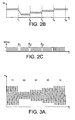
- the operation of the demodulation circuit of the portable object of the Figure 5A is illustrated by the signals shown on the Figures 2A and 2B , in the case where the analog-digital converter 16, low resolution, included in the control loop of the AC voltage Vac across the antenna 10, is constituted by a simple comparator providing a sequence of bits at the frequency of on -échantillonage.
- the control circuit 14 includes an integrator supplying an analog voltage signal Vc representative of the n-bit output signals of the converter 16.
- this signal has the form of a rising voltage ramp when the output of the means 16 is at 1 and a downward voltage ramp when this output is at zero.
- the control voltage V c obtained at the output of the control means 14, is never static.
- the control voltage Vc has the form of a sawtooth signal around a mean level (see FIG. Figure 2B ) proportional to the level of the electromotive force, that is to say proportional to the level of the magnetic field emitted by the fixed station 2 and, therefore, representative of the data transmitted by this fixed station 2.
- the magnetic field H varies between times t 0 and t 5
- the level change of the amplitude of this field H causes a change of level of the electromotive force and, consequently, a rapid variation (decreasing at the instant t 1 and increasing at times t 2 , t 3 and t 4 ) of the AC voltage V ac generated across the antenna 10 and the load impedance 11.
- a decrease in the level of the magnetic field H causes the emission of a sequence of consecutive zeros longer than during the servo-control, causing a decrease in the average amplitude of the control voltage V c .
- an increase in the level of the emitted magnetic field results in the emission of a consecutive sequence of "1", which is longer than during servo-control, causing an increase in the average amplitude of the control voltage.
- V c The number of consecutive O or 1 increases with the amplitude of the jump of the electromotive force.
- the digital output signals of the converter 16 therefore contain information representative of the sign and the amplitude of the variation of the level of the emf generated by the field H, ie information representative of the derivative of the envelope of the electromotive force. or the magnetic field.
- the digital processing circuit 18 therefore comprises at least one digital integration function.
- the integration functions of the circuit of control 14 and / or the digital processing circuit 18 may be implemented by means of integrators and / or low-pass filters.
- the regulation loop of the Figure 5A simultaneously provides part of the analog conversion, which makes the whole more compact.
- the effect of possible slow variations in the mean magnetic field level, due to a movement of the portable object 1 is attenuated by the fact that the output information of the converter 16 is representative of the derivative of the envelope of the magnetic field. Slow variations in the average field level are therefore treated as noise and do not disturb the demodulation.
- the Figure 5B gives an exemplary embodiment of a device according to the invention, for a multi-level demodulation exploiting the calculation of the displacement thresholds for each level.
- Such a device comprises means 50 comparators, for comparing the output of the filter 40 (which is located at the input of the block 18 of digital processing, Figure 5B ) with threshold values from a threshold table 80.
- This threshold table is for example fed during a phase or preamble which includes all the possible displacements, as illustrated on the figure 6 . To all these possible displacements is associated all the corrected or authorized displacements.
- the means 60 are adding means, while the reference 70 designates a register.
- the working frequency is the symbol frequency.
- the threshold table 80 is addressed by the value of the modulation level during the time t n . This value therefore gives the level of modulation that was previously calculated for the moment t n .
- the output of the filter 40 is compared with the thresholds contained in the table 80, and the output of the comparator 50 gives the jump dep (t n + 1 ) according to the logic described above. This jump is added at level level (t n ) to give the level received at time t n + 1 .
- the output of the filter Fir is compared to the thresholds. We then obtain the jumps Dep from which we deduce the level of modulation Niv.
- This example concerns a modulation with 4 levels, noted from 0 to 3, and represented schematically on the Figures 8 and 9 .
- the thresholds for each level are not identical, nor necessarily linearly distributed, and the converter in the transponder is not perfectly linear.
- a transaction between the reader 2 and the transponder 4 then begins, for example, with a preamble, defined in such a way that it contains all the existing relative jumps for all the possible levels.
- the transponder will be able to define all the actual jump thresholds.
- the figure 6 gives an example of a preamble, for the case of 4 levels, issued by the reader 2 before a transaction, making it possible to identify for each level its own thresholds of real jumps.
- Table I indicates, for each T i, the threshold (s) calculated for level (n). ⁇ u> Table I ⁇ / u> Ti Threshold (s) Level (n) T1 -1 3 T2 -1 2 T3 -1 1 T4 +1 0 T5 +1 1 T6 +1 2 T7 -2 3 T8 2 1 T9 -3 3 T10 2 0 T11 -2 2 T12 3 0
- Threshold (T i ) represents the threshold calculated or authorized at time T i (see Table I and figure 7 ).
- the thresholds at -256 are prohibited and are assigned the minimum level (respectively maximum).
- the proposed digital demodulation makes it possible to effectively use the output of a sigma delta converter 20, positioned as illustrated on FIG. Figure 5A (between the input of the converter 16 and an input of the digital processing circuit 18).
- This converter makes it possible to increase the resolution of the demodulation by decreasing the influence of the quantization noise generated by the converter 16.
- the management of different thresholds by level and management (or correction) of the prohibited jumps significantly improve the signal-to-noise ratio and increase the quality of the signal. demodulation.
- a system according to the invention has been realized, with a symbol duration of 1.18 ⁇ s, 4 levels per symbol (ie 2 bits per symbol). Such a system has made it possible to transmit data at 1.7 Mbps.
Landscapes
- Engineering & Computer Science (AREA)
- Computer Networks & Wireless Communication (AREA)
- Computer Hardware Design (AREA)
- Microelectronics & Electronic Packaging (AREA)
- Physics & Mathematics (AREA)
- General Physics & Mathematics (AREA)
- Theoretical Computer Science (AREA)
- Digital Transmission Methods That Use Modulated Carrier Waves (AREA)
- Radar Systems Or Details Thereof (AREA)
- Burglar Alarm Systems (AREA)
- Near-Field Transmission Systems (AREA)
- Input Circuits Of Receivers And Coupling Of Receivers And Audio Equipment (AREA)
Claims (7)
- Verfahren zur Demodulation einer Information, gesendet mittels Amplitudenmodulation durch einen Leser (2) an einen Transponder (4), wobei die Anzahl der Modulationsniveaus größer als oder gleich 2 ist und jedem Madulationsniveau zulässige und vorher eingespeicherte Schwellenwerte zugeordnet sind, umfassend:- einen Schritt zum Vergleichen der Schwankungen einer Rückkopplungs- bzw. Regelungsspannung (Vc) des Transponders (4) und zum Bestimmen eines reellen Werts des Amplitudenmodulationsniveau-Sprungs aufgrund des Resultats dieses Vergleichs,- einen Schritt zum Summieren dieses Sprungs mit einem vorhergehenden ersten Amplitudenmodulationsniveau, um ein zweites Amplitudenmadulationsniveau zu bestimmten.
- Verfahren nach Anspruch 1, das vor jedem Senden des Signals des Lesers (2) an den Transponder (4) das Senden einer alle möglichen Sprünge für alle Modulationsniveaus enthaltenden Präambel umfasst.
- Verfahren nach einem der Ansprüche 1 oder 2, außerdem für jedes Regelungs- bzw. Rückkopplungsspannungsniveau die Berechnung einer neuen Regelungs- bzw. Rückkopplungsspannung (Vc) in Abhängigkeit von dem Niveau der vorhergehenden Spannung und dem zulässigen Schwankungswert.
- Vorrichtung zur Demodulation einer Information, gesendet mittels Amplitudenmodulation durch einen Leser (2) an einen Transponder (4), wobei die Anzahl der Madulationsniveaus größer als oder gleich 2 ist,
dadurch gekennzeichnet, dass sie umfasst:- Einrichtungen (80), um für jedes Niveau der genannten Modulation die aufgrund dieses Niveaus möglichen Schwankungswerte eines Regelungs- bzw. Rückkopplungsspannungssignals des Transponders einzuspeichern,- Einrichtungen (50, 60, 70), um bei jedem Übergang den entsprechenden zulässigen Niveausprung zu berechnen und das neue Regelungs- bzw. Rückkopplungsspannungssignal zu berechnen, in Abhängigkeit von einem vorhergehenden Signalniveau. - Vorrichtung nach Anspruch 4, mit außerdem Antenneneinrichtungen (10), Ladungsimpedanzeinrichtungen (11) an den Anschlüssen der Antenneneinrichtungen und Regelkreiseinrichtungen (12, 16, 14) an den Anschlüssen der Ladungsimpedanzeinrichtungen.
- Vorrichtung nach Anspruch 5, wobei die Regeleinrichtungen Gleichrichtereinrichtungen (12) der Spannung an den Anschlüssen der Antenneneinrichtungen und Steuereinrichtungen (14) zum Modifizieren der Impedanz in Abhängigkeit von dem Ausgang der Gleichrichtereinrichtungen (12) umfassen.
- Vorrichtung nach Anspruch 6, außerdem Demodulationseinrichtungen mit Analog-Digital-Umsetzeinrichtungen (16) zwischen den Steuereinrichtungen (14) und den Gleichrichtereinrichtungen (12) umfassend.
Applications Claiming Priority (1)
| Application Number | Priority Date | Filing Date | Title |
|---|---|---|---|
| FR0550727A FR2883433B1 (fr) | 2005-03-21 | 2005-03-21 | Methode et dispositif de demodulation multiniveaux. |
Publications (2)
| Publication Number | Publication Date |
|---|---|
| EP1705604A1 EP1705604A1 (de) | 2006-09-27 |
| EP1705604B1 true EP1705604B1 (de) | 2009-09-23 |
Family
ID=35064619
Family Applications (1)
| Application Number | Title | Priority Date | Filing Date |
|---|---|---|---|
| EP06111387A Not-in-force EP1705604B1 (de) | 2005-03-21 | 2006-03-20 | Verfahren und Vorrichtung zur Demodulation in mehreren Stufen |
Country Status (6)
| Country | Link |
|---|---|
| US (1) | US7525374B2 (de) |
| EP (1) | EP1705604B1 (de) |
| JP (1) | JP4868903B2 (de) |
| AT (1) | ATE443901T1 (de) |
| DE (1) | DE602006009331D1 (de) |
| FR (1) | FR2883433B1 (de) |
Families Citing this family (9)
| Publication number | Priority date | Publication date | Assignee | Title |
|---|---|---|---|---|
| FR2875976B1 (fr) * | 2004-09-27 | 2006-11-24 | Commissariat Energie Atomique | Dispositif et procede de communication sans contact securisee |
| US7737731B1 (en) | 2005-10-20 | 2010-06-15 | Marvell International Ltd. | High data rate envelope detector for high speed optical storage application |
| WO2008128965A1 (en) * | 2007-04-20 | 2008-10-30 | Cardlab Aps | A portable card with an rfid coil |
| IL193504A (en) * | 2008-08-17 | 2013-02-28 | Michael Braiman | RF coded communication system |
| FR2939580A1 (fr) * | 2008-12-09 | 2010-06-11 | Commissariat Energie Atomique | Objet portatif couple inductivement a une station fixe et comportant des moyens de controle du gain |
| EP3035230A1 (de) | 2014-12-19 | 2016-06-22 | Cardlab ApS | Verfahren und Anordnung zum Erzeugen eines Magnetfeldes |
| MA41187A (fr) | 2014-12-19 | 2021-04-07 | Cardlab Aps | Procédé et ensemble pour générer un champ magnétique et procédé de fabrication d'un ensemble |
| EP3082071A1 (de) | 2015-04-17 | 2016-10-19 | Cardlab ApS | Vorrichtung und verfahren zur ausgabe eines magnetfelds |
| GB2560314B (en) * | 2017-03-06 | 2022-03-30 | Safran Electrical & Power | An electrical machine |
Family Cites Families (8)
| Publication number | Priority date | Publication date | Assignee | Title |
|---|---|---|---|---|
| JPH07123121A (ja) * | 1992-04-02 | 1995-05-12 | Shinko Electric Co Ltd | 復調方式 |
| US5825243A (en) * | 1995-10-30 | 1998-10-20 | Casio Computer Co., Ltd. | Apparatus and method for demodulating multi-level signal |
| JPH10163877A (ja) * | 1996-11-28 | 1998-06-19 | Sony Corp | 復調回路における多値コンパレータのしきい値制御回路 |
| US6078627A (en) * | 1997-12-18 | 2000-06-20 | Advanced Micro Devices, Inc. | Circuit and method for multilevel signal decoding, descrambling, and error detection |
| JP3522745B2 (ja) * | 2000-10-05 | 2004-04-26 | 松下電器産業株式会社 | 伝送路符号化方法、および復号方法 |
| FR2853479A1 (fr) * | 2003-04-07 | 2004-10-08 | Commissariat Energie Atomique | Dispositif de teletransmission par couplage inductif a modulation multiniveaux |
| JP2005012254A (ja) * | 2003-06-16 | 2005-01-13 | Toshiba Tec Corp | 無線通信装置 |
| FR2859842B1 (fr) * | 2003-09-17 | 2006-02-10 | Commissariat Energie Atomique | Objet portatif a demodulation multiniveaux, couple inductivement a une station fixe |
-
2005
- 2005-03-21 FR FR0550727A patent/FR2883433B1/fr not_active Expired - Fee Related
-
2006
- 2006-03-20 EP EP06111387A patent/EP1705604B1/de not_active Not-in-force
- 2006-03-20 DE DE602006009331T patent/DE602006009331D1/de active Active
- 2006-03-20 AT AT06111387T patent/ATE443901T1/de not_active IP Right Cessation
- 2006-03-21 US US11/386,551 patent/US7525374B2/en not_active Expired - Fee Related
- 2006-03-22 JP JP2006078203A patent/JP4868903B2/ja not_active Expired - Fee Related
Also Published As
| Publication number | Publication date |
|---|---|
| JP4868903B2 (ja) | 2012-02-01 |
| US20060225555A1 (en) | 2006-10-12 |
| FR2883433A1 (fr) | 2006-09-22 |
| EP1705604A1 (de) | 2006-09-27 |
| FR2883433B1 (fr) | 2007-04-20 |
| JP2006279956A (ja) | 2006-10-12 |
| ATE443901T1 (de) | 2009-10-15 |
| US7525374B2 (en) | 2009-04-28 |
| DE602006009331D1 (de) | 2009-11-05 |
Similar Documents
| Publication | Publication Date | Title |
|---|---|---|
| EP1705604B1 (de) | Verfahren und Vorrichtung zur Demodulation in mehreren Stufen | |
| EP1459240B1 (de) | Kontaktloser integrierter schaltungsleser mit einem aktiv-bereitschafts-modus mit niedriger stromaufnahme | |
| EP1774458B1 (de) | Ladungsmodulation bei einem elektromagnetischen Transponder | |
| FR2792134A1 (fr) | Detection de distance entre un transpondeur electromagnetique et une borne | |
| CA2245905A1 (fr) | Systeme d'echange de donnees a communication par contacts ou sans contact entre une borne et des objets portatifs | |
| EP1045336A1 (de) | Enggekoppeltes Betriebsverfahren eines elektromagnetischen Transpondersystem | |
| EP1312032A1 (de) | Hochempfindlicher leser für passive transponder | |
| FR2768880A1 (fr) | Demodulateur pour carte a puce sans contact | |
| EP1143377B1 (de) | Aktiver Transponder mit Vorrichtung zur Veränderung der maximalen Kommunikationsdistanz | |
| EP1665573B1 (de) | Tragbares objekt mit mehrebenen-demodulation, das induktiv an eine feststation angekoppelt ist | |
| FR2946821A1 (fr) | Demodulateur adaptatif | |
| FR2636740A1 (fr) | Detecteur d'enveloppe logarithmique de signal analogique | |
| CA2144670C (fr) | Dispositif numerique de recuperation large bande d'une porteuse | |
| WO2001071997A1 (fr) | Demodulateur d'un signal alternatif module en amplitude | |
| EP1705601B1 (de) | Verfahren und Vorrichtung zur Demodulation in zwei Stufen | |
| FR2776781A1 (fr) | Dispositif de controle de l'impedance ramenee sur l'antenne d'une etiquette electromagnetique | |
| EP0473731B1 (de) | Verfahren und anordnung zum vergleich zweier veraenderlicher analogsignale | |
| FR2818784A1 (fr) | Recepteur radiofrequence pour la telereleve de compteurs et methode de telereleve de compteurs comprenant un tel recepteur | |
| CN108933748A (zh) | 实现锁定频率变化的调频信号的解调方法及系统 | |
| EP1335486A1 (de) | Demodulator unter Verwendung von kontaktlosen Chipkarten | |
| EP0541431A1 (de) | Anordnung und Verfahren für die Wiederherstellung eines Taktsignales, angewendet bei der Übertragung von empfangenen Signalen | |
| FR2768881A1 (fr) | Dispositif de commande de l'echantillonnage d'un signal vehiculant des informations binaires codees selon un codage bi-phase | |
| EP1421683A2 (de) | System zur verstärkung eines hochfrequenzsignals und dekodierer für fernsehsignale mit einem solchen system | |
| FR2879378A1 (fr) | Adaptation d'un emetteur en modulation d'amplitude | |
| FR3136121A1 (fr) | Carte sans contact téléalimentée |
Legal Events
| Date | Code | Title | Description |
|---|---|---|---|
| PUAI | Public reference made under article 153(3) epc to a published international application that has entered the european phase |
Free format text: ORIGINAL CODE: 0009012 |
|
| AK | Designated contracting states |
Kind code of ref document: A1 Designated state(s): AT BE BG CH CY CZ DE DK EE ES FI FR GB GR HU IE IS IT LI LT LU LV MC NL PL PT RO SE SI SK TR |
|
| AX | Request for extension of the european patent |
Extension state: AL BA HR MK YU |
|
| RAP1 | Party data changed (applicant data changed or rights of an application transferred) |
Owner name: COMMISSARIAT A L'ENERGIE ATOMIQUE |
|
| 17P | Request for examination filed |
Effective date: 20070316 |
|
| AKX | Designation fees paid |
Designated state(s): AT BE BG CH CY CZ DE DK EE ES FI FR GB GR HU IE IS IT LI LT LU LV MC NL PL PT RO SE SI SK TR |
|
| GRAP | Despatch of communication of intention to grant a patent |
Free format text: ORIGINAL CODE: EPIDOSNIGR1 |
|
| GRAS | Grant fee paid |
Free format text: ORIGINAL CODE: EPIDOSNIGR3 |
|
| GRAA | (expected) grant |
Free format text: ORIGINAL CODE: 0009210 |
|
| AK | Designated contracting states |
Kind code of ref document: B1 Designated state(s): AT BE BG CH CY CZ DE DK EE ES FI FR GB GR HU IE IS IT LI LT LU LV MC NL PL PT RO SE SI SK TR |
|
| REG | Reference to a national code |
Ref country code: GB Ref legal event code: FG4D Free format text: NOT ENGLISH |
|
| REG | Reference to a national code |
Ref country code: CH Ref legal event code: EP |
|
| REG | Reference to a national code |
Ref country code: IE Ref legal event code: FG4D |
|
| REF | Corresponds to: |
Ref document number: 602006009331 Country of ref document: DE Date of ref document: 20091105 Kind code of ref document: P |
|
| PG25 | Lapsed in a contracting state [announced via postgrant information from national office to epo] |
Ref country code: FI Free format text: LAPSE BECAUSE OF FAILURE TO SUBMIT A TRANSLATION OF THE DESCRIPTION OR TO PAY THE FEE WITHIN THE PRESCRIBED TIME-LIMIT Effective date: 20090923 Ref country code: LT Free format text: LAPSE BECAUSE OF FAILURE TO SUBMIT A TRANSLATION OF THE DESCRIPTION OR TO PAY THE FEE WITHIN THE PRESCRIBED TIME-LIMIT Effective date: 20090923 Ref country code: SE Free format text: LAPSE BECAUSE OF FAILURE TO SUBMIT A TRANSLATION OF THE DESCRIPTION OR TO PAY THE FEE WITHIN THE PRESCRIBED TIME-LIMIT Effective date: 20090923 |
|
| LTIE | Lt: invalidation of european patent or patent extension |
Effective date: 20090923 |
|
| PG25 | Lapsed in a contracting state [announced via postgrant information from national office to epo] |
Ref country code: LV Free format text: LAPSE BECAUSE OF FAILURE TO SUBMIT A TRANSLATION OF THE DESCRIPTION OR TO PAY THE FEE WITHIN THE PRESCRIBED TIME-LIMIT Effective date: 20090923 Ref country code: PL Free format text: LAPSE BECAUSE OF FAILURE TO SUBMIT A TRANSLATION OF THE DESCRIPTION OR TO PAY THE FEE WITHIN THE PRESCRIBED TIME-LIMIT Effective date: 20090923 Ref country code: SI Free format text: LAPSE BECAUSE OF FAILURE TO SUBMIT A TRANSLATION OF THE DESCRIPTION OR TO PAY THE FEE WITHIN THE PRESCRIBED TIME-LIMIT Effective date: 20090923 |
|
| NLV1 | Nl: lapsed or annulled due to failure to fulfill the requirements of art. 29p and 29m of the patents act | ||
| PG25 | Lapsed in a contracting state [announced via postgrant information from national office to epo] |
Ref country code: CY Free format text: LAPSE BECAUSE OF FAILURE TO SUBMIT A TRANSLATION OF THE DESCRIPTION OR TO PAY THE FEE WITHIN THE PRESCRIBED TIME-LIMIT Effective date: 20090923 |
|
| REG | Reference to a national code |
Ref country code: IE Ref legal event code: FD4D |
|
| PG25 | Lapsed in a contracting state [announced via postgrant information from national office to epo] |
Ref country code: RO Free format text: LAPSE BECAUSE OF FAILURE TO SUBMIT A TRANSLATION OF THE DESCRIPTION OR TO PAY THE FEE WITHIN THE PRESCRIBED TIME-LIMIT Effective date: 20090923 Ref country code: EE Free format text: LAPSE BECAUSE OF FAILURE TO SUBMIT A TRANSLATION OF THE DESCRIPTION OR TO PAY THE FEE WITHIN THE PRESCRIBED TIME-LIMIT Effective date: 20090923 Ref country code: CZ Free format text: LAPSE BECAUSE OF FAILURE TO SUBMIT A TRANSLATION OF THE DESCRIPTION OR TO PAY THE FEE WITHIN THE PRESCRIBED TIME-LIMIT Effective date: 20090923 Ref country code: PT Free format text: LAPSE BECAUSE OF FAILURE TO SUBMIT A TRANSLATION OF THE DESCRIPTION OR TO PAY THE FEE WITHIN THE PRESCRIBED TIME-LIMIT Effective date: 20100125 Ref country code: ES Free format text: LAPSE BECAUSE OF FAILURE TO SUBMIT A TRANSLATION OF THE DESCRIPTION OR TO PAY THE FEE WITHIN THE PRESCRIBED TIME-LIMIT Effective date: 20100103 Ref country code: IE Free format text: LAPSE BECAUSE OF FAILURE TO SUBMIT A TRANSLATION OF THE DESCRIPTION OR TO PAY THE FEE WITHIN THE PRESCRIBED TIME-LIMIT Effective date: 20090923 Ref country code: IS Free format text: LAPSE BECAUSE OF FAILURE TO SUBMIT A TRANSLATION OF THE DESCRIPTION OR TO PAY THE FEE WITHIN THE PRESCRIBED TIME-LIMIT Effective date: 20100123 |
|
| PG25 | Lapsed in a contracting state [announced via postgrant information from national office to epo] |
Ref country code: SK Free format text: LAPSE BECAUSE OF FAILURE TO SUBMIT A TRANSLATION OF THE DESCRIPTION OR TO PAY THE FEE WITHIN THE PRESCRIBED TIME-LIMIT Effective date: 20090923 |
|
| PG25 | Lapsed in a contracting state [announced via postgrant information from national office to epo] |
Ref country code: AT Free format text: LAPSE BECAUSE OF FAILURE TO SUBMIT A TRANSLATION OF THE DESCRIPTION OR TO PAY THE FEE WITHIN THE PRESCRIBED TIME-LIMIT Effective date: 20090923 |
|
| PG25 | Lapsed in a contracting state [announced via postgrant information from national office to epo] |
Ref country code: NL Free format text: LAPSE BECAUSE OF FAILURE TO SUBMIT A TRANSLATION OF THE DESCRIPTION OR TO PAY THE FEE WITHIN THE PRESCRIBED TIME-LIMIT Effective date: 20090923 Ref country code: DK Free format text: LAPSE BECAUSE OF FAILURE TO SUBMIT A TRANSLATION OF THE DESCRIPTION OR TO PAY THE FEE WITHIN THE PRESCRIBED TIME-LIMIT Effective date: 20090923 |
|
| PLBE | No opposition filed within time limit |
Free format text: ORIGINAL CODE: 0009261 |
|
| STAA | Information on the status of an ep patent application or granted ep patent |
Free format text: STATUS: NO OPPOSITION FILED WITHIN TIME LIMIT |
|
| 26N | No opposition filed |
Effective date: 20100624 |
|
| BERE | Be: lapsed |
Owner name: COMMISSARIAT A L'ENERGIE ATOMIQUE Effective date: 20100331 |
|
| PG25 | Lapsed in a contracting state [announced via postgrant information from national office to epo] |
Ref country code: MC Free format text: LAPSE BECAUSE OF NON-PAYMENT OF DUE FEES Effective date: 20100331 Ref country code: GR Free format text: LAPSE BECAUSE OF FAILURE TO SUBMIT A TRANSLATION OF THE DESCRIPTION OR TO PAY THE FEE WITHIN THE PRESCRIBED TIME-LIMIT Effective date: 20091224 |
|
| REG | Reference to a national code |
Ref country code: CH Ref legal event code: PL |
|
| PG25 | Lapsed in a contracting state [announced via postgrant information from national office to epo] |
Ref country code: BE Free format text: LAPSE BECAUSE OF NON-PAYMENT OF DUE FEES Effective date: 20100331 Ref country code: CH Free format text: LAPSE BECAUSE OF NON-PAYMENT OF DUE FEES Effective date: 20100331 Ref country code: LI Free format text: LAPSE BECAUSE OF NON-PAYMENT OF DUE FEES Effective date: 20100331 |
|
| PG25 | Lapsed in a contracting state [announced via postgrant information from national office to epo] |
Ref country code: LU Free format text: LAPSE BECAUSE OF NON-PAYMENT OF DUE FEES Effective date: 20100320 Ref country code: HU Free format text: LAPSE BECAUSE OF FAILURE TO SUBMIT A TRANSLATION OF THE DESCRIPTION OR TO PAY THE FEE WITHIN THE PRESCRIBED TIME-LIMIT Effective date: 20100324 Ref country code: BG Free format text: LAPSE BECAUSE OF FAILURE TO SUBMIT A TRANSLATION OF THE DESCRIPTION OR TO PAY THE FEE WITHIN THE PRESCRIBED TIME-LIMIT Effective date: 20090923 |
|
| PG25 | Lapsed in a contracting state [announced via postgrant information from national office to epo] |
Ref country code: TR Free format text: LAPSE BECAUSE OF FAILURE TO SUBMIT A TRANSLATION OF THE DESCRIPTION OR TO PAY THE FEE WITHIN THE PRESCRIBED TIME-LIMIT Effective date: 20090923 |
|
| PGFP | Annual fee paid to national office [announced via postgrant information from national office to epo] |
Ref country code: IT Payment date: 20150326 Year of fee payment: 10 |
|
| REG | Reference to a national code |
Ref country code: FR Ref legal event code: PLFP Year of fee payment: 11 |
|
| PG25 | Lapsed in a contracting state [announced via postgrant information from national office to epo] |
Ref country code: IT Free format text: LAPSE BECAUSE OF NON-PAYMENT OF DUE FEES Effective date: 20160320 |
|
| REG | Reference to a national code |
Ref country code: FR Ref legal event code: PLFP Year of fee payment: 12 |
|
| REG | Reference to a national code |
Ref country code: FR Ref legal event code: PLFP Year of fee payment: 13 |
|
| PGFP | Annual fee paid to national office [announced via postgrant information from national office to epo] |
Ref country code: DE Payment date: 20200311 Year of fee payment: 15 Ref country code: GB Payment date: 20200323 Year of fee payment: 15 |
|
| PGFP | Annual fee paid to national office [announced via postgrant information from national office to epo] |
Ref country code: FR Payment date: 20200331 Year of fee payment: 15 |
|
| REG | Reference to a national code |
Ref country code: DE Ref legal event code: R119 Ref document number: 602006009331 Country of ref document: DE |
|
| GBPC | Gb: european patent ceased through non-payment of renewal fee |
Effective date: 20210320 |
|
| PG25 | Lapsed in a contracting state [announced via postgrant information from national office to epo] |
Ref country code: FR Free format text: LAPSE BECAUSE OF NON-PAYMENT OF DUE FEES Effective date: 20210331 Ref country code: GB Free format text: LAPSE BECAUSE OF NON-PAYMENT OF DUE FEES Effective date: 20210320 Ref country code: DE Free format text: LAPSE BECAUSE OF NON-PAYMENT OF DUE FEES Effective date: 20211001 |