EP1665573B1 - Tragbares objekt mit mehrebenen-demodulation, das induktiv an eine feststation angekoppelt ist - Google Patents
Tragbares objekt mit mehrebenen-demodulation, das induktiv an eine feststation angekoppelt ist Download PDFInfo
- Publication number
- EP1665573B1 EP1665573B1 EP04787371A EP04787371A EP1665573B1 EP 1665573 B1 EP1665573 B1 EP 1665573B1 EP 04787371 A EP04787371 A EP 04787371A EP 04787371 A EP04787371 A EP 04787371A EP 1665573 B1 EP1665573 B1 EP 1665573B1
- Authority
- EP
- European Patent Office
- Prior art keywords
- portable object
- converter
- voltage
- fixed station
- data
- Prior art date
- Legal status (The legal status is an assumption and is not a legal conclusion. Google has not performed a legal analysis and makes no representation as to the accuracy of the status listed.)
- Expired - Lifetime
Links
Images




Classifications
-
- H—ELECTRICITY
- H04—ELECTRIC COMMUNICATION TECHNIQUE
- H04B—TRANSMISSION
- H04B5/00—Near-field transmission systems, e.g. inductive or capacitive transmission systems
- H04B5/70—Near-field transmission systems, e.g. inductive or capacitive transmission systems specially adapted for specific purposes
- H04B5/77—Near-field transmission systems, e.g. inductive or capacitive transmission systems specially adapted for specific purposes for interrogation
-
- G—PHYSICS
- G06—COMPUTING OR CALCULATING; COUNTING
- G06K—GRAPHICAL DATA READING; PRESENTATION OF DATA; RECORD CARRIERS; HANDLING RECORD CARRIERS
- G06K19/00—Record carriers for use with machines and with at least a part designed to carry digital markings
- G06K19/06—Record carriers for use with machines and with at least a part designed to carry digital markings characterised by the kind of the digital marking, e.g. shape, nature, code
- G06K19/067—Record carriers with conductive marks, printed circuits or semiconductor circuit elements, e.g. credit or identity cards also with resonating or responding marks without active components
- G06K19/07—Record carriers with conductive marks, printed circuits or semiconductor circuit elements, e.g. credit or identity cards also with resonating or responding marks without active components with integrated circuit chips
- G06K19/0723—Record carriers with conductive marks, printed circuits or semiconductor circuit elements, e.g. credit or identity cards also with resonating or responding marks without active components with integrated circuit chips the record carrier comprising an arrangement for non-contact communication, e.g. wireless communication circuits on transponder cards, non-contact smart cards or RFIDs
-
- G—PHYSICS
- G06—COMPUTING OR CALCULATING; COUNTING
- G06K—GRAPHICAL DATA READING; PRESENTATION OF DATA; RECORD CARRIERS; HANDLING RECORD CARRIERS
- G06K7/00—Methods or arrangements for sensing record carriers, e.g. for reading patterns
- G06K7/0008—General problems related to the reading of electronic memory record carriers, independent of its reading method, e.g. power transfer
Definitions
- the invention relates to a portable object provided with an antenna inductively coupled to a fixed station of a teletransmission device, the portable object comprising a variable load impedance, connected to the terminals of the antenna, and a control loop of the voltage across the load impedance having means for rectifying the voltage across the antenna and control means for changing the load impedance as a function of the output voltage of the rectifying means.
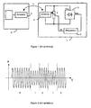
- the inductive coupling is conventionally used for the teletransmission of data between a portable object 1, in particular of the card, ticket or contactless tag type, known as the RFID ("radiofrequency identification") tag. etc., and a fixed station 2, for example consisting of a card reader, a label interrogator, etc., in the field of object identification, access control, electronic toll collection, etc.
- a portable object in particular of the card, ticket or contactless tag type, known as the RFID (“radiofrequency identification") tag. etc.
- RFID radiofrequency identification
- the document WO-A-00/63830 describes a fixed station coupled to a passive, standard RFID tag with variable load impedance.
- the portable object 1 is passive. It is tele-powered by the fixed station 2, which has its own power supply circuit, by means of the inductive coupling which is achieved by antennas 3 and 4, constituted by coils. These devices generally use the principle of charge modulation.
- the transmission of binary data from the fixed station 2 to the portable object 1 is conventionally done, particularly in the document WO-A-00/03352 , by amplitude modulation keying (ASK).
- ASK amplitude modulation keying
- the amplitude of the magnetic field H emitted by the fixed station 2 and received by the portable object 1 takes a first value when the data signal to be transmitted takes the binary value 0 and a second value, lower at the first in FIG. 2, when the data signal to be transmitted takes the binary value 1.
- the antenna 3 of the portable object 1 is the seat of an electromotive force, which creates at the terminals of the antenna 3 an alternating voltage Vac whose amplitude depends, inter alia, on the magnetic field emitted by the fixed station, the load impedance Z connected in parallel on the antenna 3 and the distance between the portable object and the fixed station.
- the latter comprises, as represented in FIG. 1, a rectifying circuit 5, connected to the output of the antenna 3.
- a DC voltage Vdc whose amplitude is representative of the transmitted data, is therefore produced at the output of the rectifying circuit 5, from the voltage at the terminals of the antenna winding 3, induced by the magnetic field emitted by the reader 2.
- the rectifying circuit 5 can be constituted by any suitable circuit for transforming an AC voltage Vac into a DC voltage Vdc. It may, for example, be constituted by one of the circuits shown in FIGS. 3 to 6 and conventionally comprising, respectively, a diode (FIG. 3), a diode bridge (FIG. 4) or single-wave rectification circuits (FIG. 5) or dual-wave rectification circuits (FIG. 6) using MOS-type transistors.
- the magnetic field seen by the portable object 1 varies rapidly with the distance separating the portable object from the reader 2.
- the electromotive force induced in the antenna 3 of the portable object 1 can thus vary in large proportions. Since the portable object 1 essentially consists of an integrated circuit connected to the antenna 3, this circuit is generally protected by means of limiting the voltage at the terminals of the antenna, which makes it possible to use standard low voltage technologies. , less expensive than high voltage technologies. It is known to use for this purpose a shunt-type control circuit, the principle of which is illustrated in FIG. 1.
- the control circuit of FIG. 1 comprises a regulator 6 connected to the output of the rectifying circuit 5 and controlling the value of the load impedance Z, connected to the terminals of the antenna 3, as a function of the output DC voltage Vdc of the rectifying circuit 5.
- the DC voltage Vdc is applied, via a resistor R1, to the source of a PMOS-type transistor T, the drain of which is connected to ground via a resistor R2, while a reference voltage Vref is applied to the gate of the transistor T.
- the regulator thus provides a control voltage Vc, for controlling the value of the impedance
- the PMOS type transistor can be replaced by a bipolar transistor, of the PNP type, or by a JFET type transistor.
- the regulator 6 comprises a divider bridge consisting of two resistors, R3 and R4, connected in series between the output of the rectifier circuit 5 and the ground, and an amplifier 7 having an input (positive in the figure) connected to the midpoint of the divider bridge and another input (negative in the figure) connected to the reference voltage Vref.
- the variable load impedance Z may be constituted by a transistor T, for example of the MOSFET, JFET or bipolar type, the control electrode of which is connected to the output of the regulator 6.
- the voltage Vdc is thus regulated to a dependent value. of the reference voltage Vref, which regulates and limits the voltage across the antenna 3.
- the variable impedance can also be constituted by any other known means, for example by a resistor beam to be connected or disconnected selectively from the antenna 3 as a function of the value of the DC voltage Vdc.
- the object of the invention is a portable object of an inductively coupled teletransmission device making it possible to increase the data rate to be transmitted between the fixed station and the portable object and not having these disadvantages.
- this object is achieved by a portable object according to the appended claims and more particularly by the fact that the fixed station emitting an amplitude-modulated alternating magnetic field over 2 N levels by data to be transmitted, coded on N bits, the portable object comprises demodulation means comprising an n-bit analog-digital converter, clocked at an oversampling frequency much higher than the frequency of the data and connected between the rectifying means and the control means, and digital processing means connected to the output of the converter.
- the device according to the invention uses a multilevel modulation.
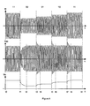
- the amplitude of the alternating magnetic field H emitted by the fixed station 2 is modulated on 2 N levels by data to be transmitted, coded on N bits, with N ⁇ 1.
- N 2-bit words
- the emitted field has a minimum amplitude for transmitting a data item 00 (between times t1 and t3), then takes first and second intermediate values respectively, respectively, to transmit the data 01 respectively (between times t3 and t5) and 10 (between instants t5 and t7), and a maximum value for transmitting data item 11 (between times t0 and t1 and between times t7 and t9).
- a portable object 1 comprising a regulation loop
- the level change of the amplitude of the emitted field causes a change in the level of the electromotive force and, consequently, a rapid variation (decreasing at the instant t1 and increasing at instants t3, t5 and t7) of the amplitude of the AC voltage Vac generated across the antenna 3 and the load impedance Z.
- the regulation loop reacts to this variation by modifying the control voltage Vc of the impedance Z to reduce the amplitude of the voltage Vac to a predetermined regulated value after a transient period whose duration (t1-t2, t3-t4, t5-t6 or t7-t8) depends on the bandwidth of the control loop.
- the level and the variations of the AC voltage Vac are not representative of the levels of the emitted magnetic field corresponding to the binary digital data to be transmitted. This is more particularly evident between instants t3 and t9, corresponding to increasing values of the level of the amplitude of the emitted magnetic field, for which the passage from one level to the next higher level causes the same variations of the voltage Vac.
- the amplitude of the control voltage Vc at the output of the regulation circuit 6 is proportional to the amplitude of the emitted magnetic field.
- the amplitude of the control voltage Vc is therefore representative of the level of the amplitude of the emitted magnetic field and, consequently, of the data to be transmitted.
- the portable object represented in FIG. 10 uses the control voltage Vc to perform multilevel demodulation of the data transmitted between the fixed station 2 and the portable object.
- This portable object is distinguished from the portable object according to FIG. 1 by the addition of an N-bit analog-to-digital converter 8 (A / N), the input of which is connected to the output of the regulator 6 and which provides at the output the demodulated data in the form of words of N bits.
- the variations of the control voltage Vc are small, especially when the variable load impedance Z is constituted by a transistor of the M OS type whose gate is connected to the output of the regulator 6.
- the voltage of Vc control then varies between the threshold voltage of the transistor and the threshold voltage plus a few hundred millivolts. This imposes a strong resolution of the converter analog-digital 8, which can cause problems in terms of its consumption and the silicon surface required.
- the analog-digital converter 8 then being connected to the output of a current measuring interface.
- the variations of this current are significantly higher than those of the control voltage Vc.
- a complete range of distances may, for example, typically correspond to currents ranging from a few microamperes to a few tens of milliamperes.
- This very large dynamic requires a very high resolution of the analog-digital converter 8 and / or the addition of a system to overcome the distance between the portable object 1 and the fixed station 2.
- a system comprising including automatic gain control circuits and / or automatic range selection, makes the demodulation circuit of the portable object more complex.
- an n-bit analog-to-digital converter 9 (A / N) is introduced into the regulation loop, between the rectifying circuit 5 and a control circuit 10 supplying the control voltage Vc, intended to control the impedance
- N ⁇ 2 and n ⁇ N.
- the oversampling frequency is determined by a clock circuit providing clock signals Ck to a clock input of the converter 9.
- the frequency over-sampling can advantageously be between 10 and 20 MHz.
- the digital output signals of the converter 9 contain the information necessary for the recovery of the data transmitted by the fixed station 2, these digital signals are not directly exploitable.
- the output of the converter 9, connected to the control circuit 10, is, therefore, further connected to the input of a digital processing circuit 11 intended to supply, on N bits, the demodulated data.
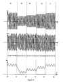
- the operation of the demodulation circuit of the portable object of FIG. 11 is illustrated by the signals represented in FIG. 12, in the case where the analog-digital converter 9, which is low resolution, is included in the voltage regulation loop.
- the control circuit 1 0 is constituted by an integrator supplying an analog voltage signal Vc representative of the n-bit output signals of the converter, for example in the form of a rising voltage ramp when the output of the converter 9 is at 1 and a downward voltage ramp when this output is zero.
- the control voltage Vc obtained at the output of the control circuit 10, is never static.
- the control voltage Vc has the form of a sawtooth signal around a mean level proportional to the level of the electromotive force. , that is, proportional to the level of the emitted magnetic field by the fixed station 2 and, therefore, representative of the data transmitted by the fixed station.
- the magnetic field H varies between the instants t0 and t9 in the same manner as in FIG. 9.
- the level change of the amplitude of the magnetic field H emitted causes a change of level of the electromotive force and, consequently, a rapid variation (decreasing at time t1 and increasing at times t3, t5 and t7) of the alternating voltage Vac generated at the terminals of antenna 3 and the load impedance Z
- the digital output of the converter 9, which compares the amplitude of the rectified voltage to a predetermined threshold, is then constituted by a series of bits at the oversampling frequency and, more particularly, by an alternation of pairs of 0 and of pairs of 1: 1100110011 001100 between times t0 and t1, 0000001100110011 between times t1 and t3, 1100110011001100 between times t3 and t5, 1111001100110011 between times t5 and t7 and 1100110011001100 between times t5
- a decrease in the level of the emitted magnetic field therefore results (for example at time t1) by the emission of more than two consecutive 0, thus causing a decrease in the average amplitude of the control voltage Vc.
- an increase in the level of the emitted magnetic field results (for example at times t3, t5 and t7) by the emission of more than two consecutive 1, causing an increase in the average amplitude of the control voltage Vc .
- the number of consecutive 0s or 1s increases with the amplitude of the jump of the electromotive force.
- the digital output signals of the converter 9 thus contain information representative of the sign and the amplitude of the variation of the level of the electromotive force generated by the emitted magnetic field, in other words an information representative of the derivative of the envelope of the electromotive force or magnetic field.
- the integration functions of the control circuit 10 and / or the digital processing circuit 11 can be realized by means of integrators and / or low-pass filters.
- the control loop simultaneously provides part of the analog-digital conversion, which makes the whole more compact.
- the effect of possible slow variations in the mean magnetic field level, due to a movement of the portable object 1 is attenuated by the fact that the output information of the converter 9 is representative of the derivative of the envelope of the magnetic field. Slow variations in the average field level are therefore treated as noise and do not disturb the demodulation.
- the postponement of part of the digital processing in the digital processing circuit is also advantageous.
- the load impedance Z is permanently modulated, even at constant field, and this can disturb the communication in the opposite direction, between the portable object and the fixed station. This disadvantage can nevertheless be avoided by an inhibition of the regulation loop during the transmission of data modulated by the portable object.
- control circuit 10 for example the slope of the ramps of the control voltage Vc, to the mean magnetic field by means of a loop. bandwidth much narrower than that of the main control loop.
- FIG. 13 makes it possible to increase the resolution of the demodulation by decreasing the influence of the quantization noise generated by the converter.
- analog-digital 9 low resolution.
- a sigma-delta type modulator 12 is connected between the input of the analog-digital converter 9 and an additional input of the digital processing circuit 11.
- the input of the converter 9 (rectified voltage Vdc) is thus converted.
- the modulator 12 to an oversampled binary signal and this oversampled binary signal is combined with the output of the converter 9 in the digital processing circuit to provide the demodulated data as N-bit words.
Landscapes
- Engineering & Computer Science (AREA)
- General Physics & Mathematics (AREA)
- Computer Networks & Wireless Communication (AREA)
- Theoretical Computer Science (AREA)
- Physics & Mathematics (AREA)
- Microelectronics & Electronic Packaging (AREA)
- Computer Hardware Design (AREA)
- Artificial Intelligence (AREA)
- Computer Vision & Pattern Recognition (AREA)
- Signal Processing (AREA)
- Near-Field Transmission Systems (AREA)
- Burglar Alarm Systems (AREA)
- Geophysics And Detection Of Objects (AREA)
- Mobile Radio Communication Systems (AREA)
Claims (10)
- Vorrichtung zur Fernübertragung, die eine Feststation (2) und ein tragbares Element umfasst, das eine Antenne (3) aufweist, die induktiv an die Feststation gekoppelt ist, wobei das tragbare Element (1) eine variable Lastimpedanz (Z) umfasst, die an die Klemmen der Antenne (3) gelegt ist, sowie eine Spannungsregelschleife (Vac) an den Klemmen der Lastimpedanz (Z), die Mittel (5) zur Gleichrichtung der Spannung (Vac) an den Klemmen der Antenne und Steuerungsmittel (10) umfasst, die vorgesehen sind, die Lastimpedanz (Z) abhängig von der Ausgangsspannung (Vdc) der Gleichrichtungsmittel (5) zu verändern, Element, das dadurch gekennzeichnet ist, dass die Feststation (2) ein alternatives Magnetfeld (H) aussendet, das auf 2N Ebenen amplitudenmoduliert ist, und zwar durch zu übermittelnde Daten, die auf N Bit kodiert sind, und dass das tragbare Element (1) Demodulationsmittel umfasst, die einen n Bit-Analog-Digital-Umsetzer (9) umfassen, der auf eine Überabtastungsfrequenz (Ck) getaktet sind, die weit über der Frequenz der Daten liegt und zwischen die Gleichrichtungsmittel (5) und die Steuerungsmittel (10) geschaltet sind, sowie digitale Verarbeitungsmittel (11), die an den Ausgang des Wandlers (9) gelegt sind.
- Vorrichtung nach Anspruch 1, dadurch gekennzeichnet, dass die jeweiligen Werte von N und n so vorgesehen sind, dass N ≥ 2 und n < N.
- Vorrichtung nach einem der Ansprüche 1 und 2, dadurch gekennzeichnet, dass die digitale Verarbeitungsmittel (11) digitale Integrationsmittel umfassen, welche Signale mit N Bit liefern, die für die übermittelten Daten stehen.
- Vorrichtung nach einem der Ansprüche 1 bis 3, dadurch gekennzeichnet, dass die Steuerungsmittel (10) Integrationsmittel umfassen, die ein analoges Spannungssignal (Vc) liefern, das für die n Bit-Ausgangssignale des Wandlers steht.
- Vorrichtung nach Anspruch 4, dadurch gekennzeichnet, dass die Integrationsmittel einen Tiefpassfilter umfassen.
- Vorrichtung nach einem der Ansprüche 1 bis 5, dadurch gekennzeichnet, dass n = 1.
- Vorrichtung nach Anspruch 6, dadurch gekennzeichnet, dass der Wandler (9) ein Komparator ist.
- Vorrichtung nach einem der Ansprüche 1 bis 7, dadurch gekennzeichnet, dass N = 2.
- Vorrichtung nach einem der Ansprüche 1 bis 8, dadurch gekennzeichnet, dass die variable Impedanz (Z) einen MOS-Transistor umfasst.
- Vorrichtung nach einem der Ansprüche 1 bis 9, dadurch gekennzeichnet, dass sie einen Sigma-Delta-Modulator (12) umfasst, der zwischen den Eingang des Analog-Digital-Umsetzers (9) und einen zusätzlichen Eingang der digitale Verarbeitungsmittel (11) geschaltet ist.
Applications Claiming Priority (2)
| Application Number | Priority Date | Filing Date | Title |
|---|---|---|---|
| FR0310928A FR2859842B1 (fr) | 2003-09-17 | 2003-09-17 | Objet portatif a demodulation multiniveaux, couple inductivement a une station fixe |
| PCT/FR2004/002325 WO2005029726A1 (fr) | 2003-09-17 | 2004-09-14 | Objet portatif à démodulation multiniveaux, couplé inductivement à une station fixe |
Publications (2)
| Publication Number | Publication Date |
|---|---|
| EP1665573A1 EP1665573A1 (de) | 2006-06-07 |
| EP1665573B1 true EP1665573B1 (de) | 2008-01-09 |
Family
ID=34203521
Family Applications (1)
| Application Number | Title | Priority Date | Filing Date |
|---|---|---|---|
| EP04787371A Expired - Lifetime EP1665573B1 (de) | 2003-09-17 | 2004-09-14 | Tragbares objekt mit mehrebenen-demodulation, das induktiv an eine feststation angekoppelt ist |
Country Status (7)
| Country | Link |
|---|---|
| US (1) | US7575165B2 (de) |
| EP (1) | EP1665573B1 (de) |
| JP (1) | JP4708346B2 (de) |
| AT (1) | ATE383680T1 (de) |
| DE (1) | DE602004011240T2 (de) |
| FR (1) | FR2859842B1 (de) |
| WO (1) | WO2005029726A1 (de) |
Families Citing this family (11)
| Publication number | Priority date | Publication date | Assignee | Title |
|---|---|---|---|---|
| CN100438271C (zh) * | 2004-01-30 | 2008-11-26 | 株式会社瑞萨科技 | 半导体集成电路器件和使用它的非接触式ic卡以及便携式信息终端 |
| FR2875976B1 (fr) * | 2004-09-27 | 2006-11-24 | Commissariat Energie Atomique | Dispositif et procede de communication sans contact securisee |
| FR2883433B1 (fr) * | 2005-03-21 | 2007-04-20 | Commissariat Energie Atomique | Methode et dispositif de demodulation multiniveaux. |
| FR2883434B1 (fr) * | 2005-03-21 | 2007-04-20 | Commissariat Energie Atomique | Methode et dispositif de demodulation a deux niveaux. |
| JP2007036216A (ja) | 2005-06-24 | 2007-02-08 | Semiconductor Energy Lab Co Ltd | 半導体装置及び無線通信システム |
| DE102006048594B4 (de) * | 2006-10-13 | 2009-07-30 | Infineon Technologies Ag | Schaltungsanordnung zum kontaktlosen Datenaustausch und Chipkarte |
| IL187035A0 (en) * | 2007-10-30 | 2008-02-09 | Sandisk Il Ltd | Configurable random number generator |
| FR2939580A1 (fr) * | 2008-12-09 | 2010-06-11 | Commissariat Energie Atomique | Objet portatif couple inductivement a une station fixe et comportant des moyens de controle du gain |
| US8643356B2 (en) | 2009-10-06 | 2014-02-04 | Infineon Technologies Ag | Voltage regulation and modulation circuit |
| KR102494550B1 (ko) * | 2016-10-12 | 2023-02-02 | 주식회사 위츠 | 정보 송신 장치 |
| USD1013170S1 (en) | 2020-10-29 | 2024-01-30 | Cilag Gmbh International | Surgical instrument assembly |
Family Cites Families (11)
| Publication number | Priority date | Publication date | Assignee | Title |
|---|---|---|---|---|
| JPH087059A (ja) * | 1994-06-21 | 1996-01-12 | Sony Chem Corp | 非接触情報カード |
| JP3392016B2 (ja) * | 1996-09-13 | 2003-03-31 | 株式会社日立製作所 | 電力伝送システム並びに電力伝送および情報通信システム |
| EP0871897A1 (de) * | 1996-11-05 | 1998-10-21 | Koninklijke Philips Electronics N.V. | Kontaktlose datenübertragung und empfangsgerät mit synchrondemodulator |
| US6501807B1 (en) * | 1998-02-06 | 2002-12-31 | Intermec Ip Corp. | Data recovery system for radio frequency identification interrogator |
| WO2000003352A1 (en) * | 1998-07-10 | 2000-01-20 | Intermec Ip Corp. | Apparatus and method for recovering data signals sent to rf tags |
| JP3488166B2 (ja) * | 2000-02-24 | 2004-01-19 | 日本電信電話株式会社 | 非接触icカードシステムとそのリーダライタおよび非接触icカード |
| JP3650317B2 (ja) * | 2000-08-23 | 2005-05-18 | 日本電信電話株式会社 | 電磁場受信装置 |
| US20050225436A1 (en) * | 2004-04-13 | 2005-10-13 | Diorio Christopher J | Method and system to calibrate an oscillator within an RFID circuit responsive to a received update value |
| US20080186138A1 (en) * | 2005-12-09 | 2008-08-07 | Butler Timothy P | Methods and systems of a multiple radio frequency network node rfid tag |
| JP5148504B2 (ja) * | 2005-12-09 | 2013-02-20 | テゴ,インコーポレイテッド | 多重無線周波数ネットワークノードrfidタグ |
| DE102006048594B4 (de) * | 2006-10-13 | 2009-07-30 | Infineon Technologies Ag | Schaltungsanordnung zum kontaktlosen Datenaustausch und Chipkarte |
-
2003
- 2003-09-17 FR FR0310928A patent/FR2859842B1/fr not_active Expired - Fee Related
-
2004
- 2004-09-14 US US10/570,267 patent/US7575165B2/en not_active Expired - Fee Related
- 2004-09-14 EP EP04787371A patent/EP1665573B1/de not_active Expired - Lifetime
- 2004-09-14 WO PCT/FR2004/002325 patent/WO2005029726A1/fr not_active Ceased
- 2004-09-14 DE DE602004011240T patent/DE602004011240T2/de not_active Expired - Lifetime
- 2004-09-14 AT AT04787371T patent/ATE383680T1/de not_active IP Right Cessation
- 2004-09-14 JP JP2006526661A patent/JP4708346B2/ja not_active Expired - Fee Related
Also Published As
| Publication number | Publication date |
|---|---|
| ATE383680T1 (de) | 2008-01-15 |
| FR2859842A1 (fr) | 2005-03-18 |
| EP1665573A1 (de) | 2006-06-07 |
| DE602004011240T2 (de) | 2009-01-15 |
| US20060281405A1 (en) | 2006-12-14 |
| JP2007506320A (ja) | 2007-03-15 |
| JP4708346B2 (ja) | 2011-06-22 |
| DE602004011240D1 (de) | 2008-02-21 |
| US7575165B2 (en) | 2009-08-18 |
| FR2859842B1 (fr) | 2006-02-10 |
| WO2005029726A1 (fr) | 2005-03-31 |
Similar Documents
| Publication | Publication Date | Title |
|---|---|---|
| CA2245912C (fr) | Systeme d'echange de donnees par communication sans contact entre une borne et des objets portatifs telealimentes | |
| EP0903689A1 (de) | Demodulator für kontaktlose Chipkarte | |
| FR2859842A1 (fr) | Objet portatif a demodulation multiniveaux, couple inductivement a une station fixe | |
| EP1369813B1 (de) | Lesegerät für einen elektromagnetischen Transponder | |
| FR2792137A1 (fr) | Detection, par un lecteur de transpondeur electromagnetique, de la distance qui le separe d'un transpondeur | |
| EP1705604B1 (de) | Verfahren und Vorrichtung zur Demodulation in mehreren Stufen | |
| WO2004093341A1 (fr) | Dispositif et teletransmission par couplage inductif a modulation multi-niveaux | |
| WO1999050930A1 (fr) | Dispositif de controle de l'impedance ramenee sur l'antenne d'une etiquette electronique | |
| EP1269702A1 (de) | Demodulator für ein amplitudenmoduliertes alternierendes signal | |
| EP3648362A1 (de) | Verfahren zur beschränkung des über einen transponder empfangenen spannungsniveaus aus einem magnetfeld, und entsprechender transponder | |
| EP1152257A1 (de) | Verbesserung der Kapazität der Demodulation eines elektromagnetischen Transponders | |
| FR2835119A1 (fr) | Demodulateur a large dynamique pour cartes a puce ou etiquettes sans contact | |
| FR2917557A1 (fr) | Dispositif de demodulation d'un signal comportant des informations transitant par modulation de la phase d'une porteuse | |
| EP2747277B1 (de) | Demodulationsvorrichtung | |
| FR2676297A1 (fr) | Systeme d'interface comportant un circuit de commande de courants electriques pour la transmission sans contact de donnees et d'energie. | |
| FR3136121A1 (fr) | Carte sans contact téléalimentée | |
| EP2196948B1 (de) | Tragbares Objekt, das induktiv an eine feste Station gekoppelt ist und Mittel zur Verstärkungskontrolle umfasst | |
| FR2801746A1 (fr) | Dispositif d'alimentation stabilisee de composants electroniques tele-alimentes | |
| EP0903688A1 (de) | Radiofrequenzsignaldetektor für kontaktlose IC-Karte | |
| EP1705601B1 (de) | Verfahren und Vorrichtung zur Demodulation in zwei Stufen | |
| EP1471366B1 (de) | RF Sende-Empfänger-Vorrichtung | |
| EP1039408A1 (de) | Fernspeisung für einen elektromagnetischen Transponder | |
| FR2792133A1 (fr) | Regulation de phase d'un lecteur de transpondeurs electromagnetiques | |
| FR2999829A1 (fr) | Equipement electrique adapte a etre connecte a un compteur d'energie electrique |
Legal Events
| Date | Code | Title | Description |
|---|---|---|---|
| PUAI | Public reference made under article 153(3) epc to a published international application that has entered the european phase |
Free format text: ORIGINAL CODE: 0009012 |
|
| 17P | Request for examination filed |
Effective date: 20060222 |
|
| AK | Designated contracting states |
Kind code of ref document: A1 Designated state(s): AT BE BG CH CY CZ DE DK EE ES FI FR GB GR HU IE IT LI LU MC NL PL PT RO SE SI SK TR |
|
| DAX | Request for extension of the european patent (deleted) | ||
| RIN1 | Information on inventor provided before grant (corrected) |
Inventor name: DELORME, NICOLAS Inventor name: VILLARD, PATRICK Inventor name: CONDEMINE, CYRIL |
|
| GRAP | Despatch of communication of intention to grant a patent |
Free format text: ORIGINAL CODE: EPIDOSNIGR1 |
|
| GRAS | Grant fee paid |
Free format text: ORIGINAL CODE: EPIDOSNIGR3 |
|
| GRAA | (expected) grant |
Free format text: ORIGINAL CODE: 0009210 |
|
| AK | Designated contracting states |
Kind code of ref document: B1 Designated state(s): AT BE BG CH CY CZ DE DK EE ES FI FR GB GR HU IE IT LI LU MC NL PL PT RO SE SI SK TR |
|
| REG | Reference to a national code |
Ref country code: GB Ref legal event code: FG4D Free format text: NOT ENGLISH |
|
| REG | Reference to a national code |
Ref country code: CH Ref legal event code: EP |
|
| REG | Reference to a national code |
Ref country code: IE Ref legal event code: FG4D Free format text: LANGUAGE OF EP DOCUMENT: FRENCH |
|
| REF | Corresponds to: |
Ref document number: 602004011240 Country of ref document: DE Date of ref document: 20080221 Kind code of ref document: P |
|
| GBT | Gb: translation of ep patent filed (gb section 77(6)(a)/1977) |
Effective date: 20080408 |
|
| PG25 | Lapsed in a contracting state [announced via postgrant information from national office to epo] |
Ref country code: SI Free format text: LAPSE BECAUSE OF FAILURE TO SUBMIT A TRANSLATION OF THE DESCRIPTION OR TO PAY THE FEE WITHIN THE PRESCRIBED TIME-LIMIT Effective date: 20080109 Ref country code: NL Free format text: LAPSE BECAUSE OF FAILURE TO SUBMIT A TRANSLATION OF THE DESCRIPTION OR TO PAY THE FEE WITHIN THE PRESCRIBED TIME-LIMIT Effective date: 20080109 |
|
| NLV1 | Nl: lapsed or annulled due to failure to fulfill the requirements of art. 29p and 29m of the patents act | ||
| PG25 | Lapsed in a contracting state [announced via postgrant information from national office to epo] |
Ref country code: FI Free format text: LAPSE BECAUSE OF FAILURE TO SUBMIT A TRANSLATION OF THE DESCRIPTION OR TO PAY THE FEE WITHIN THE PRESCRIBED TIME-LIMIT Effective date: 20080109 Ref country code: ES Free format text: LAPSE BECAUSE OF FAILURE TO SUBMIT A TRANSLATION OF THE DESCRIPTION OR TO PAY THE FEE WITHIN THE PRESCRIBED TIME-LIMIT Effective date: 20080420 |
|
| PG25 | Lapsed in a contracting state [announced via postgrant information from national office to epo] |
Ref country code: BG Free format text: LAPSE BECAUSE OF FAILURE TO SUBMIT A TRANSLATION OF THE DESCRIPTION OR TO PAY THE FEE WITHIN THE PRESCRIBED TIME-LIMIT Effective date: 20080409 Ref country code: AT Free format text: LAPSE BECAUSE OF FAILURE TO SUBMIT A TRANSLATION OF THE DESCRIPTION OR TO PAY THE FEE WITHIN THE PRESCRIBED TIME-LIMIT Effective date: 20080109 |
|
| PG25 | Lapsed in a contracting state [announced via postgrant information from national office to epo] |
Ref country code: PL Free format text: LAPSE BECAUSE OF FAILURE TO SUBMIT A TRANSLATION OF THE DESCRIPTION OR TO PAY THE FEE WITHIN THE PRESCRIBED TIME-LIMIT Effective date: 20080109 Ref country code: PT Free format text: LAPSE BECAUSE OF FAILURE TO SUBMIT A TRANSLATION OF THE DESCRIPTION OR TO PAY THE FEE WITHIN THE PRESCRIBED TIME-LIMIT Effective date: 20080609 |
|
| REG | Reference to a national code |
Ref country code: IE Ref legal event code: FD4D |
|
| PG25 | Lapsed in a contracting state [announced via postgrant information from national office to epo] |
Ref country code: SE Free format text: LAPSE BECAUSE OF FAILURE TO SUBMIT A TRANSLATION OF THE DESCRIPTION OR TO PAY THE FEE WITHIN THE PRESCRIBED TIME-LIMIT Effective date: 20080409 Ref country code: DK Free format text: LAPSE BECAUSE OF FAILURE TO SUBMIT A TRANSLATION OF THE DESCRIPTION OR TO PAY THE FEE WITHIN THE PRESCRIBED TIME-LIMIT Effective date: 20080109 Ref country code: SK Free format text: LAPSE BECAUSE OF FAILURE TO SUBMIT A TRANSLATION OF THE DESCRIPTION OR TO PAY THE FEE WITHIN THE PRESCRIBED TIME-LIMIT Effective date: 20080109 Ref country code: CZ Free format text: LAPSE BECAUSE OF FAILURE TO SUBMIT A TRANSLATION OF THE DESCRIPTION OR TO PAY THE FEE WITHIN THE PRESCRIBED TIME-LIMIT Effective date: 20080109 Ref country code: IE Free format text: LAPSE BECAUSE OF FAILURE TO SUBMIT A TRANSLATION OF THE DESCRIPTION OR TO PAY THE FEE WITHIN THE PRESCRIBED TIME-LIMIT Effective date: 20080109 |
|
| PLBE | No opposition filed within time limit |
Free format text: ORIGINAL CODE: 0009261 |
|
| STAA | Information on the status of an ep patent application or granted ep patent |
Free format text: STATUS: NO OPPOSITION FILED WITHIN TIME LIMIT |
|
| PG25 | Lapsed in a contracting state [announced via postgrant information from national office to epo] |
Ref country code: RO Free format text: LAPSE BECAUSE OF FAILURE TO SUBMIT A TRANSLATION OF THE DESCRIPTION OR TO PAY THE FEE WITHIN THE PRESCRIBED TIME-LIMIT Effective date: 20080109 |
|
| 26N | No opposition filed |
Effective date: 20081010 |
|
| BERE | Be: lapsed |
Owner name: COMMISSARIAT A L'ENERGIE ATOMIQUE Effective date: 20080930 |
|
| PG25 | Lapsed in a contracting state [announced via postgrant information from national office to epo] |
Ref country code: EE Free format text: LAPSE BECAUSE OF FAILURE TO SUBMIT A TRANSLATION OF THE DESCRIPTION OR TO PAY THE FEE WITHIN THE PRESCRIBED TIME-LIMIT Effective date: 20080109 Ref country code: MC Free format text: LAPSE BECAUSE OF NON-PAYMENT OF DUE FEES Effective date: 20080930 |
|
| REG | Reference to a national code |
Ref country code: CH Ref legal event code: PL |
|
| PG25 | Lapsed in a contracting state [announced via postgrant information from national office to epo] |
Ref country code: BE Free format text: LAPSE BECAUSE OF NON-PAYMENT OF DUE FEES Effective date: 20080930 Ref country code: CY Free format text: LAPSE BECAUSE OF FAILURE TO SUBMIT A TRANSLATION OF THE DESCRIPTION OR TO PAY THE FEE WITHIN THE PRESCRIBED TIME-LIMIT Effective date: 20080109 |
|
| PG25 | Lapsed in a contracting state [announced via postgrant information from national office to epo] |
Ref country code: LI Free format text: LAPSE BECAUSE OF NON-PAYMENT OF DUE FEES Effective date: 20080930 Ref country code: CH Free format text: LAPSE BECAUSE OF NON-PAYMENT OF DUE FEES Effective date: 20080930 |
|
| PG25 | Lapsed in a contracting state [announced via postgrant information from national office to epo] |
Ref country code: HU Free format text: LAPSE BECAUSE OF FAILURE TO SUBMIT A TRANSLATION OF THE DESCRIPTION OR TO PAY THE FEE WITHIN THE PRESCRIBED TIME-LIMIT Effective date: 20080710 Ref country code: LU Free format text: LAPSE BECAUSE OF NON-PAYMENT OF DUE FEES Effective date: 20080914 |
|
| PG25 | Lapsed in a contracting state [announced via postgrant information from national office to epo] |
Ref country code: TR Free format text: LAPSE BECAUSE OF FAILURE TO SUBMIT A TRANSLATION OF THE DESCRIPTION OR TO PAY THE FEE WITHIN THE PRESCRIBED TIME-LIMIT Effective date: 20080109 |
|
| PG25 | Lapsed in a contracting state [announced via postgrant information from national office to epo] |
Ref country code: GR Free format text: LAPSE BECAUSE OF FAILURE TO SUBMIT A TRANSLATION OF THE DESCRIPTION OR TO PAY THE FEE WITHIN THE PRESCRIBED TIME-LIMIT Effective date: 20080410 |
|
| PGFP | Annual fee paid to national office [announced via postgrant information from national office to epo] |
Ref country code: IT Payment date: 20140915 Year of fee payment: 11 |
|
| PG25 | Lapsed in a contracting state [announced via postgrant information from national office to epo] |
Ref country code: IT Free format text: LAPSE BECAUSE OF NON-PAYMENT OF DUE FEES Effective date: 20150914 |
|
| REG | Reference to a national code |
Ref country code: FR Ref legal event code: PLFP Year of fee payment: 13 |
|
| PGFP | Annual fee paid to national office [announced via postgrant information from national office to epo] |
Ref country code: GB Payment date: 20160916 Year of fee payment: 13 Ref country code: DE Payment date: 20160914 Year of fee payment: 13 |
|
| PGFP | Annual fee paid to national office [announced via postgrant information from national office to epo] |
Ref country code: FR Payment date: 20160928 Year of fee payment: 13 |
|
| REG | Reference to a national code |
Ref country code: DE Ref legal event code: R119 Ref document number: 602004011240 Country of ref document: DE |
|
| GBPC | Gb: european patent ceased through non-payment of renewal fee |
Effective date: 20170914 |
|
| REG | Reference to a national code |
Ref country code: FR Ref legal event code: ST Effective date: 20180531 |
|
| PG25 | Lapsed in a contracting state [announced via postgrant information from national office to epo] |
Ref country code: GB Free format text: LAPSE BECAUSE OF NON-PAYMENT OF DUE FEES Effective date: 20170914 Ref country code: DE Free format text: LAPSE BECAUSE OF NON-PAYMENT OF DUE FEES Effective date: 20180404 |
|
| PG25 | Lapsed in a contracting state [announced via postgrant information from national office to epo] |
Ref country code: FR Free format text: LAPSE BECAUSE OF NON-PAYMENT OF DUE FEES Effective date: 20171002 |