EP1703567A2 - Feldeffekttransistor mit isoliertem Gate und Verfahren zu dessen Herstellung - Google Patents
Feldeffekttransistor mit isoliertem Gate und Verfahren zu dessen Herstellung Download PDFInfo
- Publication number
- EP1703567A2 EP1703567A2 EP06005521A EP06005521A EP1703567A2 EP 1703567 A2 EP1703567 A2 EP 1703567A2 EP 06005521 A EP06005521 A EP 06005521A EP 06005521 A EP06005521 A EP 06005521A EP 1703567 A2 EP1703567 A2 EP 1703567A2
- Authority
- EP
- European Patent Office
- Prior art keywords
- gate electrode
- region
- conductivity type
- channel regions
- general conductivity
- Prior art date
- Legal status (The legal status is an assumption and is not a legal conclusion. Google has not performed a legal analysis and makes no representation as to the accuracy of the status listed.)
- Withdrawn
Links
- 238000004519 manufacturing process Methods 0.000 title claims description 20
- 230000005669 field effect Effects 0.000 title 1
- 239000012535 impurity Substances 0.000 claims abstract description 137
- 239000000758 substrate Substances 0.000 claims abstract description 45
- 239000004065 semiconductor Substances 0.000 claims description 98
- 238000000926 separation method Methods 0.000 claims description 30
- 238000000034 method Methods 0.000 claims description 12
- 230000015572 biosynthetic process Effects 0.000 claims description 9
- 238000009792 diffusion process Methods 0.000 claims description 9
- 238000009413 insulation Methods 0.000 claims description 4
- 238000005468 ion implantation Methods 0.000 claims description 4
- 238000010438 heat treatment Methods 0.000 claims description 2
- 230000015556 catabolic process Effects 0.000 abstract description 20
- 108091006146 Channels Proteins 0.000 description 92
- 239000010410 layer Substances 0.000 description 69
- 239000011229 interlayer Substances 0.000 description 11
- 238000007669 thermal treatment Methods 0.000 description 9
- 229920002120 photoresistant polymer Polymers 0.000 description 7
- OAICVXFJPJFONN-UHFFFAOYSA-N Phosphorus Chemical compound [P] OAICVXFJPJFONN-UHFFFAOYSA-N 0.000 description 6
- ZOXJGFHDIHLPTG-UHFFFAOYSA-N Boron Chemical compound [B] ZOXJGFHDIHLPTG-UHFFFAOYSA-N 0.000 description 5
- 230000001133 acceleration Effects 0.000 description 5
- 229910052796 boron Inorganic materials 0.000 description 5
- 229910021420 polycrystalline silicon Inorganic materials 0.000 description 5
- 229920005591 polysilicon Polymers 0.000 description 5
- 108010075750 P-Type Calcium Channels Proteins 0.000 description 4
- XUIMIQQOPSSXEZ-UHFFFAOYSA-N Silicon Chemical compound [Si] XUIMIQQOPSSXEZ-UHFFFAOYSA-N 0.000 description 4
- 238000010030 laminating Methods 0.000 description 4
- 229910052710 silicon Inorganic materials 0.000 description 4
- 239000010703 silicon Substances 0.000 description 4
- 150000002500 ions Chemical class 0.000 description 3
- 230000000694 effects Effects 0.000 description 2
- 238000002513 implantation Methods 0.000 description 2
- 230000004048 modification Effects 0.000 description 2
- 238000012986 modification Methods 0.000 description 2
- 229910000838 Al alloy Inorganic materials 0.000 description 1
- 238000005275 alloying Methods 0.000 description 1
- 229910052785 arsenic Inorganic materials 0.000 description 1
- RQNWIZPPADIBDY-UHFFFAOYSA-N arsenic atom Chemical compound [As] RQNWIZPPADIBDY-UHFFFAOYSA-N 0.000 description 1
- 230000004888 barrier function Effects 0.000 description 1
- 238000005229 chemical vapour deposition Methods 0.000 description 1
- 230000001419 dependent effect Effects 0.000 description 1
- 238000001312 dry etching Methods 0.000 description 1
- 229910052751 metal Inorganic materials 0.000 description 1
- 239000002184 metal Substances 0.000 description 1
- 238000000059 patterning Methods 0.000 description 1
- 229910052698 phosphorus Inorganic materials 0.000 description 1
- 239000011574 phosphorus Substances 0.000 description 1
- 238000000206 photolithography Methods 0.000 description 1
- 239000005368 silicate glass Substances 0.000 description 1
Images




Classifications
-
- H—ELECTRICITY
- H10—SEMICONDUCTOR DEVICES; ELECTRIC SOLID-STATE DEVICES NOT OTHERWISE PROVIDED FOR
- H10D—INORGANIC ELECTRIC SEMICONDUCTOR DEVICES
- H10D30/00—Field-effect transistors [FET]
- H10D30/60—Insulated-gate field-effect transistors [IGFET]
- H10D30/64—Double-diffused metal-oxide semiconductor [DMOS] FETs
- H10D30/66—Vertical DMOS [VDMOS] FETs
-
- H—ELECTRICITY
- H10—SEMICONDUCTOR DEVICES; ELECTRIC SOLID-STATE DEVICES NOT OTHERWISE PROVIDED FOR
- H10D—INORGANIC ELECTRIC SEMICONDUCTOR DEVICES
- H10D30/00—Field-effect transistors [FET]
- H10D30/01—Manufacture or treatment
- H10D30/021—Manufacture or treatment of FETs having insulated gates [IGFET]
- H10D30/028—Manufacture or treatment of FETs having insulated gates [IGFET] of double-diffused metal oxide semiconductor [DMOS] FETs
- H10D30/0291—Manufacture or treatment of FETs having insulated gates [IGFET] of double-diffused metal oxide semiconductor [DMOS] FETs of vertical DMOS [VDMOS] FETs
-
- H—ELECTRICITY
- H10—SEMICONDUCTOR DEVICES; ELECTRIC SOLID-STATE DEVICES NOT OTHERWISE PROVIDED FOR
- H10D—INORGANIC ELECTRIC SEMICONDUCTOR DEVICES
- H10D62/00—Semiconductor bodies, or regions thereof, of devices having potential barriers
- H10D62/10—Shapes, relative sizes or dispositions of the regions of the semiconductor bodies; Shapes of the semiconductor bodies
- H10D62/13—Semiconductor regions connected to electrodes carrying current to be rectified, amplified or switched, e.g. source or drain regions
- H10D62/149—Source or drain regions of field-effect devices
- H10D62/151—Source or drain regions of field-effect devices of IGFETs
- H10D62/156—Drain regions of DMOS transistors
- H10D62/157—Impurity concentrations or distributions
-
- H—ELECTRICITY
- H10—SEMICONDUCTOR DEVICES; ELECTRIC SOLID-STATE DEVICES NOT OTHERWISE PROVIDED FOR
- H10D—INORGANIC ELECTRIC SEMICONDUCTOR DEVICES
- H10D64/00—Electrodes of devices having potential barriers
- H10D64/20—Electrodes characterised by their shapes, relative sizes or dispositions
- H10D64/27—Electrodes not carrying the current to be rectified, amplified, oscillated or switched, e.g. gates
- H10D64/311—Gate electrodes for field-effect devices
- H10D64/411—Gate electrodes for field-effect devices for FETs
- H10D64/511—Gate electrodes for field-effect devices for FETs for IGFETs
- H10D64/517—Gate electrodes for field-effect devices for FETs for IGFETs characterised by the conducting layers
-
- H—ELECTRICITY
- H10—SEMICONDUCTOR DEVICES; ELECTRIC SOLID-STATE DEVICES NOT OTHERWISE PROVIDED FOR
- H10D—INORGANIC ELECTRIC SEMICONDUCTOR DEVICES
- H10D64/00—Electrodes of devices having potential barriers
- H10D64/20—Electrodes characterised by their shapes, relative sizes or dispositions
- H10D64/27—Electrodes not carrying the current to be rectified, amplified, oscillated or switched, e.g. gates
- H10D64/311—Gate electrodes for field-effect devices
- H10D64/411—Gate electrodes for field-effect devices for FETs
- H10D64/511—Gate electrodes for field-effect devices for FETs for IGFETs
- H10D64/517—Gate electrodes for field-effect devices for FETs for IGFETs characterised by the conducting layers
- H10D64/518—Gate electrodes for field-effect devices for FETs for IGFETs characterised by the conducting layers characterised by their lengths or sectional shapes
-
- H—ELECTRICITY
- H10—SEMICONDUCTOR DEVICES; ELECTRIC SOLID-STATE DEVICES NOT OTHERWISE PROVIDED FOR
- H10D—INORGANIC ELECTRIC SEMICONDUCTOR DEVICES
- H10D64/00—Electrodes of devices having potential barriers
- H10D64/20—Electrodes characterised by their shapes, relative sizes or dispositions
- H10D64/27—Electrodes not carrying the current to be rectified, amplified, oscillated or switched, e.g. gates
- H10D64/311—Gate electrodes for field-effect devices
- H10D64/411—Gate electrodes for field-effect devices for FETs
- H10D64/511—Gate electrodes for field-effect devices for FETs for IGFETs
- H10D64/517—Gate electrodes for field-effect devices for FETs for IGFETs characterised by the conducting layers
- H10D64/519—Gate electrodes for field-effect devices for FETs for IGFETs characterised by the conducting layers characterised by their top-view geometrical layouts
-
- H—ELECTRICITY
- H10—SEMICONDUCTOR DEVICES; ELECTRIC SOLID-STATE DEVICES NOT OTHERWISE PROVIDED FOR
- H10D—INORGANIC ELECTRIC SEMICONDUCTOR DEVICES
- H10D12/00—Bipolar devices controlled by the field effect, e.g. insulated-gate bipolar transistors [IGBT]
- H10D12/411—Insulated-gate bipolar transistors [IGBT]
- H10D12/441—Vertical IGBTs
Definitions
- the present invention relates to a semiconductor device and a method of manufacturing the same.
- the present invention relates to a semiconductor device whose drain-to-source breakdown voltage, V DSS , is increased and a method of manufacturing the same.
- a conventional semiconductor device and a method of manufacturing the same will be described by taking a MOSFET as an example.
- a drain region 20 is provided, for example, by laminating an n type epitaxial layer 22 on an n + type silicon semiconductor substrate 21, and a plurality of p type channel regions 24 are provided on a surface of the drain region 20.
- a gate electrode 33 is provided on a portion on the surface of the n type epitaxial layer between the two p type channel regions 24 which are adjacent to each other, with a gate insulation film 31 interposed therebetween. Peripheries of the gate electrode 33 are covered with an interlayer insulating film 36.
- n + type source regions 35 being formed in the surface of the channel regions 24, are in contact with a source electrode 38.
- a substrate obtained, for example, by laminating the n - type epitaxial layer 22 on the n + type silicon semiconductor substrate 21, forms the drain region 20.
- Ions of an n type impurity for example, phosphor: P
- the gate oxide film 31 and the gate electrode 33 are formed.
- ions of a p type impurity for example, boron: B
- the n type impurity layer 40 and the channel regions 24 are formed.
- the source regions 35 are formed (Fig. 11C).
- the gate electrode 33 is covered with the interlayer insulating film and the source electrode (not illustrated) is formed.
- the drain region 20 below the gate electrode 33 works as a region for causing an electric current to flow in a direction perpendicular to the substrate. That is, the n type impurity layer 40 having a high impurity concentration is arranged in a portion (hereinafter, referred to as a n portion 45) on the surface of the drain region 20 between each two adjacent ones of the channel regions 24 because it is preferable that, when the MOSFET is in the ON state, a resistance of the drain region 20 be low.
- a depletion layer 50 extends from pn junctions with the channel region 24 and generates a depletion state, whereby the breakdown voltage is increased. That is, it is preferable that the impurity concentration of the n portion 45 be higher in order to allow the drain region 20 to have a lower resistance. However, if the impurity concentration of the n portion 45 increases more than necessarily, the extension width of the depletion layer 50 becomes narrow as shown in the dotted line of Fig. 10, whereby there arises a problem that a breakdown voltage is deteriorated.
- the interval between the two adjacent ones of the channel regions 24 becomes wide in vicinity of the bottoms thereof. That is, the depletion layer 50 pinching off sufficiently in vicinity of the top surface of the channel regions 24 does not sufficiently pinch off in vicinity of the bottoms thereof, whereby there arises a problem that a breakdown tends to occur in corner portions (refer to a region "a" in Fig. 10) of each of the channel regions 24.
- the n type impurity layer 40 is performed before the formation of the gate electrode (refer to Fig. 11A)
- the n type impurity for example, phosphor
- the n type impurity is diffused through a thermal treatment during the formation of the gate electrode 33. Therefore, after the formation of the channel regions 24, a depth of each of the channel regions 24 tends to be shallower than that of the n portion 45, whereby a reduced V DSS becomes a problem.
- the present invention provides a semiconductor device that includes a semiconductor substrate of a first general conductivity type, a semiconductor layer of the first general conductivity type disposed on a surface of the semiconductor substrate so as to provide a drain region, two channel regions of a second general conductivity type disposed on the semiconductor layer, an impurity region of the first general conductivity type disposed between the two channel regions, an junction interface between the impurity region and one of the channel regions being perpendicular to the surface of the semiconductor substrate, an insulating film disposed on the impurity region, a gate electrode disposed on the insulating film, and a source region of the first general conductivity type formed in a surface of each of the channel regions.
- the present invention also provides a method of manufacturing a semiconductor device.
- the method includes providing a device intermediate comprising a semiconductor substrate of a first general conductivity type, a semiconductor layer of the first general conductivity type disposed on the semiconductor substrate and a first insulating film disposed on the semiconductor layer, forming a gate electrode on the first insulating film, forming an impurity region of the first general conductivity type in the semiconductor layer under the gate electrode after the formation of the gate electrode, forming two channel regions of a second general conductivity type in the semiconductor layer so that the impurity region connects the two channel regions, forming a source region of the first general conductivity type in each of the channel regions, and forming a second insulating film covering the gate electrode.
- the present invention further provides a method of manufacturing a semiconductor device.
- the method includes providing a device intermediate comprising a semiconductor substrate of a first general conductivity type, a semiconductor layer of the first general conductivity type disposed on a surface of the semiconductor substrate and a first insulating film disposed on the semiconductor layer, forming on the first insulation film a gate electrode having an opening therein, implanting a first impurity for the first general conductivity type into part of the semiconductor layer through the opening of the gate electrode, implanting a second impurity for the second general conductivity type into part of the semiconductor layer that is outside the gate electrode, heating the device intermediate so that the first and second impurities are diffused so as to form an impurity region and a channel region that have an junction interface perpendicular to the surface of the semiconductor substrate, forming a source region of the first general conductivity type in the channel region, and forming a second insulating film covering the gate electrode.
- the present invention further provides a semiconductor device that includes a semiconductor substrate of a first general conductivity type, a semiconductor layer of the first general conductivity type disposed on a surface of the semiconductor substrate so as to provide a drain region, two channel regions of a second general conductivity type disposed on the semiconductor layer, an impurity region of the first general conductivity type disposed between the two channel regions so as to connect the two channel regions, an insulating film disposed on the impurity region, a gate electrode disposed on the insulating film and comprising a first gate electrode portion and a second gate electrode portion that are disposed on the impurity region between the two channel regions, the first gate electrode portion being at least partially separated from the second gate electrode portion, and a source region of the first general conductivity type formed in a surface of each of the channel regions.
- the present invention further provides a semiconductor device that includes a semiconductor substrate of a first general conductivity type, a semiconductor layer of the first general conductivity type disposed on a surface of the semiconductor substrate so as to provide a drain region, two channel regions of a second general conductivity type disposed on the semiconductor layer, each of the channel regions being elongated in a direction, an impurity region of the first general conductivity type disposed between the two elongated channel regions, the impurity region being elongated in the direction, an insulating film disposed on the elongated impurity region and channel regions, a gate electrode disposed on the insulating film and having a slit elongated in the direction but not reaching an edge portion of the gate electrode, and a source region of the first general conductivity type formed in a surface of each of the channel regions.
- Figs. 1A and 1B are cross-sectional views indicating a structure of a MOSFET of a first embodiment of the invention.
- Figs. 1A and 1B are cross-sectional views showing a single cell of the MOSFET, and plural ones of the cells are arranged to constitute the MOSFET.
- Fig. 1C shows a perspective view of the MOSFET cut at the section shown in FIG. 1A.
- the MOSFET includes a semiconductor substrate 1, a semiconductor layer 2, channel regions 4, a one conductive type impurity region 14, a gate electrode 13, a gate insulation film 11, an interlayer insulating film 16, and source regions 15.
- a substrate obtained, for example, by laminating the n - type epitaxial layer 2 on the n + type silicon semiconductor substrate 1 is prepared, and thus a drain region 10 is provided.
- the p type channel regions 4 are provided on the surface of the n - type epitaxial layer 2.
- the channel regions 4 are a plurality of p type impurity regions provided on the n - type epitaxial layer 2 through an ion implantation and an ion diffusion. Note that, in some cases, a low-resistance layer 1 is formed on the semiconductor layer 2 by the impurity diffusion.
- the gate oxide film 11 is provided on the surface of the n - type epitaxial layer 2, and the gate electrode 13 is arranged on the gate oxide film 11.
- the interlayer insulating film 16 is provided over the gate electrode 13. Peripheries of the gate electrode 13 are covered with the gate oxide film 11 and the interlayer insulating film 16.
- the cell shown in Figs. 1A-1C includes the gate electrode 13 that has a separation hole 12 elongated in the longitudinal direction of the gate electrode 13.
- the width of the separation is L KT .
- the separation hole 12 does not completely separate the gate electrode 13, and both ends of the gate electrode 13 are left intact.
- one end of the gate electrode 13 may be separated completely while another end holds the separated portions of the gate electrode together.
- the gate electrode may be completely separated.
- all the gate electrode 13 are connected together outside the MOSFET element region on which the cells are formed.
- the separated gate electrodes 13a and 13b are covered by a single interlayer insulating film 16. Both of the separated gate electrodes 13a and 13b have an equal width Lg.
- the channel region 4 also has an elongated form and is aligned with a corresponding gate electrode.
- the source regions 15 are highly concentrated n type impurity region provided in the channel regions 4. Each of the source region 15 is placed in a portion of a region, a part of which is under the gate electrode 13, and the rest being outward thereof. The source regions 15 are in contact with a source electrode 18 through contact holes CH between the interlayer insulating film 16.
- an n type impurity region 14 is provided in a region under the gate electrode 13 on the surface of the n - type epitaxial layer 2. Side surfaces of the n type impurity region 14 and side surfaces of each of the channel region 4 adjacent thereto form a substantially perpendicular junction surfaces. Additionally, a bottom of the n type impurity region 14 and bottoms of the channel regions 4 are located at a substantially equal depth by the diffusion of the impurities.
- the separated gate electrodes 13a and 13b are arranged symmetrically with respect to the n type impurity region 14. That is, a centerline of the separation hole 12 substantially coincides with a centerline of the n type impurity region 14 as indicated by an alternate long and short dash line. Additionally, the gate width Lg is not more than a depth X ch of the channel regions 4. In this manner, the n type impurity region 14 having the side surfaces forming the junction surface substantially perpendicular to the channel regions 4, and having the equal depth to that of the channel regions 4 is formed. Details thereof will be described later. Additionally, a drain electrode is formed on a back surface of the substrate 1 although an illustration thereof is omitted. Note that, since the separated gate electrodes 13a and 13b are identical, the following description will be given by using the gate electrode 13 a.
- Fig. 1B is a cross-sectional view indicating a state of a depletion layer 50 when drain-to-source voltage is applied in the OFF state. Note that the interlayer insulating film 16 and the source electrode 18 are omitted in Fig. 1B.
- the side surfaces of the n type impurity region 14 respectively form the junction surfaces substantially parallel to the side surfaces of the channel regions 4 adjacent thereto, and the bottom of the n type impurity region 14 and the bottoms of the channel regions 4 are located substantially at an equal depth. That is, the channel regions 4 adjacent to each other are apart from each other not in a manner that cross-sectional shapes of edge portions of the respective channel regions 4 are in curved shapes with the edge portions having curvatures, rather in a manner that an equal distance between the channel regions 4 is kept in vicinity of the top and in vicinity of the bottom. Additionally, the n type impurity region 14 is provided with conditions allowing the depletion layer 50, which extends from the channel regions 4 in both sides thereof, to pinch off. Specifically, a ratio of the separation width L KT of the gate electrode 13 to the depth X ch of the channel regions 4 is set to 0.15 or less: 1.
- the depletion layer 50 inside the n type impurity region 14 extends from the channel regions 4 in both sides thereof and pinches off as indicated by dashed lines, and thereby extends substantially evenly in a depth direction (vertical direction) of the substrate.
- the depletion layer does not sufficiently pinch off in the corner portion (the region "a” in Fig. 10) of each of the channel regions 24, whereby there arises a problem that a breakdown tends to occur in the corner portion.
- distances between the channel regions 4 arranged with the gate electrode 13 interposed therebetween are uniform at the top surfaces thereof and at the bottoms thereof, whereby the depletion layer 50 sufficiently pinches off. Accordingly, it becomes possible to increase an impurity concentration of the n type impurity region 14. That is, on-resistance reduction is achieved in the ON state of the MOSFET.
- the bottoms of the channel regions 4 and the bottom of the n type impurity region 14 are formed in a substantially same plane. Then, when the drain-to-source voltage is applied in the OFF state of the MOSFET, the depletion layer 50 extending from the channel regions 4 in the both sides thereof is allowed to pinch off in the n type impurity region 14.
- respective junction surfaces of side surfaces of an n type impurity region 14 and channel regions 4 can be formed to be substantially perpendicular by setting the gate width Lg to be not more than
- a depletion layer 50 to pinch off evenly inside the n type impurity region 14 in the depth (vertical) direction of the substrate, a predetermined breakdown voltage can be obtained.
- a description will be given by taking as an example a MOSFET to which a drain-to-source voltage not less than 600 V can be applied, i.e., a MOFSET realizing a breakdown voltage of 600 V or higher.
- a gate length Lg is set to be not more than the depth X ch of the channel regions 4.
- dose amounts of respective impurities are at levels comparable to each other.
- a ratio of a separation width L KT of a gate electrode 13 to the depth X ch of the channel region 4 (L RT : X ch ) is set to 0.15 or less : 1.
- the separation width L KT is set to 0.6 ⁇ m
- the depth X ch of the channel regions 4 is set to 4 ⁇ m.
- a resistivity of an n - type epitaxial layer 2 is set to a range of 15 ⁇ cm to 20 ⁇ cm.
- the depletion layer 50 is fully pinched off, and a pn junction having a substantially perpendicular junction surface is obtained. Therefore, it is possible to increase an impurity concentration of the n type impurity region 14 to 1 ⁇ 10 17 cm -3 . Note that an impurity concentration of the channel region 4 is also 1 ⁇ 10 17 cm -3 in this case.
- the impurity concentration of the n type impurity region 14 which is a region (the conventional n portion) serving as a current path just below the gate electrode 13, is high, it is possible to allow a current through the current path with a low resistance, and hence an on-resistance of the MOSFET can be reduced.
- the depletion layer 50 can be widened uniformly in the depth direction of the substrate (vertically). Therefore, even in the case where a voltage of about 600 V is applied between the source and the drain, it is possible to widen the depletion layer 50 uniformly in the depth direction of (vertical direction to) the substrate.
- the MOSFET having a low on-resistance as well as a high breakdown voltage of about 600 V can be provided.
- Fig. 2 is a chart showing a relation between the separation width L KT and V DSS .
- the breakdown voltage (V DSS ) was evaluated while the separation width L KT being varied. Note that a dose amount of the n type impurity region 14 is 1.5 ⁇ 10 13 cm -2 .
- the separation width L KT is 0.6 ⁇ m or less, the depletion layer 50 is fully pinched off. Therefore, it is proved that the n type impurity region 14 with the breakdown voltage of 600 V is obtained.
- a method of manufacturing the semiconductor device of this embodiment comprises: a step of forming a drain region by laminating a one conductivity type semiconductor layer on a one conductivity semiconductor substrate and of forming a first insulating film on the entire surface of the resultant structure; a step of forming a plurality of gate electrodes on the first insulating film, at least part of which are isolated from each other with a predetermined separation width; a step of implanting impurities of one conductivity type into a surface of the semiconductor layer between the plurality of gate electrodes; implanting impurities of an opposite conductivity type to one conductivity type into a surface of the semiconductor layer outside the plurality of gate electrodes; a step of performing a thermal treatment, thus forming a plurality of channel regions and an impurity region of one conductivity type having a junction surface approximately perpendicular to a side surface of each of the channel regions; a step of forming a source region of one conductivity type in surfaces of the channel regions; and a step of forming a second insul
- a first step (see Fig. 3):
- n - type epitaxial layer 2 is laminated on an n + type silicon semiconductor substrate 1, thus preparing a substrate serving as a drain region 10.
- An entire surface of the resultant structure is thermally oxidized at a temperature of about 1000 ⁇ , thus forming a gate oxide film 11 to a thickness of, for example, about 1000 ⁇ in accordance with a threshold value of the MOSFET.
- a second step (see Fig. 4):
- a non-doped polysilicon layer is deposited on an entire surface of the gate oxide film 11, and phosphor (P), for example, is implanted and diffused into the non-doped polysilicon layer at a high concentration, thus making the non-doped polysilicon layer highly conductive.
- phosphor for example
- the polysilicon film is subjected to dry etching, thus forming a gate electrode 13.
- One cell of the MOSFET is composed of gate electrodes 13a and 13b, which have an equal gate width Lg and which are separated from each other at last part of thereof by a separation hole 12.
- the separation hole 12 is formed simultaneously with a formation of a pattern of the gate electrode 13, thus forming the separated gate electrodes 13a and 13b.
- the gate electrode 13 may be formed in a way that an impurity doped polysilicon layer is deposited on the entire surface of an insulating film 11 and then patterned. The patterning of the gate electrode 13 and the formation of the separation hole 12 may be carried out in different steps. Since the separated gate electrodes 13a and 13b, which are separated from each other, have the same structure, the description of subsequent steps will be made by use of the separated gate electrode 13a.
- the gate width Lg of the separated gate electrode 13a is set to be not more than a depth of a channel region to be formed afterward, which is, for example, about 2.0 ⁇ m.
- a third step (see Fig. 5):
- a photoresist film PR is formed on an entire surface of the resultant structure, and then patterned so that the separation hole 12 and a periphery of the separation hole 12 are exposed.
- N type impurities for example, phosphor P, are ion-implanted by use of the photoresist film PR as a mask.
- a dose amount is about 1.0 ⁇ 10 13 cm -2
- an acceleration energy is 120 KeV.
- the n type impurities are implanted from the separation hole 12 into the surface of an n - type epitaxial layer 2 through the gate oxidized film 11.
- a fourth step (see Fig. 6):
- a photoresist film PR is formed again, and a portion in the photoresist film PR covering at least the separation hole 12 is left by use of a photolithography process.
- P type impurities for example, boron (B) are ion-implanted into the surface of the n - type epitaxial layer 2 outside the gate electrode 13.
- a dose amount of the p type impurities in the fourth step and the dose amount of the n type impurities in the third step are approximately equal.
- the boron impurities are ion-implanted under the condition that the acceleration energy is 80 KeV and the dose amount is 2 ⁇ 10 13 cm -2 .
- the surface of the n - type epitaxial layer 2 outside both sides of the gate electrode 13 is an implantation region into which the p type impurities are implanted.
- a Fifth step (see Fig. 7):
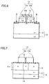
- a thermal treatment is carried out at a temperature of 1150 ⁇ for 180 minutes, whereby the n type impurities and the p type impurities are diffused.
- channel regions 4 are formed in portions of a surface of the epitaxial layer 2 disposed on both sides of the gate electrode 13, and an n type impurity region 14 is formed below the separation hole 12.
- the n type impurities implanted from the separation hole 12 are diffused in a vertical direction with respect to the depth of the substrate, and simultaneously are diffused in a lateral (horizontal) direction with respect to the substrate.
- the gate length Lg of the separated gate electrode 13a is set to be equal to or less than the depth X ch of the channel region 4
- side surfaces of the n type impurity region 14 form junction surfaces substantially parallel to the side surfaces of the channel regions 4 adjacent thereto.
- a bottom of the n type impurity region 14 and bottoms of the channel regions 4 are located at depths substantially equal to each other by the diffusion of the impurities under the conditions of the fourth step.
- the impurity concentration of the n type impurity region 14 can be improved to be higher than that in the related arts.
- the diffusion process is further carried out.
- the width of the n type impurity region 14 varies, there is no problem as long as the width thereof is within a range where the MOSFET can pinch off at the application of V DSS .
- a mask exposing a part of the channel region4 is formed by a new photoresist film PR, n + type impurities, for example, arsenic (As), are ion-implanted.
- An acceleration energy is set to 100 KeV, and a dose amount is set to about 5 ⁇ 10 15 cm -2 (see Fig. 8A).
- an insulating film 16' such as PSG (Phosphorus Silicate Glass) serving as an interlayer insulating film is deposited by a CVD method.
- the n + type impurities are diffused by a thermal treatment at the time when the insulating film 16' is formed, thus forming a source region 15 (see Fig. 8A).
- the thermal treatment is carried out at a temperature lower than 1000 ⁇ for about 60 minutes.
- a sixth step (Fig. 9):
- the insulating film 16' is etched by use of a new photoresist film (not shown) as a mask, and an interlayer insulating film 16 is left, and simultaneously contact holes CH are formed.
- the separated gate electrodes 13a and 13b above the n type impurity region 14 are wholly covered with the interlayer insulating film 16.
- a barrier metal (not shown) is formed on the entire surface of the resultant structure, and aluminum alloy is sputtered so as to have a film thickness ranging from about 20000 ⁇ to 50000 ⁇ . An alloying and thermal treatment is performed, thus forming a source electrode 18 patterned to a desired pattern. Thus, a final structure shown in Fig. 1A is obtained.
- n channel type MOSFET was described as the example in this embodiment of the present invention, and a p channel type MOSFET having an opposite conductive type to the n channel type MOSFET can be similarly embodied.
- Preferred embodiments of the present invention are not limited to these. Specifically, preferred embodiments of the present invention can be similarly embodied and the same effects can be achieved as long as the semiconductor element is one of insulated gate type including an IGBT (Insulated Gate Bipolar Transistor) which is an insulated gate type bipolar transistor and in which a semiconductor layer having an opposite conductivity type to the one conductivity type semiconductor substrate 1 is disposed below the substrate 1.
- IGBT Insulated Gate Bipolar Transistor
- the n type impurity region is provided, whereby the junction surface in which the side surface of the channel region is substantially perpendicular to the side surface of the n type impurity region can be formed. Accordingly, a width of an interval between the channel regions is constant from the surface of the channel regions to the bottom thereof. Then, by forming the n type impurity region under the condition that the depletion layer extending from both sides of the channel regions is pinched off (with a certain impurity concentration and a certain width), the pinch-off of the depletion layer is sufficient even in the bottom portion of the channel region. Thus, it is possible to avoid a breakdown in corner portions of the channel regions (regions "a" of Fig. 10).
- the diffusion step of forming the channel region by setting the depth X ch of the channel region to be not less than the gate length Lg of the separated gate electrodes of one cell, it is possible to provide the n type impurity region having the junction surface perpendicular to the side surface of the channel region and having the depth equal to that of the channel region.
- the separation width L KT of the separated gate electrodes: the depth X ch of the channel region, which is equal to or less than 0.6 : 4) it is possible to form the n type impurity region forming the junction surface perpendicular to the channel region, and it is possible to make the width of the n type impurity region equal to the width having a value for pinching off the depletion layer in the n type impurity region.
- the drain-to-source voltage V DSS of not less than 600 V can be obtained.
- the depletion layer is fully pinched off even in the vicinity of the bottom portion of the channel region, it is possible to increase the impurity concentration of the n type impurity region up to 1 ⁇ 10 17 cm -3 . Hence, it is possible to achieve a low resistance in the ON state of the MOSFET and an increase of the breakdown voltage in the OFF state thereof.
- the n type impurity region is formed in the diffusion step for forming the channel region.
- a control of the depth of the n type impurity region is made easier without being influenced by the thermal treatment during the formation of the gate electrode.
- the bottoms thereof are substantially uniform.
- boron is implanted into the channel region under the condition that the acceleration energy is 80 KeV and the dose amount is 2 ⁇ 10 13 cm -2
- phosphor is implanted into the n type impurity region under condition that the acceleration energy is 120 KeV and the dose amount is 1 ⁇ 10 13 cm -2
- the thermal treatment is carried out at the temperature of 1150 D.
- the channel region and the n type impurity region have the substantially uniform depth.
- the n type impurity region has an impurity concentration, which is about 1 ⁇ 10 17 cm -3 and is higher than that in the related art, the depletion layer is pinched off vertically in the depth direction of the substrate.
- the predetermined breakdown voltage is obtained.
- the drain-to-source breakdown voltage of not less than 600 V can be obtained.
Landscapes
- Insulated Gate Type Field-Effect Transistor (AREA)
- Junction Field-Effect Transistors (AREA)
Applications Claiming Priority (1)
| Application Number | Priority Date | Filing Date | Title |
|---|---|---|---|
| JP2005077570 | 2005-03-17 |
Publications (2)
| Publication Number | Publication Date |
|---|---|
| EP1703567A2 true EP1703567A2 (de) | 2006-09-20 |
| EP1703567A3 EP1703567A3 (de) | 2008-07-02 |
Family
ID=36589356
Family Applications (1)
| Application Number | Title | Priority Date | Filing Date |
|---|---|---|---|
| EP06005521A Withdrawn EP1703567A3 (de) | 2005-03-17 | 2006-03-17 | Feldeffekttransistor mit isoliertem Gate und Verfahren zu dessen Herstellung |
Country Status (3)
| Country | Link |
|---|---|
| EP (1) | EP1703567A3 (de) |
| CN (1) | CN100536166C (de) |
| TW (1) | TWI289356B (de) |
Cited By (1)
| Publication number | Priority date | Publication date | Assignee | Title |
|---|---|---|---|---|
| CN117352539A (zh) * | 2023-10-10 | 2024-01-05 | 汇能微电子技术(深圳)有限公司 | 半导体器件结构及其制备方法 |
Families Citing this family (1)
| Publication number | Priority date | Publication date | Assignee | Title |
|---|---|---|---|---|
| CN102737990A (zh) * | 2011-04-12 | 2012-10-17 | 北大方正集团有限公司 | 处理半导体器件的方法、装置和系统 |
Citations (1)
| Publication number | Priority date | Publication date | Assignee | Title |
|---|---|---|---|---|
| JPH10335643A (ja) * | 1997-06-05 | 1998-12-18 | Toshiba Corp | 半導体装置の製造方法 |
Family Cites Families (4)
| Publication number | Priority date | Publication date | Assignee | Title |
|---|---|---|---|---|
| JP3448138B2 (ja) * | 1995-10-05 | 2003-09-16 | 株式会社日立製作所 | 半導体装置の製造方法 |
| DE19902749C2 (de) * | 1999-01-25 | 2002-02-07 | Infineon Technologies Ag | Leistungstransistoranordnung mit hoher Spannungsfestigkeit |
| JP2001119025A (ja) * | 1999-10-21 | 2001-04-27 | Matsushita Electric Ind Co Ltd | 半導体素子およびその形成方法 |
| JP3906105B2 (ja) * | 2002-03-29 | 2007-04-18 | 株式会社東芝 | 半導体装置 |
-
2006
- 2006-01-04 TW TW095100268A patent/TWI289356B/zh not_active IP Right Cessation
- 2006-01-28 CN CNB2006100042014A patent/CN100536166C/zh not_active Expired - Fee Related
- 2006-03-17 EP EP06005521A patent/EP1703567A3/de not_active Withdrawn
Patent Citations (1)
| Publication number | Priority date | Publication date | Assignee | Title |
|---|---|---|---|---|
| JPH10335643A (ja) * | 1997-06-05 | 1998-12-18 | Toshiba Corp | 半導体装置の製造方法 |
Cited By (1)
| Publication number | Priority date | Publication date | Assignee | Title |
|---|---|---|---|---|
| CN117352539A (zh) * | 2023-10-10 | 2024-01-05 | 汇能微电子技术(深圳)有限公司 | 半导体器件结构及其制备方法 |
Also Published As
| Publication number | Publication date |
|---|---|
| CN100536166C (zh) | 2009-09-02 |
| CN1835249A (zh) | 2006-09-20 |
| EP1703567A3 (de) | 2008-07-02 |
| TW200635043A (en) | 2006-10-01 |
| TWI289356B (en) | 2007-11-01 |
Similar Documents
| Publication | Publication Date | Title |
|---|---|---|
| US7858478B2 (en) | Method for producing an integrated circuit including a trench transistor and integrated circuit | |
| US6518128B2 (en) | Trench MOSFET with double-diffused body profile | |
| US8133788B2 (en) | Method of manufacturing semiconductor device | |
| US20090085111A1 (en) | Semiconductor device and method of manufacturing the same | |
| KR101293927B1 (ko) | 스크리닝 전극을 가진 반도체 장치 및 방법 | |
| KR101332590B1 (ko) | 개선된 성능을 갖는 파워 반도체 장치 및 방법 | |
| US10069006B2 (en) | Semiconductor device with vertical field floating rings and methods of fabrication thereof | |
| JP2005510088A (ja) | 多結晶シリコンソースコンタクト構造を有するトレンチ金属酸化膜半導体電界効果トランジスタデバイス | |
| JP2010021176A (ja) | 半導体装置および半導体装置の製造方法 | |
| JPH11163341A (ja) | 炭化珪素半導体装置 | |
| JP2005520319A (ja) | 対称的トレンチ金属酸化膜半導体電界効果トランジスタ素子及びその製造方法 | |
| WO2015174197A1 (ja) | 半導体装置および半導体装置の製造方法 | |
| JP2005536868A (ja) | 寄生抵抗が低いトレンチ金属酸化膜半導体電界効果トランジスタデバイスの製造方法 | |
| JP4440188B2 (ja) | 半導体装置の製造方法 | |
| JP2007087985A (ja) | 絶縁ゲート型半導体装置およびその製造方法 | |
| US20050112823A1 (en) | Trench power MOSFET with reduced gate resistance | |
| US7514332B2 (en) | Semiconductor device and method for manufacturing the same | |
| US7723784B2 (en) | Insulated gate semiconductor device and method for manufacturing the same | |
| EP1703567A2 (de) | Feldeffekttransistor mit isoliertem Gate und Verfahren zu dessen Herstellung | |
| JP2005026391A (ja) | Mos型半導体装置 | |
| JP4992211B2 (ja) | 半導体素子の製造方法 | |
| US20080054348A1 (en) | Semiconductor device and a method of fabricating the same | |
| JP5037103B2 (ja) | 炭化珪素半導体装置 | |
| US6878997B2 (en) | Compensation component and method for fabricating the component | |
| JPH09260659A (ja) | 半導体素子およびその製造方法 |
Legal Events
| Date | Code | Title | Description |
|---|---|---|---|
| PUAI | Public reference made under article 153(3) epc to a published international application that has entered the european phase |
Free format text: ORIGINAL CODE: 0009012 |
|
| AK | Designated contracting states |
Kind code of ref document: A2 Designated state(s): AT BE BG CH CY CZ DE DK EE ES FI FR GB GR HU IE IS IT LI LT LU LV MC NL PL PT RO SE SI SK TR |
|
| AX | Request for extension of the european patent |
Extension state: AL BA HR MK YU |
|
| PUAL | Search report despatched |
Free format text: ORIGINAL CODE: 0009013 |
|
| AK | Designated contracting states |
Kind code of ref document: A3 Designated state(s): AT BE BG CH CY CZ DE DK EE ES FI FR GB GR HU IE IS IT LI LT LU LV MC NL PL PT RO SE SI SK TR |
|
| AX | Request for extension of the european patent |
Extension state: AL BA HR MK YU |
|
| RIC1 | Information provided on ipc code assigned before grant |
Ipc: H01L 29/739 20060101ALN20080528BHEP Ipc: H01L 29/08 20060101ALI20080528BHEP Ipc: H01L 29/423 20060101ALI20080528BHEP Ipc: H01L 21/336 20060101ALI20080528BHEP Ipc: H01L 29/78 20060101AFI20060627BHEP |
|
| 17P | Request for examination filed |
Effective date: 20080918 |
|
| 17Q | First examination report despatched |
Effective date: 20081021 |
|
| AKX | Designation fees paid |
Designated state(s): DE |
|
| STAA | Information on the status of an ep patent application or granted ep patent |
Free format text: STATUS: THE APPLICATION IS DEEMED TO BE WITHDRAWN |
|
| 18D | Application deemed to be withdrawn |
Effective date: 20141001 |