EP1699082A1 - Solid-state image sensing device - Google Patents
Solid-state image sensing device Download PDFInfo
- Publication number
- EP1699082A1 EP1699082A1 EP06251097A EP06251097A EP1699082A1 EP 1699082 A1 EP1699082 A1 EP 1699082A1 EP 06251097 A EP06251097 A EP 06251097A EP 06251097 A EP06251097 A EP 06251097A EP 1699082 A1 EP1699082 A1 EP 1699082A1
- Authority
- EP
- European Patent Office
- Prior art keywords
- image sensing
- solid
- state image
- printed board
- bore
- Prior art date
- Legal status (The legal status is an assumption and is not a legal conclusion. Google has not performed a legal analysis and makes no representation as to the accuracy of the status listed.)
- Withdrawn
Links
Images




Classifications
-
- H—ELECTRICITY
- H10—SEMICONDUCTOR DEVICES; ELECTRIC SOLID-STATE DEVICES NOT OTHERWISE PROVIDED FOR
- H10F—INORGANIC SEMICONDUCTOR DEVICES SENSITIVE TO INFRARED RADIATION, LIGHT, ELECTROMAGNETIC RADIATION OF SHORTER WAVELENGTH OR CORPUSCULAR RADIATION
- H10F39/00—Integrated devices, or assemblies of multiple devices, comprising at least one element covered by group H10F30/00, e.g. radiation detectors comprising photodiode arrays
- H10F39/10—Integrated devices
- H10F39/12—Image sensors
-
- H—ELECTRICITY
- H10—SEMICONDUCTOR DEVICES; ELECTRIC SOLID-STATE DEVICES NOT OTHERWISE PROVIDED FOR
- H10F—INORGANIC SEMICONDUCTOR DEVICES SENSITIVE TO INFRARED RADIATION, LIGHT, ELECTROMAGNETIC RADIATION OF SHORTER WAVELENGTH OR CORPUSCULAR RADIATION
- H10F77/00—Constructional details of devices covered by this subclass
- H10F77/50—Encapsulations or containers
-
- H—ELECTRICITY
- H10—SEMICONDUCTOR DEVICES; ELECTRIC SOLID-STATE DEVICES NOT OTHERWISE PROVIDED FOR
- H10F—INORGANIC SEMICONDUCTOR DEVICES SENSITIVE TO INFRARED RADIATION, LIGHT, ELECTROMAGNETIC RADIATION OF SHORTER WAVELENGTH OR CORPUSCULAR RADIATION
- H10F39/00—Integrated devices, or assemblies of multiple devices, comprising at least one element covered by group H10F30/00, e.g. radiation detectors comprising photodiode arrays
- H10F39/80—Constructional details of image sensors
- H10F39/804—Containers or encapsulations
-
- H—ELECTRICITY
- H10—SEMICONDUCTOR DEVICES; ELECTRIC SOLID-STATE DEVICES NOT OTHERWISE PROVIDED FOR
- H10W—GENERIC PACKAGES, INTERCONNECTIONS, CONNECTORS OR OTHER CONSTRUCTIONAL DETAILS OF DEVICES COVERED BY CLASS H10
- H10W72/00—Interconnections or connectors in packages
- H10W72/071—Connecting or disconnecting
- H10W72/072—Connecting or disconnecting of bump connectors
- H10W72/07251—Connecting or disconnecting of bump connectors characterised by changes in properties of the bump connectors during connecting
-
- H—ELECTRICITY
- H10—SEMICONDUCTOR DEVICES; ELECTRIC SOLID-STATE DEVICES NOT OTHERWISE PROVIDED FOR
- H10W—GENERIC PACKAGES, INTERCONNECTIONS, CONNECTORS OR OTHER CONSTRUCTIONAL DETAILS OF DEVICES COVERED BY CLASS H10
- H10W72/00—Interconnections or connectors in packages
- H10W72/20—Bump connectors, e.g. solder bumps or copper pillars; Dummy bumps; Thermal bumps
-
- H—ELECTRICITY
- H10—SEMICONDUCTOR DEVICES; ELECTRIC SOLID-STATE DEVICES NOT OTHERWISE PROVIDED FOR
- H10W—GENERIC PACKAGES, INTERCONNECTIONS, CONNECTORS OR OTHER CONSTRUCTIONAL DETAILS OF DEVICES COVERED BY CLASS H10
- H10W72/00—Interconnections or connectors in packages
- H10W72/90—Bond pads, in general
-
- H—ELECTRICITY
- H10—SEMICONDUCTOR DEVICES; ELECTRIC SOLID-STATE DEVICES NOT OTHERWISE PROVIDED FOR
- H10W—GENERIC PACKAGES, INTERCONNECTIONS, CONNECTORS OR OTHER CONSTRUCTIONAL DETAILS OF DEVICES COVERED BY CLASS H10
- H10W72/00—Interconnections or connectors in packages
- H10W72/90—Bond pads, in general
- H10W72/921—Structures or relative sizes of bond pads
- H10W72/923—Bond pads having multiple stacked layers
-
- H—ELECTRICITY
- H10—SEMICONDUCTOR DEVICES; ELECTRIC SOLID-STATE DEVICES NOT OTHERWISE PROVIDED FOR
- H10W—GENERIC PACKAGES, INTERCONNECTIONS, CONNECTORS OR OTHER CONSTRUCTIONAL DETAILS OF DEVICES COVERED BY CLASS H10
- H10W72/00—Interconnections or connectors in packages
- H10W72/90—Bond pads, in general
- H10W72/941—Dispositions of bond pads
- H10W72/9415—Dispositions of bond pads relative to the surface, e.g. recessed, protruding
-
- H—ELECTRICITY
- H10—SEMICONDUCTOR DEVICES; ELECTRIC SOLID-STATE DEVICES NOT OTHERWISE PROVIDED FOR
- H10W—GENERIC PACKAGES, INTERCONNECTIONS, CONNECTORS OR OTHER CONSTRUCTIONAL DETAILS OF DEVICES COVERED BY CLASS H10
- H10W72/00—Interconnections or connectors in packages
- H10W72/90—Bond pads, in general
- H10W72/941—Dispositions of bond pads
- H10W72/942—Dispositions of bond pads relative to underlying supporting features, e.g. bond pads, RDLs or vias
Definitions
- the present invention relates to a solid-state image sensing device suitable as a component of an optical device module.
- a solid-state image sensing element such as a CCD or a CMOS image sensor
- a light-transmitting lid section that covers the image sensing area of the solid-state image sensing element is fixed to the solid-state image sensing element through an adhesive layer.
- a plurality of connecting terminals of the printed board are connected to a plurality of connecting terminals of the solid-state image sensing element by wires.
- the present invention has been made with the aim of solving the above problem, and it is an object of the present invention to provide a solid-state image sensing device which is made thinner than the conventional one by providing a bore in a printed board and allowing at least a part of a light-transmitting lid section to be fitted in the bore.
- Another object of the present invention is to provide a solid-state image sensing device in which at least a part of a solid-state image sensing element is fitted in a bore of a printed board, whereby the protective function of the solid-state image sensing element is enhanced by the printed board.
- Still another object of the present invention is to provide a solid-state image sensing device, the strength of which is increased by a sealing material.
- Another object of the present invention is to provide a solid-state image sensing device in which at least a part of another electronic component is fitted in a bore, whereby the protective function of the electronic component is enhanced by a printed board.
- Still another object of the present invention is to provide a solid-state image sensing device including an electronic component, the strength of which is increased by a sealing material.
- the present invention employs the following means.
- a solid-state image sensing device is a solid-state image sensing device, comprising: a printed board; a solid-state image sensing element fixed to the printed board; and a light-transmitting lid section fixed to the solid-state image sensing element so as to cover an image sensing area, wherein the printed board has a bore which penetrates through the printed board in a thickness direction thereof, at least a part of the light-transmitting lid section is fitted in the bore, and a connecting terminal of the printed board is connected to a connecting terminal of the solid-state image sensing element.
- the solid-state image sensing device is characterized in that at an inner surface of the bore is formed a flat surface which is parallel to one side of the printed board and on which the connecting terminal of the printed board is provided, and the solid-state image sensing element is fixed to the flat surface.
- the solid-state image sensing device is characterized in that a sealing material is filled in space provided between side surfaces of the solid-state image sensing element and the light-transmitting lid section, and the inner surface of the bore.
- the solid-state image sensing device is characterized in that at an inner surface of the bore are formed two step-like flat surfaces which are parallel to one side of the printed board and on which connecting terminals of the printed board are provided respectively, the solid-state image sensing element is fixed to one of the flat surfaces that is further away from the one side, an electronic component is fixed to the other of the flat surfaces that is closer to the one side, and a connecting terminal of the electronic component is connected to the connecting terminal of the printed board.
- the solid-state image sensing device is characterized in that a sealing material is filled in space provided between side surfaces of the electronic component and the light-transmitting lid section, and the inner surface of the bore.
- a solid-state image sensing device thinner than the conventional one can be obtained.
- a connecting terminal of the printed board is connected to a connecting terminal of a solid-state image sensing element, a problem associated with a connection by wire bonding can be overcome.
- the solid-state image sensing element since at least a part of a solid-state image sensing element is fitted in a bore, the solid-state image sensing element can be protected by a printed board.
- the overall strength of a solid-state image sensing device can be increased by a sealing material.
- the electronic component since at least a part of an electronic component is fitted in a bore, the electronic component can be protected by a printed board.
- the overall strength of a solid-state image sensing device including an electronic component can be increased by a sealing material.
- FIG. 1 is a schematic vertical end view showing a first embodiment of the present invention
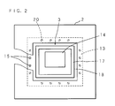
- FIG. 2 is a view when viewed from line II-II of FIG. 1
- FIG. 3 is a view when viewed from line III-III of FIG. 1.
- a bore 3 which is rectangular when viewed from the top is provided in the center of a printed board 2 which is rectangular when viewed from the top and which is provided with conductive wirings (not shown), so as to penetrate through the printed board 2 in a thickness direction thereof.
- a step portion 7 having a flat surface 6 parallel to an under surface of the printed board 2.
- the form of the bore 3 when viewed from the top is in a size into which a light-transmitting lid section 17 fits.
- the form of the bore 3 when viewed from the bottom is in a size into which a solid-state image sensing element 13 fits.
- a plurality of connecting terminals 9 are provided on the flat surface 6 with appropriate spacing therebetween.
- a plurality of connecting terminals 10 for establishing a connection to an external device are provided on the under surface of the printed board 2 with appropriate spacing therebetween.
- the connecting terminals 9 and 10 are connected to their corresponding conductive wirings on the printed board 2.
- the connecting terminals 9 on the flat surface 6 of the printed board 2 are respectively connected, via bumps 20, to connecting terminals 15 provided on a periphery of a top side of the solid-state image sensing element 13 and opposed to the connecting terminals 9, by flip-chip bonding.
- the solid-state image sensing element 13 is fixed to the flat surface 6.
- Examples of the solid-state image sensing element 13 include a CCD and a CMOS image sensor. Although the entire solid-state image sensing element 13 is fitted in the bore 3, only a part of the solid-state image sensing element 13 may be fitted in the bore 3.
- the solid-state image sensing element 13 is rectangular when viewed from the top.
- An image sensing area (effective pixel area) 14 which is rectangular when viewed from the top faces upward.
- the light-transmitting lid section 17 which is rectangular when viewed from the top covers the image sensing area 14 to protect the image sensing area 14 from dust, and has an optical filter function.
- the light-transmitting lid section 17 is fixed to the solid-state image sensing element 13 through an adhesive layer 18 provided on the top side of the solid-state image sensing element 13.
- the form of the light-transmitting lid section 17 when viewed from the top is greater than that of the image sensing area 14.
- the adhesive layer 18 is provided all around the periphery of the light-transmitting lid section 17. Although the entire light-transmitting lid section 17 is fitted in the bore 3, only a part of the light-transmitting lid section 17 may be fitted in the bore 3.
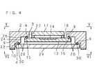
- FIG. 4 is a schematic vertical end view showing a second embodiment of the present invention
- FIG. 5 is a view when viewed from line V-V of FIG. 4
- FIG. 6 is a view when viewed from line VI-VI of FIG. 4.
- a first step portion 24 having a first flat surface 23 which is parallel to an under surface of the printed board 2 and on which connecting terminals 9 of the printed board 2 is provided.
- a second step portion 27 having a second flat surface 26 which is parallel to the under surface of the printed board 2 and on which connecting terminals 9 of the printed board 2 is provided, such that the second step portion 27 is located above the first step portion 24.
- a solid-state image sensing element 13 is opposed to the second flat surface 26 with a light-transmitting lid section 17 facing upward.
- the connecting terminals 9 on the second flat surface 26 are respectively connected, via bumps 20, to connecting terminals 15 of the solid-state image sensing element 13 that are opposed to the connecting terminals 9, by flip-chip bonding.
- the connecting terminals 9 on the first flat surface 23 are respectively connected, via bumps 20, to connecting terminals 30 provided on a periphery of a top side of another electronic component 29 and opposed to the connecting terminals 9, by flip-chip bonding.
- the electronic component 29 is fixed to the first flat surface 23 of the printed board 2.
- Examples of the electronic component 29 include a digital signal processor, a drive circuit for a CCD, a resistor for an external filter circuit, and a capacitor.
- the electronic component 29 is rectangular when viewed from the top. Also in the present embodiment, the entire light-transmitting lid section 17 and the entire electronic component 29 are fitted in the bore 3; however, only a part of the electronic component 29 may be fitted in the bore 3.
- FIG. 7 is a schematic vertical end view showing a third embodiment of the present invention.
- a sealing material 32 made of a synthetic resin is filled in space provided between side surfaces of a solid-state image sensing element 13, an outer surface of an adhesive layer 18, and side surfaces of a light-transmitting lid section 17, and an inner surface 4 of a bore 3.
- Other components are the same as those in the first embodiment; therefore, the same components are denoted by the same reference numerals and a detailed description thereof is omitted.
- the sealing material 32 protects bumps 20 and also increases the overall strength of a solid-state image sensing device.
- FIG. 8 is a schematic vertical end view showing a fourth embodiment of the present invention.
- a sealing material 32 is filled in space provided between side surfaces of an electronic component 29 and an inner surface 4 of a bore 3.
- a sealing material 32 is filled in space provided between an outer surface of an adhesive layer 18 and side surfaces of a light-transmitting lid section 17, and the inner surface 4 of the bore 3.
- Other components are the same as those in the second embodiment; therefore, the same components are denoted by the same reference numerals and a detailed description thereof is omitted.
- the sealing material 32 protects bumps 20 and also increases the overall strength of a solid-state image sensing device.
Landscapes
- Solid State Image Pick-Up Elements (AREA)
- Transforming Light Signals Into Electric Signals (AREA)
- Studio Devices (AREA)
Abstract
A solid-state image sensing device has a printed board (2); a solid-state image sensing element (13) fixed to the printed board (2); and a light-transmitting lid section (17) fixed to the solid-state image sensing element (13) so as to cover an image sensing area (effective pixel area) (14). The printed board (2) has a bore (8) which penetrates through the printed board (2) in a thickness direction thereof, at least a part of the light-transmitting lid section (17) is fitted in the bore (3), and connecting terminals (9) of the printed board (2) are connected to connecting terminals (15) of the solid-state image sensing element (13).
Description
- The present invention relates to a solid-state image sensing device suitable as a component of an optical device module.
- As a conventional solid-state image sensing device, the one shown in Japanese Patent Application Laid Open No. 2004-296453 is known.
- Specifically, a solid-state image sensing element, such as a CCD or a CMOS image sensor, is fixed on a printed board at an opposite surface of an image sensing area, and a light-transmitting lid section that covers the image sensing area of the solid-state image sensing element is fixed to the solid-state image sensing element through an adhesive layer. A plurality of connecting terminals of the printed board are connected to a plurality of connecting terminals of the solid-state image sensing element by wires.
- There is a demand for reduction in the thickness of the conventional solid-state image sensing device.
- The present invention has been made with the aim of solving the above problem, and it is an object of the present invention to provide a solid-state image sensing device which is made thinner than the conventional one by providing a bore in a printed board and allowing at least a part of a light-transmitting lid section to be fitted in the bore.
- Another object of the present invention is to provide a solid-state image sensing device in which at least a part of a solid-state image sensing element is fitted in a bore of a printed board, whereby the protective function of the solid-state image sensing element is enhanced by the printed board.
- Still another object of the present invention is to provide a solid-state image sensing device, the strength of which is increased by a sealing material.
- Another object of the present invention is to provide a solid-state image sensing device in which at least a part of another electronic component is fitted in a bore, whereby the protective function of the electronic component is enhanced by a printed board.
- Still another object of the present invention is to provide a solid-state image sensing device including an electronic component, the strength of which is increased by a sealing material.
- To attain the above objects, the present invention employs the following means.
- A solid-state image sensing device according to the present invention is a solid-state image sensing device, comprising: a printed board; a solid-state image sensing element fixed to the printed board; and a light-transmitting lid section fixed to the solid-state image sensing element so as to cover an image sensing area, wherein the printed board has a bore which penetrates through the printed board in a thickness direction thereof, at least a part of the light-transmitting lid section is fitted in the bore, and a connecting terminal of the printed board is connected to a connecting terminal of the solid-state image sensing element.
- The solid-state image sensing device according to the present invention is characterized in that at an inner surface of the bore is formed a flat surface which is parallel to one side of the printed board and on which the connecting terminal of the printed board is provided, and the solid-state image sensing element is fixed to the flat surface.
- The solid-state image sensing device according to the present invention is characterized in that a sealing material is filled in space provided between side surfaces of the solid-state image sensing element and the light-transmitting lid section, and the inner surface of the bore.
- The solid-state image sensing device according to the present invention is characterized in that at an inner surface of the bore are formed two step-like flat surfaces which are parallel to one side of the printed board and on which connecting terminals of the printed board are provided respectively, the solid-state image sensing element is fixed to one of the flat surfaces that is further away from the one side, an electronic component is fixed to the other of the flat surfaces that is closer to the one side, and a connecting terminal of the electronic component is connected to the connecting terminal of the printed board.
- The solid-state image sensing device according to the present invention is characterized in that a sealing material is filled in space provided between side surfaces of the electronic component and the light-transmitting lid section, and the inner surface of the bore.
- According to the present invention, since at least a part of a light-transmitting lid section is fitted in a bore of a printed board, a solid-state image sensing device thinner than the conventional one can be obtained. In addition, since a connecting terminal of the printed board is connected to a connecting terminal of a solid-state image sensing element, a problem associated with a connection by wire bonding can be overcome.
- According to the present invention, since at least a part of a solid-state image sensing element is fitted in a bore, the solid-state image sensing element can be protected by a printed board.
- According to the present invention, the overall strength of a solid-state image sensing device can be increased by a sealing material.
- According to the present invention, since at least a part of an electronic component is fitted in a bore, the electronic component can be protected by a printed board.
- According to the present invention, the overall strength of a solid-state image sensing device including an electronic component can be increased by a sealing material.
- The above and further objects and features of the invention will more fully be apparent from the following detailed description with accompanying drawings.
-
- FIG. 1 is a schematic vertical end view showing a first embodiment of the present invention;
- FIG. 2 is a view when viewed from line II-II of FIG. 1;
- FIG. 3 is a view when viewed from line III-III of FIG. 1;
- FIG. 4 is a schematic vertical end view showing a second embodiment of the present invention; FIG. 5 is a view when viewed from line V-V of FIG. 4;
- FIG. 6 is a view when viewed from line VI-VI of FIG. 4;
- FIG. 7 is a schematic vertical end view showing a third embodiment of the present invention; and
- FIG. 8 is a schematic vertical end view showing a fourth embodiment of the present invention.
- Embodiments of the present invention will be explained below. The terms "above", "up", and "top" and "under" used in the explanation represent the top and bottom of the drawings.
- FIG. 1 is a schematic vertical end view showing a first embodiment of the present invention, FIG. 2 is a view when viewed from line II-II of FIG. 1, and FIG. 3 is a view when viewed from line III-III of FIG. 1. As shown in FIGS. 1 and 2, a
bore 3 which is rectangular when viewed from the top is provided in the center of a printedboard 2 which is rectangular when viewed from the top and which is provided with conductive wirings (not shown), so as to penetrate through the printedboard 2 in a thickness direction thereof. At aninner surface 4 of thebore 3 is formed astep portion 7 having aflat surface 6 parallel to an under surface of the printedboard 2. The form of thebore 3 when viewed from the top is in a size into which a light-transmittinglid section 17 fits. The form of thebore 3 when viewed from the bottom is in a size into which a solid-state image sensingelement 13 fits. As shown in FIG. 3, a plurality of connectingterminals 9 are provided on theflat surface 6 with appropriate spacing therebetween. In addition, a plurality of connectingterminals 10 for establishing a connection to an external device are provided on the under surface of the printedboard 2 with appropriate spacing therebetween. The connectingterminals board 2. - The connecting
terminals 9 on theflat surface 6 of the printedboard 2 are respectively connected, viabumps 20, to connectingterminals 15 provided on a periphery of a top side of the solid-stateimage sensing element 13 and opposed to theconnecting terminals 9, by flip-chip bonding. By such a configuration, the solid-stateimage sensing element 13 is fixed to theflat surface 6. Examples of the solid-stateimage sensing element 13 include a CCD and a CMOS image sensor. Although the entire solid-stateimage sensing element 13 is fitted in thebore 3, only a part of the solid-stateimage sensing element 13 may be fitted in thebore 3. The solid-stateimage sensing element 13 is rectangular when viewed from the top. An image sensing area (effective pixel area) 14 which is rectangular when viewed from the top faces upward. The light-transmittinglid section 17 which is rectangular when viewed from the top covers theimage sensing area 14 to protect theimage sensing area 14 from dust, and has an optical filter function. The light-transmittinglid section 17 is fixed to the solid-stateimage sensing element 13 through anadhesive layer 18 provided on the top side of the solid-stateimage sensing element 13. The form of the light-transmittinglid section 17 when viewed from the top is greater than that of theimage sensing area 14. Theadhesive layer 18 is provided all around the periphery of the light-transmittinglid section 17. Although the entire light-transmittinglid section 17 is fitted in thebore 3, only a part of the light-transmittinglid section 17 may be fitted in thebore 3. - FIG. 4 is a schematic vertical end view showing a second embodiment of the present invention, FIG. 5 is a view when viewed from line V-V of FIG. 4, and FIG. 6 is a view when viewed from line VI-VI of FIG. 4. As shown in FIGS. 4 to 6, at an
inner surface 4 of abore 3 of a printedboard 2 is formed afirst step portion 24 having a firstflat surface 23 which is parallel to an under surface of the printedboard 2 and on which connectingterminals 9 of the printedboard 2 is provided. In addition, at theinner surface 4 is formed asecond step portion 27 having a secondflat surface 26 which is parallel to the under surface of the printedboard 2 and on which connectingterminals 9 of the printedboard 2 is provided, such that thesecond step portion 27 is located above thefirst step portion 24. - A solid-state
image sensing element 13 is opposed to the secondflat surface 26 with a light-transmittinglid section 17 facing upward. The connectingterminals 9 on the secondflat surface 26 are respectively connected, viabumps 20, to connectingterminals 15 of the solid-stateimage sensing element 13 that are opposed to the connectingterminals 9, by flip-chip bonding. - The connecting
terminals 9 on the firstflat surface 23 are respectively connected, viabumps 20, to connectingterminals 30 provided on a periphery of a top side of anotherelectronic component 29 and opposed to the connectingterminals 9, by flip-chip bonding. By such a configuration, theelectronic component 29 is fixed to the firstflat surface 23 of the printedboard 2. Examples of theelectronic component 29 include a digital signal processor, a drive circuit for a CCD, a resistor for an external filter circuit, and a capacitor. Theelectronic component 29 is rectangular when viewed from the top. Also in the present embodiment, the entire light-transmittinglid section 17 and the entireelectronic component 29 are fitted in thebore 3; however, only a part of theelectronic component 29 may be fitted in thebore 3. - FIG. 7 is a schematic vertical end view showing a third embodiment of the present invention. As shown in FIG. 7, a sealing
material 32 made of a synthetic resin is filled in space provided between side surfaces of a solid-stateimage sensing element 13, an outer surface of anadhesive layer 18, and side surfaces of a light-transmittinglid section 17, and aninner surface 4 of abore 3. Other components are the same as those in the first embodiment; therefore, the same components are denoted by the same reference numerals and a detailed description thereof is omitted. The sealingmaterial 32 protectsbumps 20 and also increases the overall strength of a solid-state image sensing device. - FIG. 8 is a schematic vertical end view showing a fourth embodiment of the present invention. As shown in FIG. 8, a sealing
material 32 is filled in space provided between side surfaces of anelectronic component 29 and aninner surface 4 of abore 3. In addition, a sealingmaterial 32 is filled in space provided between an outer surface of anadhesive layer 18 and side surfaces of a light-transmittinglid section 17, and theinner surface 4 of thebore 3. Other components are the same as those in the second embodiment; therefore, the same components are denoted by the same reference numerals and a detailed description thereof is omitted. The sealingmaterial 32 protectsbumps 20 and also increases the overall strength of a solid-state image sensing device.
Claims (5)
- A solid-state image sensing device, comprising: a printed board (2); a solid-state image sensing element (13) fixed to the printed board (2); and a light-transmitting lid section (17) fixed to the solid-state image sensing element (13) so as to cover an image sensing area (14), characterized in that
the printed board (2) has a bore (3) which penetrates through the printed board (2) in a thickness direction thereof, at least a part of the light-transmitting lid section (17) is fitted in the bore (3), and a connecting terminal (9) of the printed board (2) is connected to a connecting terminal (15) of the solid-state image sensing element (13). - The solid-state image sensing device according to claim 1, wherein at an inner surface (4) of the bore (3) is formed a flat surface (6) which is parallel to one side of the printed board (2) and on which the connecting terminal (9) of the printed board (2) is provided, and the solid-state image sensing element (13) is fixed to the flat surface (6).
- The solid-state image sensing device according to claim 2, wherein a sealing material (32) is filled in space provided between side surfaces of the solid-state image sensing element (13) and the light-transmitting lid section (17), and the inner surface (4) of the bore (3).
- The solid-state image sensing device according to claim 1, wherein at an inner surface (4) of the bore (3) are formed two step-like flat surfaces (23,26) which are parallel to one side of the printed board (2) and on which connecting terminals (9) of the printed board (2) are provided respectively, the solid-state image sensing element (13) is fixed to one (26) of the flat surfaces (23,26) that is further away from the one side, an electronic component (29) is fixed to the other (23) of the flat surfaces (23,26) that is closer to the one side, and a connecting terminal (30) of the electronic component (29) is connected to the connecting terminal (9) of the printed board (2).
- The solid-state image sensing device according to claim 4, wherein a sealing material (32) is filled in space provided between side surfaces of the electronic component (29) and the light-transmitting lid section (17), and the inner surface (4) of the bore (3).
Applications Claiming Priority (1)
| Application Number | Priority Date | Filing Date | Title |
|---|---|---|---|
| JP2005058128A JP2006245246A (en) | 2005-03-02 | 2005-03-02 | Solid-state imaging device |
Publications (1)
| Publication Number | Publication Date |
|---|---|
| EP1699082A1 true EP1699082A1 (en) | 2006-09-06 |
Family
ID=36607464
Family Applications (1)
| Application Number | Title | Priority Date | Filing Date |
|---|---|---|---|
| EP06251097A Withdrawn EP1699082A1 (en) | 2005-03-02 | 2006-03-01 | Solid-state image sensing device |
Country Status (6)
| Country | Link |
|---|---|
| US (1) | US20060208182A1 (en) |
| EP (1) | EP1699082A1 (en) |
| JP (1) | JP2006245246A (en) |
| KR (1) | KR100808962B1 (en) |
| CN (1) | CN1828920A (en) |
| TW (1) | TWI302742B (en) |
Cited By (2)
| Publication number | Priority date | Publication date | Assignee | Title |
|---|---|---|---|---|
| EP2506302A4 (en) * | 2009-11-26 | 2013-11-06 | Kyocera Corp | WIRING SUBSTRATE, IMAGING DEVICE, AND IMAGING DEVICE MODULE |
| US11877044B2 (en) | 2016-02-18 | 2024-01-16 | Ningbo Sunny Opotech Co., Ltd. | Integral packaging process-based camera module, integral base component of same, and manufacturing method thereof |
Families Citing this family (15)
| Publication number | Priority date | Publication date | Assignee | Title |
|---|---|---|---|---|
| KR100824997B1 (en) | 2006-11-24 | 2008-04-24 | 테라셈 주식회사 | Manufacturing Method of Semiconductor Chip Package for Image Sensor |
| DE102007007503A1 (en) * | 2007-02-15 | 2008-08-21 | Robert Bosch Gmbh | component assembly |
| US7663095B2 (en) * | 2007-09-20 | 2010-02-16 | Avago Technologies Ecbu Ip (Singapore) Pte. Ltd. | Photodetector with embedded infrared filter |
| JP4443600B2 (en) | 2007-12-03 | 2010-03-31 | シャープ株式会社 | Method for manufacturing solid-state imaging device |
| JP2009239898A (en) * | 2008-03-06 | 2009-10-15 | Nec Electronics Corp | Solid-state image sensor and package for the same |
| JP2010232555A (en) | 2009-03-27 | 2010-10-14 | Oki Semiconductor Co Ltd | Manufacturing method of semiconductor device |
| KR101026829B1 (en) | 2009-07-09 | 2011-04-06 | 엘지이노텍 주식회사 | Camera module and its manufacturing method |
| JP2011210808A (en) * | 2010-03-29 | 2011-10-20 | Casio Computer Co Ltd | Semiconductor structure and semiconductor device |
| JP5601081B2 (en) * | 2010-08-11 | 2014-10-08 | 株式会社ニコン | Imaging element unit and imaging apparatus |
| KR101779498B1 (en) * | 2010-11-16 | 2017-09-18 | 엘지이노텍 주식회사 | Camera module |
| EP2641391B1 (en) * | 2010-11-18 | 2017-10-18 | LG Innotek Co., Ltd. | Camera module and method for manufacturing the same |
| CN103270757B (en) * | 2011-03-11 | 2015-07-22 | 富士胶片株式会社 | Imaging device and method for controlling operation thereof |
| CN105611135B (en) * | 2015-11-13 | 2019-03-19 | 宁波舜宇光电信息有限公司 | System-level camera module and its electrical bracket and manufacturing method |
| EP3376751B1 (en) * | 2015-11-13 | 2021-04-21 | Ningbo Sunny Opotech Co., Ltd. | Camera module, electrical support thereof, and assembling method therefor |
| CN107644883B (en) * | 2016-07-21 | 2019-12-31 | 许志行 | Portable electronic device and its image acquisition module |
Citations (6)
| Publication number | Priority date | Publication date | Assignee | Title |
|---|---|---|---|---|
| JP2002043451A (en) * | 2000-07-24 | 2002-02-08 | Kyocera Corp | Semiconductor device |
| US20020088987A1 (en) * | 2000-12-26 | 2002-07-11 | Kazunori Sakurai | Optical device and method for manufacturing the same, and electronic apparatus |
| US6566745B1 (en) * | 1999-03-29 | 2003-05-20 | Imec Vzw | Image sensor ball grid array package and the fabrication thereof |
| US6696738B1 (en) * | 2002-11-12 | 2004-02-24 | Kingpak Technology Inc. | Miniaturized image sensor |
| EP1445803A2 (en) * | 2003-02-06 | 2004-08-11 | Sharp Kabushiki Kaisha | Solid state imaging device with sealing window smaller than the imager chip |
| US6784534B1 (en) * | 2002-02-06 | 2004-08-31 | Amkor Technology, Inc. | Thin integrated circuit package having an optically transparent window |
Family Cites Families (9)
| Publication number | Priority date | Publication date | Assignee | Title |
|---|---|---|---|---|
| EP0790652B1 (en) * | 1995-08-02 | 2007-02-21 | Matsushita Electric Industrial Co., Ltd. | Solid-state image pickup device and its manufacture |
| JP4004705B2 (en) * | 2000-02-29 | 2007-11-07 | 松下電器産業株式会社 | Imaging device and imaging device assembling method |
| JP2001358997A (en) * | 2000-06-12 | 2001-12-26 | Mitsubishi Electric Corp | Semiconductor device |
| JP3646933B2 (en) * | 2001-11-22 | 2005-05-11 | 松下電器産業株式会社 | Solid-state imaging device and manufacturing method thereof |
| JP4184125B2 (en) * | 2002-04-26 | 2008-11-19 | 富士フイルム株式会社 | Image sensor chip module |
| US7274094B2 (en) * | 2002-08-28 | 2007-09-25 | Micron Technology, Inc. | Leadless packaging for image sensor devices |
| KR100502212B1 (en) * | 2003-01-04 | 2005-07-19 | 김영호 | Image Sensor And Manufacturing Method Thereof |
| JP4303610B2 (en) * | 2003-05-19 | 2009-07-29 | 富士フイルム株式会社 | Multilayer wiring board, component mounting method, and imaging apparatus |
| US7645635B2 (en) * | 2004-08-16 | 2010-01-12 | Micron Technology, Inc. | Frame structure and semiconductor attach process for use therewith for fabrication of image sensor packages and the like, and resulting packages |
-
2005
- 2005-03-02 JP JP2005058128A patent/JP2006245246A/en active Pending
-
2006
- 2006-03-01 EP EP06251097A patent/EP1699082A1/en not_active Withdrawn
- 2006-03-01 US US11/366,945 patent/US20060208182A1/en not_active Abandoned
- 2006-03-02 CN CNA2006100594043A patent/CN1828920A/en active Pending
- 2006-03-02 KR KR1020060020148A patent/KR100808962B1/en not_active Expired - Fee Related
- 2006-03-02 TW TW095107023A patent/TWI302742B/en not_active IP Right Cessation
Patent Citations (7)
| Publication number | Priority date | Publication date | Assignee | Title |
|---|---|---|---|---|
| US6566745B1 (en) * | 1999-03-29 | 2003-05-20 | Imec Vzw | Image sensor ball grid array package and the fabrication thereof |
| JP2002043451A (en) * | 2000-07-24 | 2002-02-08 | Kyocera Corp | Semiconductor device |
| US20020088987A1 (en) * | 2000-12-26 | 2002-07-11 | Kazunori Sakurai | Optical device and method for manufacturing the same, and electronic apparatus |
| US6784534B1 (en) * | 2002-02-06 | 2004-08-31 | Amkor Technology, Inc. | Thin integrated circuit package having an optically transparent window |
| US6696738B1 (en) * | 2002-11-12 | 2004-02-24 | Kingpak Technology Inc. | Miniaturized image sensor |
| EP1445803A2 (en) * | 2003-02-06 | 2004-08-11 | Sharp Kabushiki Kaisha | Solid state imaging device with sealing window smaller than the imager chip |
| JP2004296453A (en) | 2003-02-06 | 2004-10-21 | Sharp Corp | Solid-state imaging device, semiconductor wafer, module for optical device, method for manufacturing solid-state imaging device, and method for manufacturing module for optical device |
Non-Patent Citations (1)
| Title |
|---|
| PATENT ABSTRACTS OF JAPAN vol. 2002, no. 06 4 June 2002 (2002-06-04) * |
Cited By (3)
| Publication number | Priority date | Publication date | Assignee | Title |
|---|---|---|---|---|
| EP2506302A4 (en) * | 2009-11-26 | 2013-11-06 | Kyocera Corp | WIRING SUBSTRATE, IMAGING DEVICE, AND IMAGING DEVICE MODULE |
| US8659105B2 (en) | 2009-11-26 | 2014-02-25 | Kyocera Corporation | Wiring substrate, imaging device and imaging device module |
| US11877044B2 (en) | 2016-02-18 | 2024-01-16 | Ningbo Sunny Opotech Co., Ltd. | Integral packaging process-based camera module, integral base component of same, and manufacturing method thereof |
Also Published As
| Publication number | Publication date |
|---|---|
| KR100808962B1 (en) | 2008-03-04 |
| TWI302742B (en) | 2008-11-01 |
| US20060208182A1 (en) | 2006-09-21 |
| KR20060096339A (en) | 2006-09-11 |
| CN1828920A (en) | 2006-09-06 |
| JP2006245246A (en) | 2006-09-14 |
| TW200633198A (en) | 2006-09-16 |
Similar Documents
| Publication | Publication Date | Title |
|---|---|---|
| EP1699082A1 (en) | Solid-state image sensing device | |
| US7167376B2 (en) | Multilayer wiring board, method of mounting components, and image pick-up device | |
| US8847146B2 (en) | Image sensor package structure with casing including a vent without sealing and in communication with package material | |
| KR101579623B1 (en) | Semiconductor package for image sensor and manufacturing method thereof | |
| US7521790B2 (en) | Semiconductor device module and manufacturing method of semiconductor device module | |
| US6603107B2 (en) | Image pickup device and portable telephone | |
| US20170179182A1 (en) | Semiconductor package and method of fabricating the same | |
| US7638865B2 (en) | Sensor package | |
| JP2006237134A (en) | Solid-state imaging device | |
| US20070120213A1 (en) | Wire under dam package and method for packaging image-sensor | |
| JP2013085095A (en) | Imaging device | |
| CN101536489B (en) | Solid-state imaging device and electronic equipment | |
| KR102509276B1 (en) | Optical fingerprint recognition sensor module and electronic device using the same | |
| JP6121109B2 (en) | Imaging device | |
| CN217283093U (en) | Chip module, camera device and electronic equipment | |
| KR20080051445A (en) | Image sensor module and manufacturing method thereof and camera module including same | |
| CN110416241A (en) | Packaging structure, image acquisition module and smart phone terminal | |
| CN215420451U (en) | Chip module, camera device and electronic equipment | |
| KR101018225B1 (en) | Multilayer circuit board and camera module having same | |
| KR100691436B1 (en) | Image sensor module and camera module using same | |
| US20040089927A1 (en) | Modularized image sensor | |
| JP2007194441A (en) | Semiconductor device for image sensor and manufacturing method thereof | |
| US20070090380A1 (en) | Image sensor structure with a connector | |
| KR20250063476A (en) | Image sensor module | |
| JP2006217564A (en) | Image sensor package |
Legal Events
| Date | Code | Title | Description |
|---|---|---|---|
| PUAI | Public reference made under article 153(3) epc to a published international application that has entered the european phase |
Free format text: ORIGINAL CODE: 0009012 |
|
| AK | Designated contracting states |
Kind code of ref document: A1 Designated state(s): AT BE BG CH CY CZ DE DK EE ES FI FR GB GR HU IE IS IT LI LT LU LV MC NL PL PT RO SE SI SK TR |
|
| AX | Request for extension of the european patent |
Extension state: AL BA HR MK YU |
|
| 17P | Request for examination filed |
Effective date: 20070305 |
|
| AKX | Designation fees paid |
Designated state(s): DE FR GB |
|
| STAA | Information on the status of an ep patent application or granted ep patent |
Free format text: STATUS: THE APPLICATION HAS BEEN WITHDRAWN |
|
| 18W | Application withdrawn |
Effective date: 20081030 |