EP1445803A2 - Solid state imaging device with sealing window smaller than the imager chip - Google Patents
Solid state imaging device with sealing window smaller than the imager chip Download PDFInfo
- Publication number
- EP1445803A2 EP1445803A2 EP04002584A EP04002584A EP1445803A2 EP 1445803 A2 EP1445803 A2 EP 1445803A2 EP 04002584 A EP04002584 A EP 04002584A EP 04002584 A EP04002584 A EP 04002584A EP 1445803 A2 EP1445803 A2 EP 1445803A2
- Authority
- EP
- European Patent Office
- Prior art keywords
- solid state
- state imaging
- light
- image pickup
- imaging device
- Prior art date
- Legal status (The legal status is an assumption and is not a legal conclusion. Google has not performed a legal analysis and makes no representation as to the accuracy of the status listed.)
- Withdrawn
Links
- 239000007787 solid Substances 0.000 title claims abstract description 576
- 238000003384 imaging method Methods 0.000 title claims abstract description 320
- 238000007789 sealing Methods 0.000 title claims description 62
- 230000003287 optical effect Effects 0.000 claims abstract description 238
- 238000000034 method Methods 0.000 claims abstract description 188
- 238000004519 manufacturing process Methods 0.000 claims abstract description 141
- 239000004065 semiconductor Substances 0.000 claims abstract description 75
- 239000000853 adhesive Substances 0.000 claims description 44
- 230000001070 adhesive effect Effects 0.000 claims description 44
- 230000007613 environmental effect Effects 0.000 abstract description 14
- 239000000758 substrate Substances 0.000 abstract description 9
- 230000008569 process Effects 0.000 description 93
- 239000000428 dust Substances 0.000 description 35
- 238000005549 size reduction Methods 0.000 description 28
- 238000010586 diagram Methods 0.000 description 25
- 230000009467 reduction Effects 0.000 description 24
- 239000011347 resin Substances 0.000 description 15
- 229920005989 resin Polymers 0.000 description 15
- 230000015572 biosynthetic process Effects 0.000 description 14
- 125000006850 spacer group Chemical group 0.000 description 12
- 230000006872 improvement Effects 0.000 description 10
- 230000007547 defect Effects 0.000 description 9
- 238000000059 patterning Methods 0.000 description 8
- 239000013585 weight reducing agent Substances 0.000 description 8
- 230000002950 deficient Effects 0.000 description 7
- 239000011521 glass Substances 0.000 description 7
- 239000002184 metal Substances 0.000 description 6
- 229910052751 metal Inorganic materials 0.000 description 6
- 238000004806 packaging method and process Methods 0.000 description 5
- 238000000206 photolithography Methods 0.000 description 5
- 230000007261 regionalization Effects 0.000 description 5
- 239000000565 sealant Substances 0.000 description 5
- 229910000679 solder Inorganic materials 0.000 description 5
- 238000005476 soldering Methods 0.000 description 5
- 239000000919 ceramic Substances 0.000 description 4
- 239000003822 epoxy resin Substances 0.000 description 4
- 229920000647 polyepoxide Polymers 0.000 description 4
- 238000012545 processing Methods 0.000 description 4
- 238000006748 scratching Methods 0.000 description 4
- 230000002393 scratching effect Effects 0.000 description 4
- 238000003860 storage Methods 0.000 description 4
- 239000004840 adhesive resin Substances 0.000 description 3
- 229920006223 adhesive resin Polymers 0.000 description 3
- 238000013459 approach Methods 0.000 description 3
- 239000000463 material Substances 0.000 description 3
- 239000002245 particle Substances 0.000 description 3
- 229920001187 thermosetting polymer Polymers 0.000 description 3
- 239000004925 Acrylic resin Substances 0.000 description 2
- 229920000178 Acrylic resin Polymers 0.000 description 2
- 239000004593 Epoxy Substances 0.000 description 2
- XUIMIQQOPSSXEZ-UHFFFAOYSA-N Silicon Chemical compound [Si] XUIMIQQOPSSXEZ-UHFFFAOYSA-N 0.000 description 2
- 238000011161 development Methods 0.000 description 2
- 230000018109 developmental process Effects 0.000 description 2
- 239000011159 matrix material Substances 0.000 description 2
- 239000004033 plastic Substances 0.000 description 2
- 229910052710 silicon Inorganic materials 0.000 description 2
- 239000010703 silicon Substances 0.000 description 2
- RYGMFSIKBFXOCR-UHFFFAOYSA-N Copper Chemical compound [Cu] RYGMFSIKBFXOCR-UHFFFAOYSA-N 0.000 description 1
- 206010034972 Photosensitivity reaction Diseases 0.000 description 1
- 229910045601 alloy Inorganic materials 0.000 description 1
- 239000000956 alloy Substances 0.000 description 1
- PNEYBMLMFCGWSK-UHFFFAOYSA-N aluminium oxide Inorganic materials [O-2].[O-2].[O-2].[Al+3].[Al+3] PNEYBMLMFCGWSK-UHFFFAOYSA-N 0.000 description 1
- 230000003139 buffering effect Effects 0.000 description 1
- 230000008859 change Effects 0.000 description 1
- 239000004020 conductor Substances 0.000 description 1
- 229910052802 copper Inorganic materials 0.000 description 1
- 239000010949 copper Substances 0.000 description 1
- PCHJSUWPFVWCPO-UHFFFAOYSA-N gold Chemical compound [Au] PCHJSUWPFVWCPO-UHFFFAOYSA-N 0.000 description 1
- 239000010931 gold Substances 0.000 description 1
- 229910052737 gold Inorganic materials 0.000 description 1
- 230000013011 mating Effects 0.000 description 1
- 230000007246 mechanism Effects 0.000 description 1
- 230000002093 peripheral effect Effects 0.000 description 1
- 230000036211 photosensitivity Effects 0.000 description 1
- 229920001721 polyimide Polymers 0.000 description 1
- 239000009719 polyimide resin Substances 0.000 description 1
- 238000001721 transfer moulding Methods 0.000 description 1
- 239000012780 transparent material Substances 0.000 description 1
Images


Classifications
-
- F—MECHANICAL ENGINEERING; LIGHTING; HEATING; WEAPONS; BLASTING
- F01—MACHINES OR ENGINES IN GENERAL; ENGINE PLANTS IN GENERAL; STEAM ENGINES
- F01N—GAS-FLOW SILENCERS OR EXHAUST APPARATUS FOR MACHINES OR ENGINES IN GENERAL; GAS-FLOW SILENCERS OR EXHAUST APPARATUS FOR INTERNAL COMBUSTION ENGINES
- F01N13/00—Exhaust or silencing apparatus characterised by constructional features ; Exhaust or silencing apparatus, or parts thereof, having pertinent characteristics not provided for in, or of interest apart from, groups F01N1/00 - F01N5/00, F01N9/00, F01N11/00
- F01N13/08—Other arrangements or adaptations of exhaust conduits
-
- H—ELECTRICITY
- H01—ELECTRIC ELEMENTS
- H01L—SEMICONDUCTOR DEVICES NOT COVERED BY CLASS H10
- H01L31/00—Semiconductor devices sensitive to infrared radiation, light, electromagnetic radiation of shorter wavelength or corpuscular radiation and specially adapted either for the conversion of the energy of such radiation into electrical energy or for the control of electrical energy by such radiation; Processes or apparatus specially adapted for the manufacture or treatment thereof or of parts thereof; Details thereof
- H01L31/02—Details
- H01L31/0203—Containers; Encapsulations, e.g. encapsulation of photodiodes
-
- F—MECHANICAL ENGINEERING; LIGHTING; HEATING; WEAPONS; BLASTING
- F01—MACHINES OR ENGINES IN GENERAL; ENGINE PLANTS IN GENERAL; STEAM ENGINES
- F01N—GAS-FLOW SILENCERS OR EXHAUST APPARATUS FOR MACHINES OR ENGINES IN GENERAL; GAS-FLOW SILENCERS OR EXHAUST APPARATUS FOR INTERNAL COMBUSTION ENGINES
- F01N13/00—Exhaust or silencing apparatus characterised by constructional features ; Exhaust or silencing apparatus, or parts thereof, having pertinent characteristics not provided for in, or of interest apart from, groups F01N1/00 - F01N5/00, F01N9/00, F01N11/00
- F01N13/16—Selection of particular materials
-
- H—ELECTRICITY
- H01—ELECTRIC ELEMENTS
- H01L—SEMICONDUCTOR DEVICES NOT COVERED BY CLASS H10
- H01L27/00—Devices consisting of a plurality of semiconductor or other solid-state components formed in or on a common substrate
- H01L27/14—Devices consisting of a plurality of semiconductor or other solid-state components formed in or on a common substrate including semiconductor components sensitive to infrared radiation, light, electromagnetic radiation of shorter wavelength or corpuscular radiation and specially adapted either for the conversion of the energy of such radiation into electrical energy or for the control of electrical energy by such radiation
- H01L27/144—Devices controlled by radiation
- H01L27/146—Imager structures
- H01L27/14601—Structural or functional details thereof
- H01L27/14618—Containers
-
- F—MECHANICAL ENGINEERING; LIGHTING; HEATING; WEAPONS; BLASTING
- F01—MACHINES OR ENGINES IN GENERAL; ENGINE PLANTS IN GENERAL; STEAM ENGINES
- F01N—GAS-FLOW SILENCERS OR EXHAUST APPARATUS FOR MACHINES OR ENGINES IN GENERAL; GAS-FLOW SILENCERS OR EXHAUST APPARATUS FOR INTERNAL COMBUSTION ENGINES
- F01N2510/00—Surface coverings
- F01N2510/08—Surface coverings for corrosion prevention
-
- H—ELECTRICITY
- H01—ELECTRIC ELEMENTS
- H01L—SEMICONDUCTOR DEVICES NOT COVERED BY CLASS H10
- H01L2224/00—Indexing scheme for arrangements for connecting or disconnecting semiconductor or solid-state bodies and methods related thereto as covered by H01L24/00
- H01L2224/01—Means for bonding being attached to, or being formed on, the surface to be connected, e.g. chip-to-package, die-attach, "first-level" interconnects; Manufacturing methods related thereto
- H01L2224/42—Wire connectors; Manufacturing methods related thereto
- H01L2224/47—Structure, shape, material or disposition of the wire connectors after the connecting process
- H01L2224/48—Structure, shape, material or disposition of the wire connectors after the connecting process of an individual wire connector
- H01L2224/4805—Shape
- H01L2224/4809—Loop shape
- H01L2224/48091—Arched
-
- H—ELECTRICITY
- H01—ELECTRIC ELEMENTS
- H01L—SEMICONDUCTOR DEVICES NOT COVERED BY CLASS H10
- H01L2224/00—Indexing scheme for arrangements for connecting or disconnecting semiconductor or solid-state bodies and methods related thereto as covered by H01L24/00
- H01L2224/01—Means for bonding being attached to, or being formed on, the surface to be connected, e.g. chip-to-package, die-attach, "first-level" interconnects; Manufacturing methods related thereto
- H01L2224/42—Wire connectors; Manufacturing methods related thereto
- H01L2224/47—Structure, shape, material or disposition of the wire connectors after the connecting process
- H01L2224/48—Structure, shape, material or disposition of the wire connectors after the connecting process of an individual wire connector
- H01L2224/481—Disposition
- H01L2224/48151—Connecting between a semiconductor or solid-state body and an item not being a semiconductor or solid-state body, e.g. chip-to-substrate, chip-to-passive
- H01L2224/48221—Connecting between a semiconductor or solid-state body and an item not being a semiconductor or solid-state body, e.g. chip-to-substrate, chip-to-passive the body and the item being stacked
- H01L2224/48245—Connecting between a semiconductor or solid-state body and an item not being a semiconductor or solid-state body, e.g. chip-to-substrate, chip-to-passive the body and the item being stacked the item being metallic
- H01L2224/48247—Connecting between a semiconductor or solid-state body and an item not being a semiconductor or solid-state body, e.g. chip-to-substrate, chip-to-passive the body and the item being stacked the item being metallic connecting the wire to a bond pad of the item
-
- H—ELECTRICITY
- H01—ELECTRIC ELEMENTS
- H01L—SEMICONDUCTOR DEVICES NOT COVERED BY CLASS H10
- H01L2224/00—Indexing scheme for arrangements for connecting or disconnecting semiconductor or solid-state bodies and methods related thereto as covered by H01L24/00
- H01L2224/73—Means for bonding being of different types provided for in two or more of groups H01L2224/10, H01L2224/18, H01L2224/26, H01L2224/34, H01L2224/42, H01L2224/50, H01L2224/63, H01L2224/71
- H01L2224/732—Location after the connecting process
- H01L2224/73251—Location after the connecting process on different surfaces
- H01L2224/73265—Layer and wire connectors
-
- H—ELECTRICITY
- H01—ELECTRIC ELEMENTS
- H01L—SEMICONDUCTOR DEVICES NOT COVERED BY CLASS H10
- H01L2924/00—Indexing scheme for arrangements or methods for connecting or disconnecting semiconductor or solid-state bodies as covered by H01L24/00
- H01L2924/10—Details of semiconductor or other solid state devices to be connected
- H01L2924/102—Material of the semiconductor or solid state bodies
- H01L2924/1025—Semiconducting materials
- H01L2924/10251—Elemental semiconductors, i.e. Group IV
- H01L2924/10253—Silicon [Si]
-
- H—ELECTRICITY
- H01—ELECTRIC ELEMENTS
- H01L—SEMICONDUCTOR DEVICES NOT COVERED BY CLASS H10
- H01L2924/00—Indexing scheme for arrangements or methods for connecting or disconnecting semiconductor or solid-state bodies as covered by H01L24/00
- H01L2924/15—Details of package parts other than the semiconductor or other solid state devices to be connected
- H01L2924/161—Cap
- H01L2924/1615—Shape
- H01L2924/16151—Cap comprising an aperture, e.g. for pressure control, encapsulation
-
- H—ELECTRICITY
- H01—ELECTRIC ELEMENTS
- H01L—SEMICONDUCTOR DEVICES NOT COVERED BY CLASS H10
- H01L2924/00—Indexing scheme for arrangements or methods for connecting or disconnecting semiconductor or solid-state bodies as covered by H01L24/00
- H01L2924/15—Details of package parts other than the semiconductor or other solid state devices to be connected
- H01L2924/181—Encapsulation
Definitions
- the present invention relates to a solid state imaging device used in imaging in a portable phone or the like, a semiconductor wafer used in the fabrication of a solid state imaging device, an optical device module using a solid state imaging device, a method of solid state imaging device fabrication, and a method of optical device module fabrication.
- the solid state image pickup device is contained and sealed in a hollow package formed of ceramic or plastic, so that moisture and dust in the outside are prevented from entering the package.
- solid state imaging devices including such an area sensor and a linear sensor using a hollow package are disclosed in Japanese Patent Application Laid-Open No. H06-021414.
- Japanese Patent Application Laid-Open No. 2002-512436 discloses a technique of integrated circuit device fabrication in which a radiation-transparent insulating substrate composed of glass or the like is adhered to the active surface of a silicon wafer, and in which the silicon wafer is then diced, and so is the radiation-transparent insulating substrate, so that individual integrated circuit devices are formed.
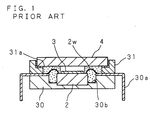
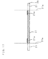
- FIG. 1 is a cross sectional view showing a schematic configuration of a prior art solid state imaging device.
- a solid state imaging device is described in Japanese Patent Application Laid-Open No. H06-021414.
- a hollow package is formed that comprises a space between a recess 30b which is provided approximately in the center of a base 30 and a light-transparent cover 4 which is attached to the base 30 with a frame 31 therebetween.
- a solid state image pickup device 2 is arranged in this space.
- the solid state image pickup device 2 is placed in the recess 30b provided approximately in the center of the base 30 composed of ceramic, plastic, or the like, while leads 30a extending outward from the periphery of the base 30 are attached to the base 30.
- the leads 30a composed of 42-alloy, copper, or the like are electrically connected through bonding wires 2w to the solid state image pickup device 2.
- a frame 31 having a predetermined height is attached on top of the leads 30a, while the light-transparent cover 4 composed of glass or the like is embedded in a cut-off section of the frame 31.
- a sealant 31a composed of epoxy resin is used in the adhesion between the frame 31 and the light-transparent cover 4, so as to seal the space formed between the light-transparent cover 4 and the recess 30b.
- This structure which seals the space formed between the light-transparent cover 4 and the recess 30b prevents moisture and dust in the outside from entering the space around the solid state image pickup device 2. At that time, the sealant 31a fills the space over the outside of the effective pixel region 3 of the solid state image pickup device 2.
- the method of fabrication of the solid state imaging device 1 is as follows.
- the solid state image pickup device 2 is mounted in the recess 30b of the base 30.
- the solid state image pickup device 2 is connected to the leads 30a with the bonding wires 2w.
- the frame 31 having a predetermined height is attached on top of the leads 30a.
- the light-transparent cover 4 composed of glass or the like is adhered to the cut-off section of the frame 31 with the sealant 31a.
- the sealant 31a is applied such as to fill the space over a predetermined region outside the effective pixel region 3 of the solid state image pickup device 2.
- the sealant 31a is cured completely so as to form a sealing structure in the region outside the effective pixel region 3 of the solid state image pickup device 2 in a state surrounding the bonding wires 2w, so as to seal the space formed between the light-transparent cover 4 and the recess 30b.
- the solid state imaging device 1 fabricated as such acquires light from the outside via the light-transparent cover 4, so that the effective pixel region 3 of the solid state image pickup device 2 receives the light.
- the light received in the effective pixel region 3 is converted into a predetermined electric signal by the solid state image pickup device 2, so that the electric signal is outputted through the bonding wires 2w and the leads 30a.
- the light-transparent cover 4 for protecting the effective pixel region 3 of the solid state image pickup device 2 against dust and damage has larger planar dimensions (size) than the solid state image pickup device 2 itself. That is, the above-mentioned structure that the light-transparent cover 4 covers not only the effective pixel region 3 alone but also the entirety, or even also the outer region, of the solid state image pickup device 2 is disadvantageous in the size reduction.
- the largeness of the area of the solid state imaging device 1 has restricted the size reduction of the solid state imaging device 1.
- a plurality of the solid state image pickup devices 2 formed simultaneously on a semiconductor wafer are divided into individual pieces using a dicing saw or the like.
- the divided solid state image pickup device 2 is mounted in a package or on a substrate, and then a light-transparent cover 4 is attached so as to cover the entirety, or even also the outer region, of the solid state image pickup device 2.
- a light-transparent cover 4 is attached so as to cover the entirety, or even also the outer region, of the solid state image pickup device 2.
- the light-transparent cover has larger planar dimensions than the solid state image pickup device itself. This has caused the problem that this largeness restricts the size reduction of the solid state imaging device. Further, in the prior art method of fabrication of the solid state imaging device, the light-transparent cover is attached after the solid state image pickup device has been divided into an individual piece. This has caused the problem that the reduction or avoidance of the occurrence of damage to the surface of the effective pixel region of the solid state image pickup device is notably difficult, and that the reduction of the fraction defective is limited.
- An object of the invention is to provide a solid state imaging device in which a light-transparent cover having planar dimensions smaller than those of a solid state image pickup device is adhered opposite to the effective pixel region in one surface of the solid state image pickup device, so as to protect the effective pixel region such as to prevent external influences (such as moisture and dust) from affecting the surface of the effective pixel region, and in which at the same time, the size of the solid state imaging device is reduced so that a solid state imaging device of a chip size having high reliability and high environmental durability is realized.
- Another object of the invention is to provide a semiconductor wafer on which a plurality of solid state image pickup devices are formed, in which a light-transparent plate or a light-transparent cover for protecting the surface of the effective pixel region of solid state image pickup device is formed before the dividing of the solid state image pickup devices into individual pieces, so as to permit easy storage and carriage and avoid the attachment of dust or the occurrence of damage to the surface of the effective pixel region after the process of dividing the solid state image pickup devices into individual pieces, so that the fraction defective is reduced in the process of assembling the solid state image pickup device especially after the dividing into individual pieces.
- Another object of the invention is to provide an optical device module such as a camera module permitting easy size reduction and having good portability by means of incorporating a solid state imaging device according to the invention.
- Another object of the invention is to provide a method of solid state imaging device fabrication, in which a light-transparent cover is adhered opposite to each effective pixel region so as to protect the effective pixel region of each of solid state image pickup devices formed on a semiconductor wafer, so that defects such as the attachment of dust and the occurrence of damage to the surface of the effective pixel region are avoided especially in the process of dividing of the solid state image pickup devices into individual pieces.
- Another object of the invention is to provide a method of solid state imaging device fabrication, in which a light-transparent plate is adhered opposite to the effective pixel regions so as to protect the effective pixel regions of solid state image pickup devices formed on a semiconductor wafer, and in which the light-transparent plate is then divided and thereby forms light-transparent covers, so as to avoid defects such as the attachment of dust and the occurrence of damage to the surface of the effective pixel region, so that the process of adhering the light-transparent covers to a plurality of solid state image pickup devices is achieved on a semiconductor wafer basis, and that high efficiency and productivity are obtained.
- Another object of the invention is to provide an optical device module and a method of its fabrication, in which an optical device module is fabricated with incorporating a solid state imaging device (solid state image pickup device) the effective pixel region of which is protected by a light-transparent cover, so as to permit size reduction (thickness reduction and weight reduction), yield improvement, process simplification, and price reduction.
- a solid state imaging device solid state image pickup device
- Another object of the invention is to provide an optical device module and a method of its fabrication, in which an optical device module is fabricated with incorporating a solid state imaging module component formed by integrating and resin-sealing a DSP (digital signal processor serving as an image processor) and a solid state imaging device (solid state image pickup device), so as to permit size reduction (thickness reduction and weight reduction), yield improvement, process simplification, and price reduction, as well as higher environmental durability (such as against moisture) and mechanical strength.
- a DSP digital signal processor serving as an image processor
- solid state imaging device solid state image pickup device
- Another object of the invention is to provide an optical device module and a method of its fabrication, in which a DSP (serving as an image processor) and a solid state imaging device (solid state image pickup device) are integrated onto a wiring board, and in which a sealing section for resin-sealing them is formed.
- a DSP serving as an image processor
- a solid state imaging device solid state image pickup device
- a solid state imaging device comprises: a solid state image pickup device having an effective pixel region in one surface thereof, a light-transparent cover arranged opposite to said effective pixel region and having planar dimensions smaller than those of said solid state image pickup device; and an adhering section for adhering said solid state image pickup device and said light-transparent cover.
- said adhering section contains photosensitive adhesive.
- a space is formed between said effective pixel region and said light-transparent cover, while said adhering section is formed outside said effective pixel region in said one surface of said solid state image pickup device.
- said adhering section seals the outer periphery of said space.
- a semiconductor wafer according to the invention on which a plurality of solid state image pickup devices each having an effective pixel region in one surface thereof are formed comprises: a light-transparent plate arranged opposite to said effective pixel region; and an adhering section for adhering said solid state image pickup device and said light-transparent plate.
- said light-transparent plate is divided so as to form light-transparent covers each having planar dimensions smaller than those of said solid state image pickup device.
- a semiconductor wafer according to the invention on which a plurality of solid state image pickup devices each having an effective pixel region in one surface thereof are formed comprises: a light-transparent cover arranged opposite to said effective pixel region; and an adhering section for adhering said solid state image pickup device and said light-transparent cover.
- said adhering section contains photosensitive adhesive.
- a space is formed between said effective pixel region and said light-transparent cover, while said adhering section is formed outside said effective pixel region in said one surface of said solid state image pickup device.
- said adhering section seals the outer periphery of said space.
- An optical device module comprises: a lens; a lens retainer for retaining said lens; and a solid state imaging device according to any specific one of the present invention, wherein said light-transparent cover is arranged opposite to said lens and inside said lens retainer.
- a method of solid state imaging device fabrication comprises the steps of forming a plurality of solid state image pickup devices each having an effective pixel region in one surface thereof, onto a semiconductor wafer; adhering a light-transparent cover having planar dimensions smaller than those of said solid state image pickup device, in a manner opposite to said effective pixel region onto said one surface; and dividing a plurality of said solid state image pickup devices onto each of which said light-transparent cover has been adhered, into individual solid state image pickup devices.
- a method of solid state imaging device fabrication according to the invention further comprises the step of dividing a light-transparent plate so as to form said light-transparent covers.
- adhesive is used that is patterned in a region outside said effective pixel region in said one surface of said solid state image pickup device.
- adhesive is used that is patterned on said light-transparent plate in correspondence to a region outside said effective pixel region in said one surface of said solid state image pickup device.
- the adhesive-patterned surface of said light-transparent plate is affixed onto a dicing tape, and then said light-transparent plate is divided so as to form said light-transparent covers.
- said adhesive contains photosensitive adhesive.
- a method of solid state imaging device fabrication comprises the steps of forming a plurality of solid state image pickup devices each having an effective pixel region in one surface thereof, onto a semiconductor wafer; adhering a light-transparent plate onto said one surface of said semiconductor wafer; dividing said light-transparent plate having been adhered onto said semiconductor wafer, so as to form light-transparent covers each being opposite to said effective pixel region; and dividing a plurality of said solid state image pickup devices into individual solid state image pickup devices.
- adhesive is used that is patterned in a region outside said effective pixel region in said one surface of said solid state image pickup device.
- adhesive is used that is patterned on said light-transparent plate in correspondence to a region outside said effective pixel region in said one surface of said solid state image pickup device.
- said adhesive contains photosensitive adhesive.
- An optical device module comprises: a wiring board on which wiring is formed; an image processor adhered to said wiring board and electrically connected to said wiring; a solid state imaging device in which a light-transparent cover having planar dimensions smaller than those of a solid state image pickup device is attached opposite to the effective pixel region of said solid state image pickup device, and which is adhered to said image processor and electrically connected to said wiring; and an optical path defining unit arranged opposite to said solid state imaging device and denning an optical path to said solid state imaging device.
- An optical device module comprises: a solid state imaging module component formed by resin-sealing: a module component wiring board on which wiring is formed; an image processor adhered to said module component wiring board and electrically connected to said wiring; and a solid state imaging device in which a light-transparent cover having planar dimensions smaller than those of a solid state image pickup device is attached opposite to the effective pixel region of said solid state image pickup device, and which is adhered to said image processor and electrically connected to said wiring; in the state that the surface of said light-transparent cover is exposed; and an optical path defining unit arranged opposite to said solid state imaging device and defining an optical path to said solid state imaging device.
- an external terminal connected to said wiring is formed on the surface of said module component wiring board reverse to the surface to which said image processor is adhered.
- said external terminal has a protruding shape.
- said optical device module further comprises a wiring board on which wiring is formed, while said external terminal of said module component wiring board is connected to said wiring of said wiring board.
- An optical device module comprises: a wiring board on which wiring is formed; an image processor adhered to said wiring board and electrically connected to said wiring; a solid state imaging device in which a light-transparent cover having planar dimensions smaller than those of a solid state image pickup device is attached opposite to the effective pixel region of said solid state image pickup device, and which is adhered to said image processor and electrically connected to said wiring; a sealing section for resin-sealing said wiring board, said image processor, and said solid state imaging device in the state that the surface of said light-transparent cover is exposed; and an optical path defining unit arranged opposite to said solid state imaging device and defining an optical path to said solid state imaging device.
- said optical path defining unit retains a lens arranged opposite to said light-transparent cover of said solid state imaging device.
- a method of optical device module fabrication comprises the steps of: adhering an image processor to a wiring board on which wiring is formed, and then connecting the connection terminals of said image processor to said wiring; adhering a solid state imaging device in which a light-transparent cover having planar dimensions smaller than those of a solid state image pickup device is attached opposite to the effective pixel region of said solid state image pickup device, to said image processor, and then connecting the connection terminals of said solid state imaging device to said wiring; and aligning said solid state imaging device and an optical path defining unit for defining an optical path to said solid state imaging device.
- a plurality of optical device modules are formed simultaneously on a multiple wiring board formed by linking a plurality of said wiring boards, while said multiple wiring board is then divided so that a plurality of said optical device modules are divided into individual optical device modules.
- a method of optical device module fabrication comprises the steps of adhering an image processor to a module component wiring board on which wiring is formed, and then connecting the connection terminals of said image processor to said wiring; adhering a solid state imaging device in which a light-transparent cover having planar dimensions smaller than those of a solid state image pickup device is attached opposite to the effective pixel region of said solid state image pickup device, to said image processor, and then connecting the connection terminals of said solid state imaging device to said wiring; resin-sealing said module component wiring board, said image processor, and said solid state imaging device in the state that the surface of said light-transparent cover is exposed, and thereby forming a solid state imaging module component; and aligning said solid state imaging device and an optical path defining unit for defining an optical path to said solid state imaging device.
- an external terminal is formed on the surface of said module component wiring board reverse to the surface to which said image processor is adhered, while said method further comprises the step of connecting said external terminal to said wiring formed on said wiring board.
- said external terminal has a protruding shape.
- a plurality of solid state imaging module components are formed simultaneously on a multiple module component wiring board formed by linking a plurality of said module component wiring boards, while said multiple module component wiring board is then divided so that a plurality of said solid state imaging module components are divided into individual solid state imaging module components.
- a plurality of optical device modules are formed simultaneously on a multiple wiring board formed by linking a plurality of said wiring boards, while said multiple wiring board is then divided so that a plurality of said optical device modules are divided into individual optical device modules.
- a method of optical device module fabrication comprises the steps of adhering an image processor to a wiring board on which wiring is formed, and then connecting the connection terminals of said image processor to said wiring; adhering a solid state imaging device in which a light-transparent cover having planar dimensions smaller than those of a solid state image pickup device is attached opposite to the effective pixel region of said solid state image pickup device, to said image processor, and then connecting the connection terminals of said solid state imaging device to said wiring; resin-sealing said wiring board, said image processor, and said solid state imaging device in the state that the surface of said light-transparent cover is exposed, and thereby forming a sealing section; and aligning said solid state imaging device and an optical path defining unit for defining an optical path to said solid state imaging device.
- a plurality of optical device modules are formed simultaneously on a multiple wiring board formed by linking a plurality of said wiring boards, while said multiple wiring board is then divided so that a plurality of said optical device modules are divided into individual optical device modules.
- the light-transparent cover for protecting the effective pixel region has planar dimensions smaller than those of the solid state image pickup device. This permits the size reduction of the solid state imaging device, and realizes a solid state imaging device of a chip size.
- the adhering section contains photosensitive adhesive. This permits the use of a photolithography technique, so as to realize precise pattern formation (shape and position) of the adhering section, and further permit simultaneous multiple formation.
- a space is formed over the surface of the effective pixel region. This prevents physical stress from acting on the effective pixel region. Further, the adhering section is formed outside the effective pixel region, and hence no optical material is arranged between the light-transparent cover and the effective pixel region. This avoids a reduction in the light transparency between the light-transparent cover and the effective pixel region.
- the adhering section seals the outer periphery of the space formed between the light-transparent cover and the effective pixel region. This prevents moisture and dust in the outside from entering the effective pixel region, and hence securely protects the effective pixel region, so as to permit a reliable and environment-durable solid state imaging device.
- a light-transparent plate, a light-transparent cover, or a light-transparent cover formed by dividing a light-transparent plate each for protecting the surface of the effective pixel region of the solid state image pickup device is formed before a plurality of the solid state image pickup devices formed on a semiconductor wafer are divided into individual pieces. This avoids the attachment of dust and the occurrence of a scratch in the surface of the effective pixel region after the process of dividing into individual pieces, so as to permit easy and safe storage and carriage in a semiconductor wafer state.
- an optical device module is fabricated with incorporating a solid state imaging device according to the invention. This permits a small optical device module having good portability.
- the light-transparent cover is adhered or formed to each solid state image pickup device in a semiconductor wafer state. This avoids the attachment of dust and the occurrence of a scratch in the surface of the effective pixel region after the process of deviding the solid state image picking device into individual pieces the fraction defective in the fabrication process of the solid state imaging device. Further, since the light-transparent cover is adhered individually to each solid state image pickup device, the adhesion of the light-transparent cover can be omitted for solid state image pickup devices having been determined as defective in advance. This improves the productivity.
- adhesive formed in a pattern on the solid state image pickup device on a semiconductor wafer, or alternatively on the light-transparent plate is used so as to adhere the light-transparent cover (light-transparent plate) for protecting the effective pixel region.
- This permits simultaneous pattern formation of the adhesive in a plurality of the solid state image pickup devices or in a plurality of the light-transparent covers, and hence improves the productivity.
- the light-transparent plate is divided in the state that the adhesive-patterned surface is affixed to a dicing tape. This permits the formation of the light-transparent covers with reducing the production of dust.
- the light-transparent plate is divided so as to form the light-transparent cover for each solid state image pickup device.
- This achieves simultaneous adhesion of the light-transparent covers to a plurality of solid state image pickup devices. That is, this simplifies the alignment of the light-transparent cover in comparison with the case that the light-transparent cover is adhered individually to each solid state image pickup device, so as to simplify the process and improve the productivity.
- the adhering section is formed on the semiconductor wafer so that the light-transparent plate is adhered, the alignment of the light-transparent plate is notably easy so that the light-transparent covers are formed efficiently.
- the solid state imaging device in which the light-transparent cover having planar dimensions smaller than those of the solid state image pickup device is attached (adhered by the adhering section) opposite to the effective pixel region of the solid state image pickup device is built into an optical device module.
- a solid state imaging module component formed by integrating and resin-sealing a DSP (serving as an image processor) and a solid state imaging device (solid state image pickup device) is used, so as to realize an optical device module having higher environmental durability (such as against moisture) and mechanical strength. Further, this permits the assembling process of the optical device module even in a production environment of lower cleanness. Since the solid state imaging module component comprises an external terminal capable of being connected to the outside by means of soldering or the like, this module component is easily assembled into another wiring board. This realizes an optical device module having high productivity.
- a DSP serving as an image processor
- a solid state imaging device solid state image pickup device
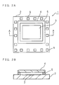
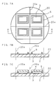
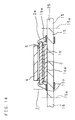
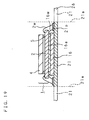
- FIGS. 2A and 2B are diagrams illustrating schematic configuration of a solid state imaging device according to Embodiment 1 of the invention.
- FIG. 2A is a plan view of the solid state imaging device viewed in a plane (one plane or one surface).
- FIG. 2B is a cross sectional view along the arrow line A-A in FIG. 2A.
- Numeral 1 indicates the solid state imaging device comprising: a solid state image pickup device 2 formed in a plan-view shape of a rectangle on a semiconductor substrate; a light-transparent cover 4 arranged opposite to an effective pixel region 3 in order to protect (the surface of) the effective pixel region 3 formed in one surface of the solid state image pickup device 2 against moisture, dust (particles and shavings), and the like in the outside; and an adhering section 5 formed outside the effective pixel region 3 in one surface of the solid state image pickup device 2 so as to adhere the light-transparent cover 4 and the solid state image pickup device 2.
- the solid state imaging device 1 acquires light from the outside via the light-transparent cover 4, so that the effective pixels (light-receiving elements) arranged in the effective pixel region 3 of the solid state image pickup device 2 receive the light.
- the light-transparent cover 4 is composed of a light-transparent material such as glass.
- the light-transparent cover 4 is arranged opposite to the effective pixel region 3 such as to cover at least the effective pixel region 3, and thereby protect the effective pixel region 3 against the outside.
- the light-transparent cover 4 has smaller planar dimensions (size) than the solid state image pickup device 2. This permits the size reduction of the solid state image pickup device 2.
- a space is preferably formed between the effective pixel region 3 and the light-transparent cover 4.
- the space formed between the effective pixel region 3 and the light-transparent cover 4 allows the light acquired from the outside via the light-transparent cover 4 to be incident directly on the effective pixel region 3. This avoids an optical loss along the optical path.
- Bonding pads 6 serving as terminals for connecting the solid state image pickup device 2 to an external circuit (not shown) are provided between the adhering section 5 (light-transparent cover 4) and the outer peripheral edges (chip edges) of the solid state image pickup device 2.
- the outer periphery of the space formed between the effective pixel region 3 and the light-transparent cover 4 arranged opposite to each other is preferably sealed completely by adhesive.
- the sealing of the outer periphery of the space formed between the effective pixel region 3 and the light-transparent cover 4 avoids the occurrence of defects in the effective pixel region 3 caused by the entering of moisture or the entering and adhering of dust into (the surface of) the effective pixel region 3 or by scratching the surface. This realizes a reliable solid state imaging device 1 at a high yield in the fabrication process.
- the solid state imaging device 1 When the solid state imaging device 1 is built into an optical device such as a camera and a video recorder camera, in addition to the protection of the surface of the effective pixel region 3 against dust and scratches, the light-transparent cover 4 need shut out infrared rays from the outside. In this case, an infrared cut-off film is easily formed on the surface of the light-transparent cover 4.
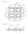
- FIGS. 3A-5B are diagrams illustrating a method of solid state imaging device fabrication according to Embodiment 2 of the invention. More specifically, FIGS. 3A-3E are diagrams illustrating the process of formation of light-transparent covers.
- FIGS. 4A and 4B are diagrams illustrating the situation of solid state image pickup devices formed on a semiconductor wafer.
- FIGS. 5A and 5B are diagrams illustrating the situation that the light-transparent covers formed in FIGS. 3A-3E are adhered to one surface (that has the effective pixel regions) of the solid state image pickup devices of FIGS. 4A and 4B.
- FIG. 3A shows a large-area light-transparent plate 10 composed of a glass plate or the like.
- the light-transparent plate 10 has a large area, and hence comprises a large number of cover corresponding regions 10b having boundaries indicated by dividing lines 10a.
- the area of the cover corresponding region 10b is adjusted appropriately such as to have the same planar dimensions as the light-transparent cover 4 when divided in a later process.
- FIG. 3B shows the situation that a large number of adhering sections 5 are formed simultaneously on the light-transparent plate 10.
- the adhering section 5 is patterned into an appropriate patterning shape correspondingly between the effective pixel region 3 and the bonding pads 6 serving as connection terminals to the outside.
- thermosetting resin such as an epoxy resin
- a large number of the adhering sections 5 are formed simultaneously on the light-transparent plate 10.
- This simultaneous formation of a large number of the adhering sections 5 on the light-transparent plate 10 improves the productivity.
- the purpose that the photosensitive adhesive is mixed into the thermosetting resin is to impart photosensitivity to the adhesive. This permits easy and precise patterning of the adhering sections 5 by means of the processing of the exposure and the development in the photolithography technique.
- the patterning of the adhering sections 5 can be carried out with precision. This permits precise formation of the adhering sections 5 even when the region outside the effective pixel region 3 is narrow.
- patterning methods for the adhering sections 5 include: the patterning of the adhesive (such as an epoxy resin) by means of a printing method; and the patterning of the adhesive by means of a dispenser method.
- the patterning method used for the adhering sections 5 may be any one selected appropriately depending on the necessity or suitability for the light-transparent plate 10, the solid state imaging device 1, and the adhesive.
- FIGS. 3C and 3D show the state that the light-transparent plate 10 on which a large number of the adhering sections 5 are patterned is diced along the dividing lines 10a, so that the cover corresponding regions 10b are divided into individual pieces so as to form light-transparent covers 4. That is, the surface of the light-transparent plate 10 on which the adhering sections 5 are formed is affixed to a dicing tape 12 fixed to a dicing ring 11. Then, a dicing saw 13 travels in the dicing direction 13a so as to divide the light-transparent plate 10 into the individual light-transparent covers 4.
- FIG. 3E shows the state that the light-transparent cover 4 on which the adhering section 5 is formed is removed from the dicing tape 12 under an appropriate condition.
- the adhering sections 5 formed on the light-transparent plate 10 are affixed to the dicing tape 12. This permits the formation of a hollow portion between the surface of the light-transparent plate 10 on which the adhering section 5 is formed and the dicing tape 12. This hollow portion serves as a space formed between the light-transparent cover 4 and the dicing tape 12, and thereby prevents the light-transparent cover 4 from contacting directly with the dicing tape 12 so as to prevent the light-transparent cover 4 from being contaminated with the dicing tape 12.
- the outer periphery of the hollow portion is surrounded and sealed by the adhering section 5 and the dicing tape 12. This prevents dust (such as shavings) generated in the dicing of the light-transparent plate 10 from attaching to the inner surface (the surface on which the adhering section 5 is formed) of the light-transparent cover 4. That is, it is avoided that when the light-transparent cover 4 is attached opposite to the surface of the effective pixel region 3 of the solid state image pickup device 2, the dust having been attached to the inner surface of the light-transparent cover 4 moves to the surface of the effective pixel region 3 of the solid state image pickup device 2.
- the dicing is carried out in the state that the surface of the light-transparent plate 10 reverse to the surface on which the adhering section 5 is formed is affixed to the dicing tape 12, the following problem occurs. That is, the inner surface (the surface on which the adhering section 5 is formed) of the light-transparent cover 4 is not sealed but open to the outside. This permits dust (such as shavings) generated in the dicing to attach to the inner surface of the light-transparent cover 4. Accordingly, when the light-transparent cover 4 is attached opposite to the surface of the effective pixel region 3 of the solid state image pickup device 2, the dust having been attached to the inner surface of the light-transparent cover 4 moves to the surface of the effective pixel region 3 of the solid state image pickup device 2. Further, in the surface reverse to the surface on which the adhering section 5 is formed, a blur can be formed by the adhesive of the dicing tape 12. This reduces the light transmissivity or its uniformity.
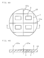
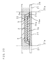
- FIG. 4A shows the state that a plurality of solid state image pickup devices 2 are formed simultaneously on a semiconductor wafer 20.
- Each solid state image pickup device 2 has an effective pixel region 3.
- Each solid state image pickup device 2 is defined by dividing lines 20a.
- FIG. 4B is a cross sectional view along the arrow line A-A in FIG. 4A.
- FIG. 5A shows the situation that light-transparent covers 4 (see FIG. 3E) formed in advance on appropriate regions outside the effective pixel regions 3 are adhered via the adhering sections 5 to one surface (that has the effective pixel regions 3) of the solid state image pickup devices 2 formed on the semiconductor wafer 20.
- Each light-transparent cover 4 is aligned appropriately to the region outside the effective pixel region 3 in the one surface of the solid state image pickup device 2, and then adhered using a method, such as infrared irradiation and thermal setting, appropriate to the property of the adhesive used in the adhering section 5.
- FIG. 5B is a cross sectional view along the arrow line A-A in FIG. 5A.
- the adhering section 5 seals completely the outer periphery of the space formed between the effective pixel region 3 and the light-transparent cover 4. This configuration avoids the occurrence of defects in the effective pixel region 3 caused by the entering of moisture or the entering and adhering of dust into (the surface of) the effective pixel region 3 or by scratching the surface. Further, since the adhesion of the light-transparent cover 4 (the formation of the adhering section 5) is carried out in the outside of the effective pixel region 3, no physical stress acts on the effective pixel region 3.
- the solid state image pickup devices 2 to which the light-transparent covers 4 are adhered are diced (divided) appropriately along the dividing lines 20a, and then removed from the semiconductor wafer 20, so that solid state imaging devices (1) are formed. It should be noted that in the surface on which the effective pixel region 3 is formed, regions for bonding pads (not shown) for connecting the solid state image pickup device 2 to an external circuit (not shown) and other regions are arranged outside the light-transparent cover 4 (adhering section 5). Further, the subsequent assembling process is carried out in the state that the effective pixel region 3 is protected. This avoids the possibility of damaging the effective pixel region 3 when the solid state imaging device (1) is transferred using a vacuum chuck handler or the like.
- FIGS. 6A-7C are diagrams illustrating a method of solid state imaging device fabrication according to Embodiment 3 of the invention. More specifically, FIGS. 6A and 6B are diagrams illustrating the process of formation of light-transparent covers. FIGS. 7A-7C are diagrams illustrating the process that the light-transparent covers formed in FIGS. 6A and 6B are adhered to one surface (that has the effective pixel regions) of the solid state image pickup devices formed on a semiconductor wafer.
- FIG. 6A shows a large-area light-transparent plate 10 composed of a glass plate or the like.
- the light-transparent plate 10 has a large area, and hence comprises a large number of cover corresponding regions 10b having boundaries indicated by dividing lines 10a.
- the area of the cover corresponding region 10b is adjusted appropriately such as to have the same planar dimensions as the light-transparent cover 4 when divided in a later process.
- FIG. 6B shows the state that the light-transparent plate 10 is diced along the dividing lines 10a, so that the cover corresponding regions (10b) are divided into individual pieces such as to form light-transparent covers 4. This division can be carried out using a dicing saw similarly to Embodiment 2.
- FIG. 7A shows the state that adhering sections 5 are patterned in the regions outside the effective pixel regions 3 of the solid state image pickup devices 2 in one surface (that has the effective pixel regions 3) of the semiconductor wafer 20 on which a large number of solid state image pickup devices 2 are formed simultaneously.
- FIG. 7B is a cross sectional view along the arrow line A-A in FIG. 7A.
- Adhesive in which photosensitive adhesive and thermosetting resin are mixed is uniformly applied onto the surface of the semiconductor wafer 20 on which the solid state image pickup devices 2 are formed. Then, the adhesive is patterned by means of a known photolithography technique, so that the adhering section 5 is formed in each solid state image pickup device 2.
- the adhering sections 5 are formed simultaneously in a plurality of the solid state image pickup devices 2 having been formed simultaneously on the semiconductor wafer 20. This simultaneous formation of a large number of the adhering sections 5 improves the productivity. It should be noted that in the surface on which the effective pixel region 3 is formed, regions for bonding pads (not shown) for connecting the solid state image pickup device 2 to an external circuit (not shown) and other regions are arranged outside the adhering section 5.
- FIG. 7C shows the state that light-transparent covers 4 (see FIG. 6B) formed in advance are adhered to the adhering sections 5 of the solid state image pickup devices 2 formed on the semiconductor wafer 20.
- Each light-transparent cover 4 is aligned and placed on the adhering section 5, and then adhered to the adhering section 5 by infrared irradiation or thermal setting.
- the adhering section 5 seals completely the outer periphery of the space formed between the effective pixel region 3 and the light-transparent cover 4. This configuration avoids the occurrence of defects in the effective pixel region 3 caused by the entering of moisture or the entering and adhering of dust into (the surface of) the effective pixel region 3 or by scratching the surface.
- the solid state image pickup devices 2 to which the light-transparent covers 4 are adhered are diced (divided) appropriately along the dividing lines 20a, and then removed from the semiconductor wafer 20, so that solid state imaging devices (1) are formed.
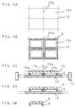
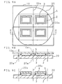
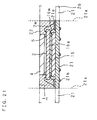
- FIGS. 8A-9C are diagrams illustrating a method of solid state imaging device fabrication according to Embodiment 4 of the invention. More specifically, FIGS. 8A and 8B are diagrams illustrating the state that adhering sections are formed in one surface (that has the effective pixel regions) of solid state image pickup devices formed on a semiconductor wafer. FIGS. 9A-9C are diagrams illustrating the process that after a light-transparent plate is adhered to the semiconductor wafer of FIGS. 8A and 8B, the light-transparent plate is divided so as to form light-transparent covers.
- FIG. 8A shows the state that adhering sections 5 are patterned in the regions outside the effective pixel regions 3 of the solid state image pickup devices 2 in one surface (that has the effective pixel regions 3) of the semiconductor wafer 20 on which a large number of solid state image pickup devices 2 are formed simultaneously.
- FIG. 8B is a cross sectional view along the arrow line A-A in FIG. 8A. This state is the same as that of FIGS. 7A and 7B of Embodiment 3.
- the process conditions such as the adhesive are also the same as those of the other embodiments.
- FIG. 9A shows the state that a light-transparent plate 10 is adhered to the semiconductor wafer 20 of FIGS. 8A and 8B in which the adhering sections 5 are formed on the solid state image pickup devices 2.
- the light-transparent plate 10 is placed appropriately on the adhering sections 5 of the semiconductor wafer 20, and then adhered to the adhering sections 5 by infrared irradiation or thermal setting. Since the adhering section 5 is formed in advance on each solid state image pickup device 2, precise alignment of the light-transparent plate 10 is not necessary. Further, general alignment is sufficient between the semiconductor wafer 20 and the light-transparent plate 10. That is, individual alignment of the light-transparent plate 10 to each solid state image pickup device 2 is unnecessary.
- FIG. 9B is a cross sectional view along the arrow line A-A in FIG. 9A.
- the entirety of the semiconductor wafer 20 is adhered to and covered with the light-transparent plate 10. This permits storage and carriage in the state that the effective pixel regions are securely protected.
- the adhering section 5 seals completely the outer periphery of the space formed between the effective pixel region 3 and the light-transparent cover 4. This configuration avoids the occurrence of defects in the effective pixel region 3 caused by the entering of moisture or the entering and adhering of dust into (the surface of) the effective pixel region 3 or by scratching the surface.
- FIG. 9C shows the state that the light-transparent plate 10 adhered to the semiconductor wafer 20 is diced appropriately along the dividing lines 10a, so as to form light-transparent covers 4. That is, after the light-transparent plate 10 is adhered to the semiconductor wafer 20, the light-transparent plate 10 is divided so as to form the light-transparent covers 4.
- the solid state image pickup devices 2 to which the light-transparent covers 4 are adhered are diced (divided) appropriately along the dividing lines 20a, and then removed from the semiconductor wafer 20, so that solid state imaging devices (1) are formed.
- the method described here is that the adhering sections 5 are patterned on the solid state image pickup devices 2 (see FIG. 8B) so that the semiconductor wafer 20 and the light-transparent plate 10 are adhered to each other, and that the light-transparent plate 10 is then diced so as to form the light-transparent covers 4.
- an alternative method may be used that the adhering sections 5 are patterned on the light-transparent plate 10 (see FIG. 3B) so that the semiconductor wafer 20 and the light-transparent plate 10 are adhered to each other, and that the light-transparent plate 10 is then diced so as to form the light-transparent covers 4.
- the adhering sections 5 formed on the light-transparent plate 10 are aligned appropriately to the effective pixel regions 3 of the solid state image pickup devices 2.
- the configuration of the effective pixel region 3 prevents the shavings generated in the dicing from entering the region (that is, the adhering section 5 seals the outer periphery of the effective pixel region 3, and the like). Further, before the solid state image pickup devices 2 are divided into individual pieces, the light-transparent covers 4 are adhered and formed opposite to the effective pixel regions 3. This avoids defects such as the attachment of dust and the occurrence of damage to the surface of the effective pixel regions 3 in the processes after the dividing of the solid state image pickup devices 2 into individual pieces, so that the fraction defective is reduced in the process of assembling the solid state image pickup devices 2 especially after the dividing into individual pieces.
- planar dimensions of the light-transparent cover 4 are smaller than those of the solid state image pickup device 2. This realizes a small solid state imaging device (1) of a chip size or the like. In the processes after the light-transparent cover 4 is adhered, the cleanness of the surroundings (production environment) does not need strict control. This simplifies the process, and hence reduces fabrication cost.
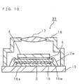
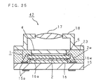
- FIG. 10 is a cross sectional view showing schematic configuration of an optical device module according to Embodiment 5 of the invention.
- the optical device module 39 is, for example, a camera module.
- a lens 17 for acquiring the outside light onto a wiring board 15 and a lens retainer 18 for retaining the lens 17 are attached to a wiring board 15.
- a digital signal processor (DSP, hereafter) 16 is mounted on the wiring board 15 composed of a printed wiring board or a ceramic substrate.
- the DSP 16 serves as a controlling section (image processor) which controls the operation of a solid state imaging device 1 (solid state image pickup device 2), and processes appropriately a signal outputted from the solid state imaging device 1 (solid state image pickup device 2) so as to generate a necessary signal to the optical device.
- Connection terminals of the DSP 16 are wire-bonded by bonding wires 16w to wiring (not shown) formed on the wiring board 15, so as to be connected electrically.
- a solid state image pickup device 2 of the present invention is mounted via a spacer 16a on the DSP 16 fabricated in the form of a semiconductor chip. Connection terminals (bonding pads 6, see FIG. 2A) of the solid state image pickup device 2 are wire-bonded by bonding wires 2w to wiring (not shown) formed on the wiring board 15, so as to be connected electrically.
- a light-transparent cover 4 is adhered by an adhering section 5 to the solid state image pickup device 2 according to the invention, while the light-transparent cover 4 is arranged opposite to the lens 17. That is, the solid state image pickup device 2 is arranged inside the lens retainer 18. Further, the planar dimensions of the light-transparent cover 4 are smaller than those of the solid state image pickup device 2. This permits the size reduction of the lens retainer to a practical limit, and hence realizes a small solid state imaging device of a chip size or the like.
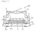
- FIG. 11 is a cross sectional view showing schematic configuration of an optical device module according to Embodiment 6 of the invention.
- Like parts to Embodiments 1-5 are designated by like numerals, and hence detailed description is omitted. Further, its plan view is omitted. However, its basic plan-view shape is a rectangle (a square or a genuine rectangle), and may be changed appropriately when necessary.
- the optical device module 40 comprises: a wiring board 15 on which wiring 15p is formed; a solid state imaging device 1; a DSP 16 serving as an image processor which controls the operation of the solid state imaging device 1 (solid state image pickup device 2), and processes a signal outputted from the solid state imaging device 1; and a lens retainer 18 arranged opposite to the solid state imaging device 1 and serving as an optical path defining unit for defining an optical path to the solid state imaging device 1.
- the solid state imaging device 1 has the configuration of Embodiment 1, and is fabricated by the method of fabrication according to Embodiments 2-4.
- the configuration and the method of fabrication of the solid state imaging device 1 are not limited to those of Embodiments 1-4.
- the solid state imaging device 1 may have any configuration as long as the light-transparent cover 4 having planar dimensions smaller than those of the solid state image pickup device 2 is attached (adhered by the adhering section 5) opposite to the effective pixel region (3) of the solid state image pickup device 2.
- the optical device module 40 is generally assembled as follows. First, the DSP 16 is placed and adhered (die-bonded) on the wiring board 15 on which the wiring 15p is formed. Then, the connection terminals of the DSP 16 are connected by the bonding wires 16w to the wiring 15p formed on the wiring board 15. After that, the solid state imaging device 1 (the surface of the solid state image pickup device 2 on which the light-transparent cover 4 is not attached) is stacked (placed) and adhered (die-bonded) on the DSP 16 via the spacer 16a composed of an insulating sheet.
- connection terminals of the solid state imaging device 1 are connected by the bonding wires 2w to the wiring 15p.
- the DSP 16 is preferably in the form of a semiconductor chip (bare chip) from the perspective of size reduction. However, the DSP 16 may be packaged (resin-sealed) using a chip-size package technique or the like. When the DSP 16 is packaged, the spacer 16a and the bonding wires 16w are unnecessary. In this case, the connection terminals extracted from the package are connected directly to the wiring 15p, while the solid state imaging device 1 is adhered directly on the package.
- the solid state imaging device 1 (light-transparent cover 4) and the lens retainer 18 are aligned (positioned) opposite to each other. Then, the lens retainer 18 and the wiring board 15 are linked (by adhesion, fitting, or the like) to each other, so that the optical device module 40 is completed.
- the lens retainer 18 has the function of an optical path defining unit for defining the optical path to the solid state imaging device 1 (light-transparent cover 4) and the function of protecting means for protecting the solid state imaging device 1, the DSP 16, and the like against the outer environment.
- the lens 17 and the lens retainer 18 are preferable integrated to each other. However, the invention is not limited to this, and the lens 17 may be assembled separately from the lens retainer 18. This configuration that the lens 17 is assembled separately permits an arbitrary change in the specification of the lens, and hence realizes an optical device module having wider universality.
- the light-transparent cover 4 having planar dimensions smaller than those of the solid state image pickup device 2 is attached opposite to the effective pixel region (3) of the solid state image pickup device 2. This allows the shape of the lens retainer 18 to approach the chip size of the solid state image pickup device 2, and hence realizes a small optical device module. In particular, when used as a camera module, this optical device module serves as a small camera having good portability.
- the light projected from an object through the lens 17 onto the solid state imaging device 1 (solid state image pickup device 2) is converted into an electric signal.
- the DSP 16 performs digital processing on this electric signal, and then outputs the signal.
- the optical device module 40 outputs the signal to the outside via the wiring 15p formed on the surface of the wiring board 15 reverse to the surface on which the DSP 16 is mounted.
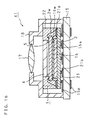
- FIGS. 12-15 are process diagrams showing cross sectional views of the fabrication processes of an optical device module according to Embodiment 6 of the invention. The fabrication processes of the optical device module 40 are described below in further detail with reference to FIGS. 12-15.
- FIG. 12 shows a multiple wiring board 25 formed by linking a plurality of wiring boards 15.
- the multiple wiring board 25 is formed by linking a plurality of wiring boards 15 each corresponding to an optical device module 40, in the shape of a matrix, a long sheet, or the like.
- the use of the multiple wiring board 25 permits simultaneous fabrication of a plurality of the optical device modules 40 each corresponding to each wiring board 15.
- Regions each corresponding to a wiring board 15 are defined along the dividing lines 15a on the multiple wiring board 25, and divided eventually along the dividing lines 15a into individual wiring boards 15 (individual optical device modules 40). Described below are the processes of simultaneous fabrication of a plurality of optical device modules 40 by using the multiple wiring board 25. However, in place of the use of the multiple wiring board 25, the optical device module 40 may be fabricated using an intrinsically separated wiring board 15.
- the multiple wiring board 25 is composed of a ceramic substrate, a glass epoxy substrate, an alumina substrate, or the like.
- the multiple wiring board 25 has a thickness of 0.05-2.00 mm or the like from the perspective of mechanical strength.
- wiring 15p is formed (patterned) in correspondence to each wiring board 15.
- the figure shows the case that the wiring 15p is formed on both sides of the multiple wiring board 25.
- the wiring 15p may be formed only on one side of the multiple wiring board 25. However, from the perspective of assembling density, it is preferable that the wiring 15p is formed on both sides, so that terminals are extracted from both sides of the wiring board 15, that is, from the side on which solid state imaging device 1 is mounted and its reverse side.
- the wiring 15p sections formed on both sides are connected to each other in the inside of the wiring board 15 (not shown).
- the wiring 15p is designed appropriately depending on the required specification of the optical device module 40. Since adjacent wiring boards 15 linked to each other are processed similarly and simultaneously, the fabrication processes are described only for one wiring board 15, and hence description for the other wiring boards 15 is omitted appropriately.
- FIG. 13 shows the situation of assembling of the DSP 16.
- the DSP 16 is placed and adhered by die-bonding on the surface of the wiring board 15 (multiple wiring board 25) on which the wiring 15p is formed. Then, (the connection terminals of) the DSP 16 is wire-bonded and connected electrically by the bonding wires 16w to the wiring 15p.
- the method of connection used here may be flip chip bonding in place of the wire bonding.
- FIG. 14 shows the situation of assembling of the solid state imaging device 1.
- the spacer 16a composed of an insulating sheet is placed and adhered on the DSP 16.
- the spacer 16a preferably has somewhat buffering property in order to avoid any influence to the surface of the DSP 16 during the adhesion.
- the spacer 16a is composed of a sheet of acrylic resin or the like having a thickness of 0.05-1.00 mm.
- FIG. 15 shows the situation of assembling of the lens retainer 18.
- the lens retainer 18 (lens 17) and the solid state imaging device 1 are aligned appropriately to each other. Then, the lens retainer 18 is adhered to the wiring board 15 using adhesive resin.
- the lens retainer 18 and the wiring board 15 may be linked (fixed) to each other using another means such as a screw and a mating mechanism.
- the lens 17 is preferably integrated into the lens retainer 18. However, the lens 17 may be assembled separately.
- the lens retainer 18 has the function of allowing the light from the object to be incident on the solid state imaging device 1 (solid state image pickup device 2) and the function of shutting out the light other than that from the object, so as to define a desired optical path. Further, the lens retainer 18 may have the function of a shutter for shutting out the light from the object which is otherwise to be incident on the solid state image pickup device 2.
- a plurality of optical device modules 40 (of integrated lens type) corresponding to the respective wiring boards 15 are formed on the multiple wiring board 25.
- a plurality of the optical device modules 40 formed on the multiple wiring board 25 are divided (cut out) into individual pieces along the dividing lines 15a using a dicing machine, a router, a metal mold press, or the like.
- individual optical device modules 40 (FIG. 11) are formed.
- the lens retainers 18 are those separated from each other in correspondence to the respective wiring boards 15.
- a multiple lens retainer formed by linking a plurality of lens retainers 18 may be used corresponding to the multiple wiring board 25. The use of the multiple lens retainer simplifies further the process of alignment between the lens retainer 18 and the solid state imaging device 1.
- the solid state imaging device in which the light-transparent cover having planar dimensions smaller than those of the solid state image pickup device is attached (adhered by the adhering section) opposite to the effective pixel region of the solid state image pickup device is built into the optical device module.
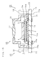
- FIG. 16 is a cross sectional view showing schematic configuration of an optical device module according to Embodiment 7 of the invention.
- Like parts to Embodiments 1-6 are designated by like numerals, and hence detailed description is omitted. Further, its plan view is omitted. However, its basic plan-view shape is a rectangle (a square or a genuine rectangle), and may be changed appropriately when necessary.
- the optical device module 41 comprises: a module component wiring board 21 on which wiring 21p is formed; a solid state imaging device 1; a DSP 16 serving as an image processor; a solid state imaging module component 22 in which the module component wiring board 21, the DSP 16, and the solid state imaging device 1 are resin-sealed in the state that the surface of the light-transparent cover 4 is exposed; and a lens retainer 18 arranged opposite to the solid state imaging device 1 and serving as an optical path defining unit for defining an optical path to the solid state imaging device 1.
- the optical device module 41 may further comprise a wiring board 15 when appropriate.
- the solid state imaging device 1 has the same configuration as that of Embodiment 6.
- the solid state imaging device 1 may have any configuration as long as the light-transparent cover 4 having planar dimensions smaller than those of the solid state image pickup device 2 is attached (adhered by the adhering section 5) opposite to the effective pixel region (3) of the solid state image pickup device 2.
- the optical device module 41 is generally assembled as follows. First, the DSP 16 is placed and adhered (die-bonded) on the module component wiring board 21 on which the wiring 21p is formed. Then, the connection terminals of the DSP 16 are connected by the bonding wires 16w to the wiring 21p formed on the module component wiring board 21. After that, the solid state imaging device 1 (the surface of the solid state image pickup device 2 on which the light-transparent cover 4 is not attached) is stacked (placed) and adhered (die-bonded) on the DSP 16 via the spacer 16a composed of an insulating sheet. Then, the connection terminals of the solid state imaging device 1 (solid state image pickup device 2) are connected by the bonding wires 2w to the wiring 21p.
- the surface of the module component wiring board 21 on which the DSP 16 is adhered, the DSP 16, and the solid state imaging device 1 are resin-sealed in the state that the surface of the light-transparent cover 4 is exposed, so that the solid state imaging module component 22 is formed. Since the module component wiring board 21, the DSP 16, and the solid state imaging device 1 are resin-sealed into the solid state imaging module component 22, the DSP 16 is preferably in the form of a semiconductor chip (bare chip) from the perspective of size reduction.
- the lens retainer 18 may be linked (by adhesion, fitting, or the like) to the solid state imaging module component 22 in place of the wiring board 15. Further, the lens retainer 18 may be linked to both of the wiring board 15 and the solid state imaging module component 22. In either case, alignment is necessary between the solid state imaging module component 22 (solid state imaging device 1) and the lens retainer 18 serving as the optical path defining unit.
- the surface of the module component wiring board 21 on which the DSP 16 is adhered is resin-sealed and thereby integrated (packaged) with the DSP 16 and the solid state imaging device 1.
- the solid state imaging module component 22 is preferably formed (resin-sealed) using a chip-size package technique, while the external terminals 21b connected to the wiring 21p are formed on the surface reverse to the surface on which the DSP 16 is adhered. This resin sealing of the solid state imaging module component 22 by the chip-size package technique permits further size reduction.
- the solid state imaging module component 22 serves also as protecting means for protecting securely these bare chips against the outer environment, so as to improve environmental durability (such as against moisture).
- the solid state imaging module component 22 is preferably in the form of a chip-size package from the perspective of size reduction. However, another method may be used in the integrating and packaging.
- the external terminals 21b of the module component wiring board 21 are formed in a protruding shape, connection to the outside (such as the wiring board 15) becomes easy.
- the use of the wiring board 15 in addition to the module component wiring board 21 ensures the mechanical strength of the optical device module.
- the lens retainer 18 may be linked to the solid state imaging module component 22, while the external terminals 21b may be connected to flexible film wiring or the like in place of the wiring board 15 when appropriate.
- the light-transparent cover 4 having planar dimensions smaller than those of the solid state image pickup device 2 is attached opposite to the effective pixel region (3) of the solid state image pickup device 2. This allows the shape of the lens retainer 18 to approach the chip size of the solid state image pickup device 2, and hence realizes a small optical device module. In particular, when used as a camera module, this optical device module serves as a small camera having good portability.
- the optical device module 41 the light projected from an object through the lens 17 onto the solid state imaging device 1 (solid state image pickup device 2) is converted into an electric signal.
- the DSP 16 performs digital processing on this electric signal, and then outputs the signal.
- the optical device module 41 outputs the signal via the external terminals 21b of the module component wiring board 21 or via the wiring 15p formed on the surface of the wiring board 15 reverse to the surface on which the solid state imaging module component 22 is mounted.
- FIGS. 17-24 are process diagrams showing cross sectional views of the fabrication processes of an optical device module according to Embodiment 7 of the invention.
- the fabrication processes of the optical device module 41 are described below in further detail with reference to FIGS. 17-24.
- FIG. 17 shows a multiple module component wiring board 26 formed by linking a plurality of module component wiring boards 21.
- the multiple module component wiring board 26 is formed by linking a plurality of module component wiring boards 21 each corresponding to a solid state imaging module component 22 (serving as a component of an optical device module 41), in the shape of a matrix, a long sheet, or the like.
- the use of the multiple module component wiring board 26 permits simultaneous fabrication of a plurality of the solid state imaging module components 22 each corresponding to each module component wiring board 21.
- Regions each corresponding to a module component wiring board 21 are defined along the dividing lines 21a on the multiple module component wiring board 26, and divided eventually along the dividing lines 21a into individual module component wiring boards 21 (individual solid state imaging module components 22). Described below are the processes of simultaneous fabrication of a plurality of solid state imaging module components 22 by using the multiple module component wiring board 26. However, in place of the use of the multiple module component wiring board 26, the solid state imaging module component 22 may be fabricated using an intrinsically separated module component wiring board 21.
- the multiple module component wiring board 26 is preferably composed of polyimide resin or the like the thickness of which is easily reduced.
- the multiple module component wiring board 26 has a thickness of 0.025-1.00 mm or the like.
- wiring 21p is formed (patterned) in correspondence to each module component wiring board 21.
- the figure shows the case that the wiring 21p is formed only on one side (the upper surface in the figure) of the module component wiring board 21.
- the external terminals 21b are formed on the other side of the module component wiring board 21, wiring for the formation of the external terminals 21b is formed also on this other side appropriately (not shown).
- the wiring 21p When the wiring 21p is formed on both sides, the wiring 21p sections formed on both sides are connected to each other in the inside of the module component wiring board 21 (not shown).
- the wiring 21p is designed appropriately depending on the required specification of the solid state imaging module component 22 (corresponding to the optical device module 41). Since adjacent module component wiring boards 21 linked to each other are processed similarly and simultaneously, the fabrication processes are described only for one module component wiring board 21, and hence description for the other module component wiring boards 21 is omitted appropriately.
- FIG. 18 shows the situation of assembling of the DSP 16.
- the DSP 16 is placed and adhered by die-bonding on the surface of the module component wiring board 21 (multiple module component wiring board 26) on which the wiring 21p is formed. Then, (the connection terminals of) the DSP 16 is wire-bonded and connected electrically by the bonding wires 16w to the wiring 21p.
- the method of connection used here may be flip chip bonding in place of the wire bonding.
- FIG. 19 shows the situation of assembling of the solid state imaging device 1.
- the solid state imaging device 1 is assembled similarly to Embodiment 6, and hence detailed description is omitted.
- FIG. 20 shows the situation of resin sealing of the solid state imaging module component 22.
- the surface of the module component wiring board 21 on which the DSP 16 is adhered is resin-sealed together with the DSP 16 and the solid state imaging device 1, so that the solid state imaging module component 22 is formed. At that time, the surface of the light-transparent cover 4 of the solid state imaging device 1 is exposed.
- the sealing resin used here may be an appropriate epoxy resin used in ordinary chip-size packaging or the like. From the perspective of the simplicity in the sealing process, adjacent module component wiring boards 21 (solid state imaging module components 22) in the multiple module component wiring board 26 are preferably resin-sealed in an integrated manner as shown in the figure. However, an appropriate spacer (such as a metal mold) may be arranged in advance along the dividing lines 21a, so that the sealing resin may be formed in an intrinsically separated manner.
- FIG. 21 shows the situation of the formation of the external terminals 21b of the solid state imaging module component 22.
- the external terminals 21b connected to the wiring 21p are formed on the surface of the module component wiring board 21 reverse to the surface on which the DSP 16 is adhered.
- the wiring 21p and the external terminals 21b are connected to each other in the inside of the module component wiring board 21 (not shown).
- the external terminal 21b has the protruding shape of a solder ball, so as to permit easy connection to the wiring board 15 or the like.
- a solder bump may be used in place of the solder ball.
- the external terminals 21b may be composed of gold or the like in place of the solder.
- a plurality of the solid state imaging module components 22 formed on the multiple module component wiring board 26 are divided along the dividing lines 21a.
- Adjacent solid state imaging module components 22 (module component wiring boards 21) resin-sealed in an integrated manner on the multiple module component wiring board 26 are divided (cut out) into individual pieces using a dicing machine, a router, a metal mold press, or the like.
- individual solid state imaging module components 22 (FIG. 22) serving as intermediate components are formed.
- the use of the multiple module component wiring board 26 permits simultaneous fabrication of a plurality of the solid state imaging module components 22, and hence improves further the production efficiency of the solid state imaging module component 22. Further, this achieves uniformity in the characteristics of the solid state imaging module components 22. This improves further the production efficiency of the optical device module 41, and achieves uniformity in the characteristics of the optical device modules 41.
- FIG. 22 shows the solid state imaging module component 22.
- the solid state imaging module component 22 is surrounded by the module component wiring board 21 and the sealing resin, and hence hardly affected by the outer environment. This permits size reduction, and also improves environmental durability (such as against moisture) and mechanical strength.
- FIG. 23 shows the situation of assembling of the solid state imaging module component 22 onto the multiple wiring board 25 formed by linking a plurality of wiring boards 15.
- the use of the multiple wiring board 25 permits simultaneous fabrication of a plurality of the optical device modules 41 each corresponding to each wiring board 15.
- the multiple wiring board 25 is described in Embodiment 6, and hence detailed description is omitted. Described below are the processes of simultaneous fabrication of a plurality of optical device modules 41 by using the multiple wiring board 25. However, in place of the use of the multiple wiring board 25, the optical device module 41 may be fabricated using an intrinsically separated wiring board 15.
- the wiring 15p is adhered (connected) to the external terminals 21b.
- the method of this connection may be soldering.
- Other applicable methods of adhesion (connection) include an electro-conductive adhesive and an anisotropic electro-conductive material. Since adjacent wiring boards 15 linked to each other are processed similarly and simultaneously, the fabrication processes are described only for one wiring board 15, and hence description for the other wiring boards 15 is omitted appropriately.
- FIG. 24 shows the situation of assembling of the lens retainer 18.
- the lens retainer 18 (lens 17) and the solid state imaging module component 22 (solid state imaging device 1) are aligned appropriately to each other. Then, the lens retainer 18 is adhered to the wiring board 15 using adhesive resin.
- the method of attachment (linkage) is the same as that of Embodiment 6, and hence detailed description is omitted.
- a plurality of optical device modules 41 (of integrated lens type) corresponding to the respective wiring boards 15 are formed on the multiple wiring board 25.
- a plurality of the optical device modules 41 formed on the multiple wiring board 25 are divided (cut out) into individual pieces along the dividing lines 15a using a dicing machine, a router, a metal mold press, or the like. As a result, individual optical device modules 41 (FIG. 16) are formed.
- the lens retainer 18 is linked to the wiring board 15.
- another portion may be linked.
- the lens retainer 18 may be linked to both of the wiring board 15 and the solid state imaging module component 22.
- the lens retainer 18 may be linked to the solid state imaging module component 22.
- the solid state imaging module component 22 may be linked to the wiring board 15.
- any kind of linkage may be used as long as the alignment of the solid state imaging module component 22 (solid state imaging device 1) is ensured relative to the lens retainer 18 for defining an optical path to the solid state imaging device 1. Further, a multiple lens retainer formed by linking a plurality of lens retainers 18 may be used similarly to Embodiment 6.
- the solid state imaging device in which the light-transparent cover having planar dimensions smaller than those of the solid state image pickup device is attached (adhered by the adhering section) opposite to the effective pixel region of the solid state image pickup device is built into the optical device module.
- a multiple wiring board formed by linking a plurality of wiring boards is used. This permits simultaneous fabrication of a plurality of optical device modules, and hence improves further the production efficiency of the optical device module. Further, this achieves uniformity in the characteristics of the optical device modules.
- a solid state imaging module component formed by integrating and resin-sealing a DSP (serving as an image processor) and a solid state imaging device (solid state image pickup device) is used, so as to realize an optical device module having higher environmental durability (such as against moisture) and mechanical strength. Further, this permits the assembling process of the optical device module even in a production environment of lower cleanness. Since the solid state imaging module component comprises external terminals capable of being connected to the outside by means of soldering or the like, this module component is easily assembled into another wiring board. This realizes an optical device module having high productivity.
- FIG. 25 is a cross sectional view showing schematic configuration of an optical device module according to Embodiment 8 of the invention.
- Like parts to Embodiments 1-7 are designated by like numerals, and hence detailed description is omitted. Further, its plan view is omitted. However, its basic plan-view shape is a rectangle (a square or a genuine rectangle), and may be changed appropriately when necessary.
- the optical device module 42 comprises: a wiring board 15 on which wiring 15p is formed; a solid state imaging device 1; a DSP 16 serving as an image processor which controls the operation of the solid state imaging device 1 (solid state image pickup device 2), and processes a signal outputted from the solid state imaging device 1; a sealing section 23 for resin-sealing the wiring board 15, the DSP 16, and the solid state imaging device 1 in the state that the light-transparent cover 4 is exposed; and a lens retainer 18 arranged opposite to the solid state imaging device 1 and serving as an optical path defining unit for defining an optical path to the solid state imaging device 1.
- the solid state imaging device 1 has the same configuration as that of Embodiment 6.
- the solid state imaging device 1 may have any configuration as long as the light-transparent cover 4 having planar dimensions smaller than those of the solid state image pickup device 2 is attached (adhered by the adhering section 5) opposite to the effective pixel region (3) of the solid state image pickup device 2.
- the optical device module 42 is generally assembled as follows. First, the DSP 16 is placed and adhered (die-bonded) on the wiring board 15 on which the wiring 15p is formed. Then, the connection terminals of the DSP 16 are connected by the bonding wires 16w to the wiring 15p formed on the wiring board 15. After that, the solid state imaging device 1 (the surface of the solid state image pickup device 2 on which the light-transparent cover 4 is not attached) is stacked (placed) and adhered (die-bonded) on the DSP 16 via the spacer 16a composed of an insulating sheet. Then, the connection terminals of the solid state imaging device 1 (solid state image pickup device 2) are connected by the bonding wires 2w to the wiring 15p.
- the DSP 16 is preferably in the form of a semiconductor chip (bare chip) from the perspective of size reduction.
- the DSP 16 may be packaged (resin-sealed) using a chip-size package technique or the like.
- the spacer 16a and the bonding wires 16w are unnecessary.
- the connection terminals extracted from the package are connected directly to the wiring 15p, while the solid state imaging device 1 is adhered directly on the package.
- the sealing section 23 is formed that resin-seals the surface of the wiring board 15 on which the DSP 16 is adhered, the DSP 16, and the solid state imaging device 1 in the state that the surface of the light-transparent cover 4 is exposed. Then, the solid state imaging device 1 (light-transparent cover 4) and the lens retainer 18 are aligned (positioned) opposite to each other. Then, the lens retainer 18 and the sealing section 23 are linked (by adhesion, fitting, or the like) to each other, so that the optical device module 42 is completed. Since the DSP 16 and the solid state imaging device 1 are resin-sealed, the DSP 16 is preferably in the form of a semiconductor chip (bare chip) from the perspective of size reduction. The configuration and the functions of the lens retainer 18 (lens 17) are similar to those of Embodiment 6, and hence detailed description is omitted.
- the light-transparent cover 4 having planar dimensions smaller than those of the solid state image pickup device 2 is attached opposite to the effective pixel region (3) of the solid state image pickup device 2. This allows the shape of the lens retainer 18 to approach the chip size of the solid state image pickup device 2, and hence realizes a small optical device module. In particular; when used as a camera module, this optical device module serves as a small camera having good portability.
- the light projected from an object through the lens 17 onto the solid state imaging device 1 (solid state image pickup device 2) is converted into an electric signal.
- the DSP 16 performs digital processing on this electric signal, and then outputs the signal.
- the optical device module 42 outputs the signal to the outside via the wiring 15p formed on the surface of the wiring board 15 reverse to the surface on which the DSP 16 is mounted.
- FIGS. 26 and 27 are process diagrams showing cross sectional views of the fabrication processes of an optical device module according to Embodiment 8 of the invention.
- the fabrication processes of the optical device module 42 are described below in further detail with reference to FIGS. 26 and 27.
- the processes before that of FIG. 26 are the same as those of FIGS. 12-14 of Embodiment 6, and hence description is omitted.
- FIG. 26 shows the situation of the formation of the sealing section 23. After the processes of FIGS. 12-14, the surface of the wiring board 15 (multiple wiring board 25) on which the DSP 16 is adhered is resin-sealed together with the DSP 16 and the solid state imaging device 1, so that the sealing section 23 is formed. At that time, the surface of the light-transparent cover 4 of the solid state imaging device 1 is exposed.
- the sealing resin used here may be an appropriate epoxy resin-used in ordinary chip-size packaging or transfer molding or the like.
- adjacent wiring boards 15 in multiple wiring board 25 are preferably resin-sealed in an integrated manner as shown in the figure.
- an appropriate spacer such as a metal mold
- the wiring board 15, the DSP 16, and the solid state imaging device 1 are resin-sealed, so that the sealing section 23 is formed. Accordingly, the DSP 16 and the solid state imaging device 1 are surrounded by the wiring board 15 and the sealing section 23, and hence hardly affected by the outer environment. This permits size reduction, and also improves environmental durability (such as against moisture) and mechanical strength.
- FIG. 27 shows the situation of assembling of the lens retainer 18.
- the lens retainer 18 (lens 17) and the solid state imaging device 1 are aligned appropriately to each other. Then, the lens retainer 18 is adhered and attached to the sealing section 23 using adhesive resin.
- the method of attachment (linkage) is the same as that of Embodiment 6; and hence detailed description is omitted.
- a plurality of optical device modules 42 (of integrated lens type) corresponding to the respective wiring boards 15 are formed on the multiple wiring board 25.
- the lens retainer 18 is adhered to the surface of the sealing section 23.
- the lens retainer 18 may be adhered to the side surface of the sealing section 23 or to the wiring board 15.
- a plurality of the optical device modules 42 formed on the multiple wiring board 25 are divided (cut out) into individual pieces along the dividing lines 15a using a dicing machine, a router, a metal mold press, or the like.
- individual optical device modules 42 are formed.
- the sealing section 23 can be formed in planar dimensions similar to those of the wiring board 15, the planar dimensions of the sealing section 23 can be formed larger in comparison with the case that the solid state imaging module component 22 is used. This allows the lens retainer 18 and the sealing section 23 to be adhered with a larger area, and hence ensures the linkage so as to improve the mechanical strength. Further, when the lens retainer 18 is adhered to the surface of the sealing section 23, a simplified shape can be used in the lens retainer 18. This simplifies the assembling of the lens retainer 18.
- a multiple lens retainer formed by linking a plurality of lens retainers 18 may be used in correspondence to the multiple wiring board 25.
- the process of aligning the lens retainer 18 (lens 17) with the solid state imaging device 1 and the process of linking the lens retainer 18 with the sealing section 23 are simplified.
- the individual lens retainer 18 may be linked to the sealing section 23.
- the solid state imaging device in which the light-transparent cover having planar dimensions smaller than those of the solid state image pickup device is attached (adhered by the adhering section) opposite to the effective pixel region of the solid state image pickup device is built into the optical device module.
- a DSP serving as an image processor
- a solid state imaging device solid state image pickup device
- the light-transparent cover having planar dimensions smaller than those of the solid state image pickup device is formed opposite to the effective pixel region. This permits the size reduction to a practical limit, and hence realizes a small solid state imaging device of a chip size. Further, the effective pixel region is protected by the light-transparent cover. This prevents external influences (such as moisture and dust) from affecting the surface of the effective pixel region, and hence realizes a solid state imaging device having high reliability and environmental durability.
- the adhering section contains photosensitive adhesive. This permits the use of a photolithography technique, so as to realize simultaneous precise pattern formation of a plurality of the adhering sections. This permits the adhering section having a precise shape and aligned precisely.
- a space is formed between the effective pixel region and the light-transparent cover, so as to avoid any optical material. This prevents physical stress from acting on the effective pixel region. Further, this avoids an optical loss (reduction in the light transparency) between the light-transparent cover and the effective pixel region.
- the adhering section seals completely the outer periphery of the space formed between the light-transparent cover and the effective pixel region. This prevents the entering of moisture and the entering and adhering of dust into (the surface of) the effective pixel region, and hence permits a reliable and environment-durable solid state imaging device. Further, this avoids the occurrence of defects in the effective pixel region caused by scratches or physical stress during the fabrication process.
- a light-transparent plate, a light-transparent cover, or a light-transparent cover formed by dividing a light-transparent plate each for protecting the surface of the effective pixel region of the solid state image pickup device is formed before a plurality of the solid state image pickup devices are divided into individual pieces.
- the effective pixel region is protected by the light-transparent plate or the light-transparent cover, in the semiconductor wafer state that a plurality of solid state image pickup devices are formed. This permits a semiconductor wafer in which the occurrence of defects in the surface of the effective pixel region is suppressed and reduced in the processes after the dividing of the solid state image pickup devices into individual pieces.
- an optical device module is fabricated with incorporating a small solid state imaging device. This permits a small optical device module having good portability.
- the light-transparent cover is adhered or formed over the effective pixel region of the solid state image pickup device so as to protect the effective pixel region. This avoids the attachment of dust and the occurrence of a scratch in the surface of the effective pixel region after the process of dividing the solid state image pickup devices into individual pieces, so as to reduce the fraction defective in the solid state imaging device.
- adhesive formed in a pattern on the solid state image pickup device on a semiconductor wafer, or alternatively on the light-transparent plate is used so as to adhere the light-transparent cover (light-transparent plate).
- the light-transparent plate is divided in the state that the adhesive-patterned surface is affixed to a dicing tape. This permits the formation of the light-transparent covers with reduced production of dust.
- the light-transparent plate is divided so as to form the light-transparent cover for each solid state image pickup device.
- This achieves simultaneous adhesion of the light-transparent covers to a plurality of the solid state image pickup devices. That is, this simplifies the alignment of the light-transparent cover in comparison with the case that the light-transparent cover is adhered individually to each solid state image pickup device, so as to simplify the process and improve the productivity.
- an optical device module and a method of its fabrication are provided in which the solid state imaging device (solid state image pickup device) the effective pixel region of which is protected by the light-transparent cover is built into the optical device module.
- the solid state imaging device solid state image pickup device
- this permits yield improvement, process simplification, and price reduction in the optical device module and in the method of its fabrication. Since the surface of the solid state imaging device (solid state image pickup device) is protected by the light-transparent cover, dust is prevented from attaching to the surface of the solid state imaging device (solid state image pickup device) in the processes after the assembling of the solid state imaging device even in a production environment of low cleanness.
- the invention permits production even in a production environment of low cleanness. This avoids the necessity of costly equipment investment, and achieves process reduction, production cost reduction, material cost reduction, and yield improvement. This results in an improved production efficiency in the assembling process and a reduced fabrication cost of the optical device module. Further, since the invention permits production even in a production environment of low cleanness, the factory for the assembling process of the optical device module is easily expanded. This permits easy expansion of the production.
- a solid state imaging module component formed by integrating and resin-sealing a DSP (serving as an image processor) and a solid state imaging device (solid state image pickup device) is used, so as to realize an optical device module and a method of its fabrication which permit higher environmental durability (such as against moisture) and mechanical strength.
- the solid state imaging module component is wire-bonded in a predetermined manner to the solid state imaging device (solid state image pickup device) or the like, and then resin-sealed so as to be provided with external terminals connectable to the outside by soldering or the like. This avoids the necessity of precise work such as wire bonding, and hence permits easy assembling into another wiring board so as to provide an optical device module and a method of its fabrication which permit good productivity.
- a solid state imaging module component formed by integrating and resin-sealing a DSP (serving as an image processor) and a solid state imaging device (solid state image pickup device) is used.
- This provides an optical device module and a method of its fabrication which permit production even in a production environment of lower cleanness in comparison with the case that the DSP (serving as an image processor) and the solid state imaging device (solid state image pickup device) are not in the integrated and resin-sealed form.
- the solid state imaging module component comprises external terminals connectable to the outside by soldering or the like. This avoids the necessity of wire bonding, and hence permits the fabrication of the optical device module even in a factory without wire bonding equipment.
- the solid state imaging module component can be used as a ready made component. This simplifies the designing of an optical device module, and hence reduces the term of development of the optical device module.
- a DSP serving as an image processor
- a solid state imaging device solid state image pickup device
- a sealing section for resin-sealing them is formed.
- This provides an optical device module and a method of its fabrication which simplify further the fabrication process. Further, since the wiring board performs resin sealing, an optical device module is obtained that has higher environmental durability (such as against moisture) and mechanical strength. Further, this configuration allows the lens retainer to be attached to the sealing section. This permits a simpler shape of the lens retainer, and hence simplifies the assembling of the lens retainer.
Abstract
Description
Claims (42)
- A solid state imaging device (1) comprising:a solid state image pickup device (2) having an effective pixel region (3) in one surface thereofa light-transparent cover (4) arranged opposite to said effective pixel region (3) and having planar dimensions smaller than those of said solid state image pickup device (2); andan adhering section (5) for adhering said solid state image pickup device (2) and said light-transparent cover (4).
- A solid state imaging device (1) according to Claim 1, wherein said adhering section (5) contains photosensitive adhesive.
- A solid state imaging device (1) according to Claim 1 or 2, wherein a space is formed between said effective pixel region (3) and said light-transparent cover (4), and wherein said adhering section (5) is formed outside said effective pixel region (3) in said one surface of said solid state image pickup device (2).
- A solid state imaging device (1) according to Claim 3, wherein said adhering section (5) seals the outer periphery of said space.
- A semiconductor wafer (20) on which a plurality of solid state image pickup devices (2) each having an effective pixel region (3) in one surface thereof are formed, comprising:a light-transparent plate (10) arranged opposite to said effective pixel region (3); andan adhering section (5) for adhering said solid state image pickup device (2) and said light-transparent plate (10).
- A semiconductor wafer (20) according to Claim 5, wherein said light-transparent plate (10) is divided so as to form light-transparent covers (4) each having planar dimensions smaller than those of said solid state image pickup device (2).
- A semiconductor wafer (20) according to Claim 6, wherein said adhering section (5) contains photosensitive adhesive.
- A semiconductor wafer (20) according to Claim 6, wherein a space is formed between said effective pixel region (3) and said light-transparent cover (4), and wherein said adhering section (5) is formed outside said effective pixel region (3) in said one surface of said solid state image pickup device (2).
- A semiconductor wafer (20) according to Claim 8, wherein said adhering section (5) seals the outer periphery of said space.
- A semiconductor wafer (20) on which a plurality of solid state image pickup devices (2) each having an effective pixel region (3) in one surface thereof are formed, comprising:a light-transparent cover (4) arranged opposite to said effective pixel region (3); andan adhering section (5) for adhering said solid state image pickup device (2) and said light-transparent cover (4).
- A semiconductor wafer (20) according to Claim 10, wherein said adhering section (5) contains photosensitive adhesive.
- A semiconductor wafer (20) according to Claim 11, wherein a space is formed between said effective pixel region (3) and said light-transparent cover (4), and wherein said adhering section (5) is formed outside said effective pixel region (3) in said one surface of said solid state image pickup device (2).
- A semiconductor wafer (20) according to Claim 12, wherein said adhering section (5) seals the outer periphery of said space.
- An optical device module (39, 40, 41, 42) comprising:a lens (17);a lens retainer (18) for retaining said lens (17); anda solid state imaging device (1) according to any one of Claims 1-4, wherein said light-transparent cover (4) is arranged opposite to said lens (17) and inside said lens retainer (18).
- A method of solid state imaging device (1) fabrication, comprising the steps of:forming a plurality of solid state image pickup devices (2) each having an effective pixel region (3) in one surface thereof, onto a semiconductor wafer (20);adhering a light-transparent cover (4) having planar dimensions smaller than those of said solid state image pickup device (2), in a manner opposite to said effective pixel region (3) onto said one surface; anddividing a plurality of said solid state image pickup devices (2) onto each of which said light-transparent cover (4) has been adhered, into individual solid state image pickup devices (2).
- A method of solid state imaging device (1) fabrication according to Claim 15, further comprising the step of dividing a light-transparent plate (10) so as to form said light-transparent covers (4).
- A method of solid state imaging device (1) fabrication according to Claim 15 or 16, wherein in said step of adhering, adhesive is used that is patterned in a region outside said effective pixel region (3) in said one surface of said solid state image pickup device (2).
- A method of solid state imaging device (1) fabrication according to Claim 16, wherein in said step of adhering, adhesive is used that is patterned on said light-transparent plate (10) in correspondence to a region outside said effective pixel region (3) in said one surface of said solid state image pickup device (2).
- A method of solid state imaging device (1) fabrication according to Claim 18, wherein the adhesive-patterned surface of said light-transparent plate (10) is affixed onto a dicing tape, and then said light-transparent plate (10) is divided so as to form said light-transparent covers (4).
- A method of solid state imaging device (1) fabrication according to any one of Claims 17-19, wherein said adhesive contains photosensitive adhesive.
- A method of solid state imaging device (1) fabrication, comprising the steps of:forming a plurality of solid state image pickup devices (2) each having an effective pixel region (3) in one surface thereof, onto a semiconductor wafer (20);adhering a light-transparent plate (10) onto said one surface of said semiconductor wafer (20);dividing said light-transparent plate (10) having been adhered onto said semiconductor wafer (20), so as to form light-transparent covers (4) each being opposite to said effective pixel region (3); anddividing a plurality of said solid state image pickup devices (2) into individual solid state image pickup devices (2).
- A method of solid state imaging device (1) fabrication according to Claim 21, wherein in said step of adhering, adhesive is used that is patterned in a region outside said effective pixel region (3) in said one surface of said solid state image pickup device (2).
- A method of solid state imaging device (1) fabrication according to Claim 21, wherein in said step of adhering, adhesive is used that is patterned on said light-transparent plate (10) in correspondence to a region outside said effective pixel region (3) in said one surface of said solid state image pickup device (2).
- A method of solid state imaging device (1) fabrication according to Claim 22 or 23, wherein said adhesive contains photosensitive adhesive.
- An optical device module (39, 40, 41, 42) comprising:a wiring board (15) on which wiring (15p) is formed;an image processor (16) adhered to said wiring board (15) and electrically connected to said wiring (15p);a solid state imaging device (1) in which a light-transparent cover (4) having planar dimensions smaller than those of a solid state image pickup device (2) is attached opposite to the effective pixel region (3) of said solid state image pickup device (2), and which is adhered to said image processor (16) and electrically connected to said wiring (15p); andan optical path defining unit (18) arranged opposite to said solid state imaging device (1) and defining an optical path to said solid state imaging device (1).
- An optical device module (39, 40, 41, 42) according to Claim 25, wherein said optical path defining unit (18) retains a lens (17) arranged opposite to said light-transparent cover (4) of said solid state imaging device (1).
- An optical device module (41) comprising:a solid state imaging module component (22) formed by resin-sealing: a module component wiring board (21) on which wiring (21p) is formed; an image processor (16) adhered to said module component wiring board (21) and electrically connected to said wiring (21p); and a solid state imaging device (1) in which a light-transparent cover (4) having planar dimensions smaller than those of a solid state image pickup device (2) is attached opposite to the effective pixel region (3) of said solid state image pickup device (2), and which is adhered to said image processor (16) and electrically connected to said wiring (21p); in a state that the surface of said light-transparent cover (4) is exposed; andan optical path defining unit (18) arranged opposite to said solid state imaging device (1) and defining an optical path to said solid state imaging device (1).
- An optical device module (41) according to Claim 27, wherein an external terminal (21b) connected to said wiring (21p) is formed on the surface of said module component wiring board (21) reverse to the surface to which said image processor (16) is adhered.
- An optical device module (41) according to Claim 28, wherein said external terminal (21b) has a protruding shape.
- An optical device module (41) according to Claim 28 or 29, wherein said optical device module (41) further comprises a wiring board (15) on which wiring (15p) is formed, and wherein said external terminal (21b) of said module component wiring board (21) is connected to said wiring (15p) of said wiring board (15).
- An optical device module (41) according to any one of Claims 27-30, wherein said optical path defining unit (18) retains a lens (17) arranged opposite to said light-transparent cover (4) of said solid state imaging device (1).
- An optical device module (42) comprising:a wiring board (15) on which wiring (15p) is formed;an image processor (16) adhered to said wiring board (15) and electrically connected to said wiring (15p);a solid state imaging device (1) in which a light-transparent cover (4) having planar dimensions smaller than those of a solid state image pickup device (2) is attached opposite to the effective pixel region (3) of said solid state image pickup device (2), and which is adhered to said image processor (16) and electrically connected to said wiring (15p);a sealing section (23) for resin-sealing said wiring board (15), said image processor (16), and said solid state imaging device (1) in a state that the surface of said light-transparent cover (4) is exposed; andan optical path defining unit (18) arranged opposite to said solid state imaging device (1) and defining an optical path to said solid state imaging device (1).
- An optical device module (42) according to Claim 32, wherein said optical path defining unit (18) retains a lens (17) arranged opposite to said light-transparent cover (4) of said solid state imaging device (1).
- A method of optical device module (39, 40, 42) fabrication comprising the steps ofadhering an image processor (16) to a wiring board (15) on which wiring (15p) is formed, and then connecting the connection terminals of said image processor (16) to said wiring (15p);adhering a solid state imaging device (1) in which a light-transparent cover (4) having planar dimensions smaller than those of a solid state image pickup device (2) is attached opposite to the effective pixel region (3) of said solid state image pickup device (2), to said image processor (16), and then connecting the connection terminals of said solid state imaging device (1) to said wiring (15p); andpositioning said solid state imaging device (1) and an optical path defining unit (18) for defining an optical path to said solid state imaging device (1).
- A method of optical device module (40, 42) fabrication according to Claim 34, wherein a plurality of optical device modules are formed simultaneously on a multiple wiring board (25) formed by linking a plurality of said wiring boards (15), and wherein said multiple wiring board (25) is then divided so that a plurality of said optical device modules are divided into individual optical device modules.
- A method of optical device module (41) fabrication comprising the steps ofadhering an image processor (16) to a module component wiring board (21) on which wiring (21p) is formed, and then connecting the connection terminals of said image processor (16) to said wiring (21p);adhering a solid state imaging device (1) in which a light-transparent cover (4) having planar dimensions smaller than those of a solid state image pickup device (2) is attached opposite to the effective pixel region (3) of said solid state image pickup device (2), to said image processor (16), and then connecting the connection terminals of said solid state imaging device (1) to said wiring (21p);resin-sealing said module component wiring board (21), said image processor (16), and said solid state imaging device (1) in a state that the surface of said light-transparent cover (4) is exposed, and thereby forming a solid state imaging module component (22); andpositioning said solid state imaging device (1) and an optical path defining unit (18) for defining an optical path to said solid state imaging device (1).
- A method of optical device module (41) fabrication according to Claim 36, wherein an external terminal (21b) is formed on the surface of said module component wiring board (21) reverse to the surface to which said image processor (16) is adhered, and wherein said method further comprises the step of connecting said external terminal (21b) to said wiring (15p) formed on said wiring board (15).
- A method of optical device module (41) fabrication according to Claim 37, wherein said external terminal (21b) has a protruding shape.
- A method of optical device module (41) fabrication according to any one of Claims 36-38, wherein a plurality of solid state imaging module components (22) are formed simultaneously on a multiple module component wiring board (26) formed by linking a plurality of said module component wiring boards (21), and wherein said multiple module component wiring board (26) is then divided so that a plurality of said solid state imaging module components (22) are divided into individual solid state imaging module components (22).
- A method of optical device module (41) fabrication according to any one of Claims 37-39, wherein a plurality of optical device modules (41) are formed simultaneously on a multiple wiring board (25) formed by linking a plurality of said wiring boards (15), and wherein said multiple wiring board (25) is then divided so that a plurality of said optical device modules (41) are divided into individual optical device modules (41).
- A method of optical device module (42) fabrication comprising the steps of:adhering an image processor (16) to a wiring board (15) on which wiring (15p) is formed, and then connecting the connection terminals of said image processor (16) to said wiring (15p);adhering a solid state imaging device (1) in which a light-transparent cover (4) having planar dimensions smaller than those of a solid state image pickup device (2) is attached opposite to the effective pixel region (3) of said solid state image pickup device (2), to said image processor (16), and then connecting the connection terminals of said solid state imaging device (1) to said wiring (15p);resin-sealing said wiring board (15), said image processor (16), and said solid state imaging device (1) in a state that the surface of said light-transparent cover (4) is exposed, and thereby forming a sealing section (23); andpositioning said solid state imaging device (1) and an optical path defining unit (18) for defining an optical path to said solid state imaging device (1).
- A method of optical device module (42) fabrication according to Claim 41, wherein a plurality of optical device modules (42) are formed simultaneously on a multiple wiring board (25) formed by linking a plurality of said wiring boards (15), and wherein said multiple wiring board (25) is then divided so that a plurality of said optical device modules (42) are divided into individual optical device modules (42).
Applications Claiming Priority (4)
| Application Number | Priority Date | Filing Date | Title |
|---|---|---|---|
| JP2003029093 | 2003-02-06 | ||
| JP2003029093 | 2003-02-06 | ||
| JP2003053165A JP2004296453A (en) | 2003-02-06 | 2003-02-28 | Solid-state imaging device, semiconductor wafer, optical device module, method of manufacturing the solid-state imaging device, and method of manufacturing the optical device module |
| JP2003053165 | 2003-02-28 |
Publications (2)
| Publication Number | Publication Date |
|---|---|
| EP1445803A2 true EP1445803A2 (en) | 2004-08-11 |
| EP1445803A3 EP1445803A3 (en) | 2006-08-16 |
Family
ID=32658635
Family Applications (1)
| Application Number | Title | Priority Date | Filing Date |
|---|---|---|---|
| EP04002584A Withdrawn EP1445803A3 (en) | 2003-02-06 | 2004-02-05 | Solid state imaging device with sealing window smaller than the imager chip |
Country Status (6)
| Country | Link |
|---|---|
| US (3) | US20040164981A1 (en) |
| EP (1) | EP1445803A3 (en) |
| JP (1) | JP2004296453A (en) |
| KR (1) | KR100604190B1 (en) |
| CN (1) | CN1519948A (en) |
| TW (1) | TWI249848B (en) |
Cited By (10)
| Publication number | Priority date | Publication date | Assignee | Title |
|---|---|---|---|---|
| EP1633002A3 (en) * | 2004-08-31 | 2006-08-02 | Sharp Kabushiki Kaisha | Semiconductor device, semiconductor module, and manufacturing method of semiconductor device |
| EP1699082A1 (en) * | 2005-03-02 | 2006-09-06 | Sharp Kabushiki Kaisha | Solid-state image sensing device |
| WO2006101274A1 (en) * | 2005-03-25 | 2006-09-28 | Fujifilm Corporation | Method of manufacturing solid state imaging device |
| WO2006101270A1 (en) | 2005-03-25 | 2006-09-28 | Fujifilm Corporation | Solid state imaging device and manufacturing method thereof |
| WO2006108588A1 (en) * | 2005-04-11 | 2006-10-19 | Schott Ag | Method for the production of enclosed electronic components, and enclosed electronic component |
| EP2265000A1 (en) * | 2004-02-20 | 2010-12-22 | Flextronics International USA Inc. | Method for manufacturing camera modules and substrate comprising a plurality of camera integrated circuit chips |
| US8092102B2 (en) | 2006-05-31 | 2012-01-10 | Flextronics Ap Llc | Camera module with premolded lens housing and method of manufacture |
| CN102502480A (en) * | 2011-12-30 | 2012-06-20 | 东南大学 | Method for packaging wafer level solid-state image sensor |
| US8488046B2 (en) | 2007-12-27 | 2013-07-16 | Digitaloptics Corporation | Configurable tele wide module |
| WO2013130125A1 (en) * | 2012-02-29 | 2013-09-06 | Aptina Imaging Corporation | Multi-chip package for imaging systems |
Families Citing this family (72)
| Publication number | Priority date | Publication date | Assignee | Title |
|---|---|---|---|---|
| JP2004312666A (en) * | 2003-03-25 | 2004-11-04 | Fuji Photo Film Co Ltd | Solid-state imaging device and method for manufacturing the same |
| US6995462B2 (en) * | 2003-09-17 | 2006-02-07 | Micron Technology, Inc. | Image sensor packages |
| JP3830495B2 (en) | 2004-05-10 | 2006-10-04 | シャープ株式会社 | Semiconductor device, semiconductor device manufacturing method, and optical device module |
| JP3830497B2 (en) | 2004-06-11 | 2006-10-04 | シャープ株式会社 | Semiconductor wafer manufacturing method and semiconductor device manufacturing method |
| JP3801601B2 (en) | 2004-06-15 | 2006-07-26 | シャープ株式会社 | Manufacturing method of semiconductor wafer provided with lid and manufacturing method of semiconductor device |
| JP2006019575A (en) | 2004-07-02 | 2006-01-19 | Sharp Corp | Method and apparatus for developing photoresist |
| JP2006081008A (en) * | 2004-09-10 | 2006-03-23 | Olympus Corp | Optical device |
| JP3936365B2 (en) * | 2004-09-14 | 2007-06-27 | ソニーケミカル&インフォメーションデバイス株式会社 | Functional element mounting module and manufacturing method thereof |
| KR100713347B1 (en) * | 2004-11-05 | 2007-05-04 | 삼성전자주식회사 | Image sensor assembly and fabrication methdo thereof |
| KR100638720B1 (en) * | 2005-01-28 | 2006-10-30 | 삼성전기주식회사 | A camera module for minimizing defects caused by particles on an optical filter |
| JP2006237134A (en) * | 2005-02-23 | 2006-09-07 | Sharp Corp | Solid-state image pickup device |
| JP5095114B2 (en) * | 2005-03-25 | 2012-12-12 | 富士フイルム株式会社 | Method for manufacturing solid-state imaging device |
| JP5095113B2 (en) * | 2005-03-25 | 2012-12-12 | 富士フイルム株式会社 | Solid-state imaging device manufacturing method and solid-state imaging device |
| JP2006276463A (en) * | 2005-03-29 | 2006-10-12 | Sharp Corp | Module for optical device and method of manufacturing module for optical device |
| JP4233535B2 (en) | 2005-03-29 | 2009-03-04 | シャープ株式会社 | Optical device module, optical path delimiter, and optical device module manufacturing method |
| JP4233536B2 (en) | 2005-03-31 | 2009-03-04 | シャープ株式会社 | Module for optical equipment |
| CN102174296A (en) | 2005-07-05 | 2011-09-07 | 日立化成工业株式会社 | Adhesive composition, adhesive film, adhesive sheet, semiconductor wafer and semiconductor device |
| KR100809682B1 (en) * | 2005-07-11 | 2008-03-06 | 삼성전자주식회사 | Method of manufacturing optical device attached transparent cover and method of manufacturing optical device module using the same |
| JP2007142042A (en) * | 2005-11-16 | 2007-06-07 | Sharp Corp | Semiconductor package, manufacturing method thereof, semiconductor module, and electronic equipment |
| JP2007142058A (en) * | 2005-11-17 | 2007-06-07 | Matsushita Electric Ind Co Ltd | Semiconductor imaging element and manufacturing method thereof, and semiconductor imaging apparatus and manufacturing method thereof |
| US7936062B2 (en) | 2006-01-23 | 2011-05-03 | Tessera Technologies Ireland Limited | Wafer level chip packaging |
| JP2007305960A (en) * | 2006-04-14 | 2007-11-22 | Sharp Corp | Semiconductor device and manufacturing method |
| KR100762005B1 (en) * | 2006-07-05 | 2007-09-28 | 삼성전기주식회사 | Printed circuit board having optical shield layer |
| DE102006032047A1 (en) * | 2006-07-10 | 2008-01-24 | Schott Ag | Optoelectronic component e.g. image signal-detecting component, manufacturing method for e.g. digital fixed image camera, involves positioning components either one by one or in groups relative to position of associated components of wafer |
| US8604605B2 (en) * | 2007-01-05 | 2013-12-10 | Invensas Corp. | Microelectronic assembly with multi-layer support structure |
| JP4302745B2 (en) | 2007-02-19 | 2009-07-29 | シャープ株式会社 | CAMERA DEVICE AND ELECTRONIC DEVICE HAVING THE SAME |
| JP2008235686A (en) * | 2007-03-22 | 2008-10-02 | Matsushita Electric Ind Co Ltd | Optical device, camera module, mobile phone, digital still camera, and medical endoscope |
| US20080285968A1 (en) * | 2007-05-14 | 2008-11-20 | Powergate Optical Inc. | Compact camera module package structure |
| JP4384202B2 (en) | 2007-05-31 | 2009-12-16 | シャープ株式会社 | Semiconductor device and optical device module including the same |
| JP4378394B2 (en) * | 2007-05-31 | 2009-12-02 | シャープ株式会社 | Semiconductor device and optical device module including the same |
| JP4091969B1 (en) | 2007-07-12 | 2008-05-28 | 住友ベークライト株式会社 | Light receiving device and method for manufacturing light receiving device |
| SG149725A1 (en) * | 2007-07-24 | 2009-02-27 | Micron Technology Inc | Thin semiconductor die packages and associated systems and methods |
| US9231012B2 (en) | 2007-08-01 | 2016-01-05 | Visera Technologies Company Limited | Image sensor package |
| JPWO2009016931A1 (en) * | 2007-08-02 | 2010-10-14 | コニカミノルタオプト株式会社 | Imaging device manufacturing method, imaging device, and portable terminal |
| KR100866619B1 (en) * | 2007-09-28 | 2008-11-03 | 삼성전기주식회사 | Image sensor module of wafer level and manufacturing method thereof, and camera module |
| JP2009088407A (en) * | 2007-10-02 | 2009-04-23 | Panasonic Corp | Solid-state image sensing device and method for manufacturing same |
| JP2009123848A (en) * | 2007-11-13 | 2009-06-04 | Sharp Corp | Solid-state image pickup device and its manufacturing method, and electronic equipment |
| JP5098607B2 (en) * | 2007-12-04 | 2012-12-12 | 日立化成工業株式会社 | Manufacturing method of semiconductor device |
| US8269883B2 (en) | 2008-01-10 | 2012-09-18 | Sharp Kabushiki Kaisha | Solid image capture device and electronic device incorporating same |
| JP4932745B2 (en) * | 2008-01-10 | 2012-05-16 | シャープ株式会社 | Solid-state imaging device and electronic apparatus including the same |
| JP5515223B2 (en) | 2008-02-12 | 2014-06-11 | ソニー株式会社 | Semiconductor device |
| JP4949289B2 (en) * | 2008-02-13 | 2012-06-06 | シャープ株式会社 | Solid-state imaging device and electronic apparatus including the same |
| KR20110015444A (en) | 2008-05-30 | 2011-02-15 | 스미토모 베이클라이트 가부시키가이샤 | Light-receiving device and production therof |
| JP4945516B2 (en) * | 2008-06-26 | 2012-06-06 | 新日鐵化学株式会社 | Method for manufacturing hollow sealed semiconductor device |
| CN102472840B (en) * | 2009-07-06 | 2015-05-20 | 康蒂特米克微电子有限公司 | Optical module for simultaneously focusing on two fields of view |
| JP5010661B2 (en) * | 2009-09-30 | 2012-08-29 | 株式会社東芝 | Electronic device and method for manufacturing electronic device |
| US20120098080A1 (en) * | 2010-10-26 | 2012-04-26 | Jabil Circuit, Inc | Method and package for an electro-optical semiconductor device |
| US9335264B2 (en) | 2010-11-30 | 2016-05-10 | Conti Temic Microelectronic Gmbh | Detection of raindrops on a pane by means of a camera and lighting |
| JP2012129302A (en) * | 2010-12-14 | 2012-07-05 | Hitachi Chem Co Ltd | Manufacturing method of component for semiconductor device and manufacturing method of the semiconductor device |
| US9640574B2 (en) * | 2010-12-30 | 2017-05-02 | Stmicroelectronics Pte. Ltd. | Image sensor circuit, system, and method |
| TWI414062B (en) * | 2011-02-24 | 2013-11-01 | Kingpaktechnology Inc | Method for reducing tilt of transparent window during manufacturing image sensor |
| DE102011103302A1 (en) | 2011-06-03 | 2012-12-06 | Conti Temic Microelectronic Gmbh | Camera system for a vehicle |
| JP2013038628A (en) | 2011-08-09 | 2013-02-21 | Sony Corp | Camera module, manufacturing apparatus, and manufacturing method |
| JP2013084744A (en) * | 2011-10-07 | 2013-05-09 | Sony Corp | Solid-state imaging element and electronic equipment |
| JP2013143520A (en) * | 2012-01-12 | 2013-07-22 | Sony Corp | Image pickup unit and method of manufacturing image pickup unit |
| JP6214132B2 (en) * | 2012-02-29 | 2017-10-18 | キヤノン株式会社 | Photoelectric conversion device, imaging system, and method of manufacturing photoelectric conversion device |
| KR20130106619A (en) | 2012-03-20 | 2013-09-30 | 삼성전자주식회사 | Image sensor and fabricating method thereof |
| DE102012103873A1 (en) | 2012-05-03 | 2013-11-21 | Conti Temic Microelectronic Gmbh | Detecting raindrops on a glass by means of a camera and lighting |
| CN102723345B (en) * | 2012-05-31 | 2015-04-01 | 苏州晶方半导体科技股份有限公司 | Packaging structure and packaging method for infrared sensors |
| JP6102941B2 (en) | 2012-11-30 | 2017-03-29 | パナソニック株式会社 | Optical device and manufacturing method thereof |
| US9231124B2 (en) * | 2013-09-25 | 2016-01-05 | Delphi Technologies, Inc. | Ball grid array packaged camera device soldered to a substrate |
| CN104517985B (en) * | 2013-09-26 | 2017-10-10 | 上海澳华光电内窥镜有限公司 | The cutting method for packing and endoscope-use image device of a kind of endoscope-use image device |
| US10009523B2 (en) * | 2015-05-11 | 2018-06-26 | Samsung Electro-Mechanics Co., Ltd. | Electronic module and method of manufacturing the same |
| KR102126418B1 (en) * | 2015-11-03 | 2020-06-24 | 삼성전기주식회사 | Image sensor package |
| KR101792442B1 (en) | 2016-12-12 | 2017-10-31 | 삼성전기주식회사 | Electronic module and manufacturing method thereof |
| US20180315894A1 (en) * | 2017-04-26 | 2018-11-01 | Advanced Semiconductor Engineering, Inc. | Semiconductor device package and a method of manufacturing the same |
| CN207833534U (en) * | 2017-11-09 | 2018-09-07 | 深圳市汇顶科技股份有限公司 | Optics module and terminal device |
| JP2019160847A (en) | 2018-03-07 | 2019-09-19 | ソニーセミコンダクタソリューションズ株式会社 | Solid-state imaging device and solid-state imaging element |
| CN108933151B (en) * | 2018-07-26 | 2024-02-13 | 苏州晶方半导体科技股份有限公司 | Packaging structure and packaging method of image sensing chip |
| US11289522B2 (en) * | 2019-04-03 | 2022-03-29 | Semiconductor Components Industries, Llc | Controllable gap height for an image sensor package |
| CN117121184A (en) * | 2021-03-29 | 2023-11-24 | 株式会社钟化 | Optical semiconductor device, method for manufacturing the same, solid-state imaging device, and electronic apparatus |
| CN115312551A (en) * | 2021-05-05 | 2022-11-08 | 胜丽国际股份有限公司 | Non-reflow sensing lens |
Citations (7)
| Publication number | Priority date | Publication date | Assignee | Title |
|---|---|---|---|---|
| US4957882A (en) * | 1988-11-25 | 1990-09-18 | Mitsubishi Denki Kabushiki Kaisha | Method for manufacturing semiconductor device |
| US5534725A (en) * | 1992-06-16 | 1996-07-09 | Goldstar Electron Co., Ltd. | Resin molded charge coupled device package and method for preparation thereof |
| WO2001033635A1 (en) * | 1999-11-04 | 2001-05-10 | Stmicroelectronics Sa | Optical semiconductor housing and method for making same |
| US6255741B1 (en) * | 1998-03-17 | 2001-07-03 | Denso Corporation | Semiconductor device with a protective sheet to affix a semiconductor chip |
| US6342700B1 (en) * | 1998-04-27 | 2002-01-29 | Sharp Kabushiki Kaisha | Two-dimensional image detector |
| EP1223749A1 (en) * | 2001-01-12 | 2002-07-17 | Konica Corporation | Image pickup device and image pickup lens |
| US20020113296A1 (en) * | 2001-02-03 | 2002-08-22 | Samsung Electronics Co., Ltd. | Wafer level hermetic sealing method |
Family Cites Families (13)
| Publication number | Priority date | Publication date | Assignee | Title |
|---|---|---|---|---|
| US4523102A (en) * | 1980-03-17 | 1985-06-11 | Matsushita Electric Industrial Co., Ltd. | Solid-state color-image sensor and process for fabricating the same |
| JPS63308375A (en) * | 1987-06-10 | 1988-12-15 | Hitachi Ltd | Solid-state image sensing device |
| KR0148733B1 (en) * | 1995-04-27 | 1998-08-01 | 문정환 | A package for solid state imaging device and fabrication method thereof |
| US5932058A (en) * | 1996-02-29 | 1999-08-03 | Wea Manufacturing, Inc. | Process for manufacturing a compact disc using a curing regulating filter |
| US6566745B1 (en) * | 1999-03-29 | 2003-05-20 | Imec Vzw | Image sensor ball grid array package and the fabrication thereof |
| JP2001043796A (en) * | 1999-07-30 | 2001-02-16 | Sony Corp | Heat-sensitive transfer film and using method for the same |
| US6168965B1 (en) * | 1999-08-12 | 2001-01-02 | Tower Semiconductor Ltd. | Method for making backside illuminated image sensor |
| JP4678933B2 (en) * | 2000-11-07 | 2011-04-27 | 株式会社半導体エネルギー研究所 | Method for manufacturing semiconductor device |
| US7265402B2 (en) * | 2001-11-05 | 2007-09-04 | Zycube Co., Ltd. | Solid-state image sensor including a microlens |
| EP1319967A1 (en) * | 2001-12-13 | 2003-06-18 | Alcatel | Athermal arrayed waveguide grating (AWG) having thermal compensation in the slab waveguide |
| JP3675402B2 (en) * | 2001-12-27 | 2005-07-27 | セイコーエプソン株式会社 | OPTICAL DEVICE AND ITS MANUFACTURING METHOD, OPTICAL MODULE, CIRCUIT BOARD AND ELECTRONIC DEVICE |
| JP4095300B2 (en) * | 2001-12-27 | 2008-06-04 | セイコーエプソン株式会社 | OPTICAL DEVICE AND ITS MANUFACTURING METHOD, OPTICAL MODULE, CIRCUIT BOARD AND ELECTRONIC DEVICE |
| US6744109B2 (en) * | 2002-06-26 | 2004-06-01 | Agilent Technologies, Inc. | Glass attachment over micro-lens arrays |
-
2003
- 2003-02-28 JP JP2003053165A patent/JP2004296453A/en active Pending
-
2004
- 2004-02-05 EP EP04002584A patent/EP1445803A3/en not_active Withdrawn
- 2004-02-05 US US10/773,809 patent/US20040164981A1/en not_active Abandoned
- 2004-02-05 TW TW093102673A patent/TWI249848B/en not_active IP Right Cessation
- 2004-02-06 CN CNA2004100038217A patent/CN1519948A/en active Pending
- 2004-02-06 KR KR1020040007979A patent/KR100604190B1/en not_active IP Right Cessation
-
2007
- 2007-04-30 US US11/799,258 patent/US20070267712A1/en not_active Abandoned
-
2008
- 2008-07-11 US US12/218,137 patent/US20080277752A1/en not_active Abandoned
Patent Citations (7)
| Publication number | Priority date | Publication date | Assignee | Title |
|---|---|---|---|---|
| US4957882A (en) * | 1988-11-25 | 1990-09-18 | Mitsubishi Denki Kabushiki Kaisha | Method for manufacturing semiconductor device |
| US5534725A (en) * | 1992-06-16 | 1996-07-09 | Goldstar Electron Co., Ltd. | Resin molded charge coupled device package and method for preparation thereof |
| US6255741B1 (en) * | 1998-03-17 | 2001-07-03 | Denso Corporation | Semiconductor device with a protective sheet to affix a semiconductor chip |
| US6342700B1 (en) * | 1998-04-27 | 2002-01-29 | Sharp Kabushiki Kaisha | Two-dimensional image detector |
| WO2001033635A1 (en) * | 1999-11-04 | 2001-05-10 | Stmicroelectronics Sa | Optical semiconductor housing and method for making same |
| EP1223749A1 (en) * | 2001-01-12 | 2002-07-17 | Konica Corporation | Image pickup device and image pickup lens |
| US20020113296A1 (en) * | 2001-02-03 | 2002-08-22 | Samsung Electronics Co., Ltd. | Wafer level hermetic sealing method |
Cited By (20)
| Publication number | Priority date | Publication date | Assignee | Title |
|---|---|---|---|---|
| EP2265000A1 (en) * | 2004-02-20 | 2010-12-22 | Flextronics International USA Inc. | Method for manufacturing camera modules and substrate comprising a plurality of camera integrated circuit chips |
| US8477239B2 (en) | 2004-02-20 | 2013-07-02 | Digitaloptics Corporation | Integrated lens and chip assembly for a digital camera |
| EP1633002A3 (en) * | 2004-08-31 | 2006-08-02 | Sharp Kabushiki Kaisha | Semiconductor device, semiconductor module, and manufacturing method of semiconductor device |
| EP1699082A1 (en) * | 2005-03-02 | 2006-09-06 | Sharp Kabushiki Kaisha | Solid-state image sensing device |
| US8034652B2 (en) | 2005-03-25 | 2011-10-11 | Fujifilm Corporation | Solid state imaging device and manufacturing method thereof |
| EP2463910A3 (en) * | 2005-03-25 | 2012-08-15 | Fujifilm Corporation | Manufacturing method of a solid state imaging device |
| EP1861879A1 (en) * | 2005-03-25 | 2007-12-05 | FUJIFILM Corporation | Solid state imaging device and manufacturing method thereof |
| WO2006101274A1 (en) * | 2005-03-25 | 2006-09-28 | Fujifilm Corporation | Method of manufacturing solid state imaging device |
| EP1861880A4 (en) * | 2005-03-25 | 2011-03-30 | Fujifilm Corp | Method of manufacturing solid state imaging device |
| EP1861879A4 (en) * | 2005-03-25 | 2011-04-20 | Fujifilm Corp | Solid state imaging device and manufacturing method thereof |
| WO2006101270A1 (en) | 2005-03-25 | 2006-09-28 | Fujifilm Corporation | Solid state imaging device and manufacturing method thereof |
| EP2579312A3 (en) * | 2005-03-25 | 2013-05-29 | Fujifilm Corporation | Solid state imaging device and manufacturing method thereof |
| EP1861880A1 (en) * | 2005-03-25 | 2007-12-05 | FUJIFILM Corporation | Method of manufacturing solid state imaging device |
| US8324024B2 (en) | 2005-04-11 | 2012-12-04 | Schott Ag | Method for production of packaged electronic components, and a packaged electronic component |
| WO2006108588A1 (en) * | 2005-04-11 | 2006-10-19 | Schott Ag | Method for the production of enclosed electronic components, and enclosed electronic component |
| US8092102B2 (en) | 2006-05-31 | 2012-01-10 | Flextronics Ap Llc | Camera module with premolded lens housing and method of manufacture |
| US8488046B2 (en) | 2007-12-27 | 2013-07-16 | Digitaloptics Corporation | Configurable tele wide module |
| CN102502480A (en) * | 2011-12-30 | 2012-06-20 | 东南大学 | Method for packaging wafer level solid-state image sensor |
| WO2013130125A1 (en) * | 2012-02-29 | 2013-09-06 | Aptina Imaging Corporation | Multi-chip package for imaging systems |
| US8981511B2 (en) | 2012-02-29 | 2015-03-17 | Semiconductor Components Industries, Llc | Multi-chip package for imaging systems |
Also Published As
| Publication number | Publication date |
|---|---|
| KR20040071658A (en) | 2004-08-12 |
| US20040164981A1 (en) | 2004-08-26 |
| CN1519948A (en) | 2004-08-11 |
| EP1445803A3 (en) | 2006-08-16 |
| KR100604190B1 (en) | 2006-07-25 |
| US20070267712A1 (en) | 2007-11-22 |
| TWI249848B (en) | 2006-02-21 |
| US20080277752A1 (en) | 2008-11-13 |
| JP2004296453A (en) | 2004-10-21 |
| TW200425494A (en) | 2004-11-16 |
Similar Documents
| Publication | Publication Date | Title |
|---|---|---|
| EP1445803A2 (en) | Solid state imaging device with sealing window smaller than the imager chip | |
| US7112864B2 (en) | Module for optical device, and manufacturing method therefor | |
| US6737292B2 (en) | Method of fabricating an image sensor module at the wafer level and mounting on circuit board | |
| US7265916B2 (en) | Module for optical devices, and manufacturing method of module for optical devices | |
| US7911017B1 (en) | Direct glass attached on die optical module | |
| US7838899B2 (en) | Integrated circuit package system with image sensor system | |
| US7405100B1 (en) | Packaging of a semiconductor device with a non-opaque cover | |
| US7084474B2 (en) | Photosensitive semiconductor package and method for fabricating the same | |
| KR100730726B1 (en) | Camera module | |
| JP4143304B2 (en) | Manufacturing method of camera module | |
| JP4618639B2 (en) | Manufacturing method of semiconductor device | |
| US8003426B2 (en) | Method for manufacturing package structure of optical device | |
| JP2003332542A (en) | Semiconductor device and method of manufacturing the same | |
| CN111900181A (en) | Wafer level packaging method for image sensing chip | |
| KR100756245B1 (en) | Camera module | |
| US20220093664A1 (en) | Reliable semiconductor packages | |
| JP2006005612A (en) | Imaging module | |
| KR100840153B1 (en) | Camera module | |
| WO2023112521A1 (en) | Semiconductor device, electronic device and method for producing semiconductor device | |
| JPH01228178A (en) | Solid state image sensor |
Legal Events
| Date | Code | Title | Description |
|---|---|---|---|
| PUAI | Public reference made under article 153(3) epc to a published international application that has entered the european phase |
Free format text: ORIGINAL CODE: 0009012 |
|
| AK | Designated contracting states |
Kind code of ref document: A2 Designated state(s): AT BE BG CH CY CZ DE DK EE ES FI FR GB GR HU IE IT LI LU MC NL PT RO SE SI SK TR |
|
| AX | Request for extension of the european patent |
Extension state: AL LT LV MK |
|
| PUAL | Search report despatched |
Free format text: ORIGINAL CODE: 0009013 |
|
| AK | Designated contracting states |
Kind code of ref document: A3 Designated state(s): AT BE BG CH CY CZ DE DK EE ES FI FR GB GR HU IE IT LI LU MC NL PT RO SE SI SK TR |
|
| AX | Request for extension of the european patent |
Extension state: AL LT LV MK |
|
| 17P | Request for examination filed |
Effective date: 20061216 |
|
| AKX | Designation fees paid |
Designated state(s): DE FR GB NL |
|
| 17Q | First examination report despatched |
Effective date: 20081126 |
|
| STAA | Information on the status of an ep patent application or granted ep patent |
Free format text: STATUS: THE APPLICATION IS DEEMED TO BE WITHDRAWN |
|
| 18D | Application deemed to be withdrawn |
Effective date: 20090407 |