EP1686356A2 - Protection contre l'humidité pour un transducteur électromécanique - Google Patents
Protection contre l'humidité pour un transducteur électromécanique Download PDFInfo
- Publication number
- EP1686356A2 EP1686356A2 EP05109509A EP05109509A EP1686356A2 EP 1686356 A2 EP1686356 A2 EP 1686356A2 EP 05109509 A EP05109509 A EP 05109509A EP 05109509 A EP05109509 A EP 05109509A EP 1686356 A2 EP1686356 A2 EP 1686356A2
- Authority
- EP
- European Patent Office
- Prior art keywords
- layer
- strain gauges
- surface arrangement
- strain
- arrangement
- Prior art date
- Legal status (The legal status is an assumption and is not a legal conclusion. Google has not performed a legal analysis and makes no representation as to the accuracy of the status listed.)
- Granted
Links
Images
Classifications
-
- G—PHYSICS
- G01—MEASURING; TESTING
- G01G—WEIGHING
- G01G3/00—Weighing apparatus characterised by the use of elastically-deformable members, e.g. spring balances
- G01G3/12—Weighing apparatus characterised by the use of elastically-deformable members, e.g. spring balances wherein the weighing element is in the form of a solid body stressed by pressure or tension during weighing
- G01G3/14—Weighing apparatus characterised by the use of elastically-deformable members, e.g. spring balances wherein the weighing element is in the form of a solid body stressed by pressure or tension during weighing measuring variations of electrical resistance
- G01G3/1402—Special supports with preselected places to mount the resistance strain gauges; Mounting of supports
- G01G3/1412—Special supports with preselected places to mount the resistance strain gauges; Mounting of supports the supports being parallelogram shaped
-
- G—PHYSICS
- G01—MEASURING; TESTING
- G01B—MEASURING LENGTH, THICKNESS OR SIMILAR LINEAR DIMENSIONS; MEASURING ANGLES; MEASURING AREAS; MEASURING IRREGULARITIES OF SURFACES OR CONTOURS
- G01B7/00—Measuring arrangements characterised by the use of electric or magnetic techniques
- G01B7/16—Measuring arrangements characterised by the use of electric or magnetic techniques for measuring the deformation in a solid, e.g. by resistance strain gauge
- G01B7/18—Measuring arrangements characterised by the use of electric or magnetic techniques for measuring the deformation in a solid, e.g. by resistance strain gauge using change in resistance
-
- G—PHYSICS
- G01—MEASURING; TESTING
- G01G—WEIGHING
- G01G21/00—Details of weighing apparatus
-
- G—PHYSICS
- G01—MEASURING; TESTING
- G01L—MEASURING FORCE, STRESS, TORQUE, WORK, MECHANICAL POWER, MECHANICAL EFFICIENCY, OR FLUID PRESSURE
- G01L1/00—Measuring force or stress, in general
- G01L1/20—Measuring force or stress, in general by measuring variations in ohmic resistance of solid materials or of electrically-conductive fluids; by making use of electrokinetic cells, i.e. liquid-containing cells wherein an electrical potential is produced or varied upon the application of stress
- G01L1/22—Measuring force or stress, in general by measuring variations in ohmic resistance of solid materials or of electrically-conductive fluids; by making use of electrokinetic cells, i.e. liquid-containing cells wherein an electrical potential is produced or varied upon the application of stress using resistance strain gauges
- G01L1/2287—Measuring force or stress, in general by measuring variations in ohmic resistance of solid materials or of electrically-conductive fluids; by making use of electrokinetic cells, i.e. liquid-containing cells wherein an electrical potential is produced or varied upon the application of stress using resistance strain gauges constructional details of the strain gauges
Definitions
- the invention relates to a series or surface arrangement of strain gauges, with a strain-sensitive applied to a support electrical resistance track, with a resistance path and at least a portion of the carrier covering multi-layer. Furthermore, the invention relates to a method for producing a multi-layer on a series or surface arrangement of strain gauges.
- a strain gauge has a metallic resistance track applied to a carrier, which is preferably produced in the form of a meander structure by means of a known etching process. Furthermore, connecting electrodes for contacting the resistor track are present on the carrier, whereby these often occur in one operation with the resistor track and thus usually consist of the same material.
- electrical insulators are used; Depending on the field of application, glass, ceramics, often also polymers, glass fiber reinforced polymers or composite materials are found. Strain gauges are measuring elements in which a mechanical deformation causes a change in the electrical resistance, and which are therefore used to measure the deformation causing force.
- strain gauges are used to convert a deformation caused by a force on a deformation body into an electrical signal.
- such deformation bodies have four flexible regions formed by thin material regions, which are each arranged at the four corner points of a parallelogram, wherein the load receptor as a vertically movable Parallelogrammschenkel is arranged opposite a preferably attached to the balance housing, also vertical parallelogram leg.
- the size of the deformation caused in the thin bending points is measured with at least one strain gauge applied to one of the bending points, usually by means of an electrically insulating adhesive layer, as a change in its electrical resistance.
- polymeric carrier materials in particular polyimides, but also epoxies, phenolic resins, melamines and ketones are used for strain gauges in weighing technology.
- Polymeric carriers have the advantage that they adapt better to the deformation of the body due to their lower stiffness. In particular, this reduces the mechanical stress on the adhesive layer. Hysteresis effects or destruction of a rigid support with a deformation body connecting adhesive layer occur here much less.
- polymeric strain materials with strain gauges having a meander-shaped resistance path are known to permit load drift compensation by means of a corresponding design of the reversal points of the resistance path. Incidentally, strain gauges with polymeric carriers are easier to handle and less expensive to produce.
- polymers have the disadvantage that they have a relatively high absorption capacity for water, but also for solvents, so that the moisture content of a force measuring cell surrounding air, but in particular its changes, has a lasting impact on the measurement result.
- the sensitivity, the stability of the zero point and the creep behavior, the so-called load drift are parameters influenced by the moisture-in relation to water and solvents-of a load cell loaded with strain gauges as the transducer.
- the carrier material of an unprotected strain gauge absorbs the moisture and thereby swells, so that the distance of the resistance path to the bending point increases and thereby the deformation induced by the deforming bending point into the resistance path is slightly changed.
- absorbed moisture changes the elastic properties of the carrier material and thus the deformation parameters of the resistance path.
- increased moisture of the carrier material can cause leakage currents between adjacent regions of a meander-shaped resistance path, or even between the resistance path and the metallic deformation element.
- DE 27 28 916 A1 describes the covering of a strain gauge applied to a sensor.
- an electrically insulating layer for example a resin is applied, or the strain gauge is embedded in this layer, so that a part of the transducer body is covered by the strain gauge.
- a metal layer is arranged, which also covers a part of the transducer body to the strain gauge.
- JP 7 113 697 A a thin inorganic film, for example SiO 2 with a thickness of about 100 nanometers (nm), so to speak to prevent the ingress of moisture is applied as a moisture barrier layer on the surface of the DehnmessstMails.
- an inorganic insulating film for example polyimide, having a thickness of about 10 micrometers (pm) is deposited, by means of which microscopic holes or cracks in the inorganic film, so-called pinholes, through which moisture could continue to penetrate, are clogged.
- the protective effect provided by this two-ply layer is not always satisfactory, especially with the high-sensitivity load cells designed for relatively low loads.
- DE 40 15 666 C2 discloses a strain gauge acted upon by strain gauges, wherein a strain gauge and the adjoining part of the carrier is provided with a vapor-deposited diffusion-tight electrically insulating coating of silicon oxide or silicon carbide whose layer thickness is preferably two to four microns.
- the coating may also consist of a lower silicon oxide layer and an overlying metal layer, preferably a nickel layer.
- the protective layers or films covering the strain gauges in particular the inorganic layers or films with a high barrier effect, be it directly on the strain gauges applied to the measuring element sensor or on a large area Arrangement of a plurality of strain gauges are then applied to their preparation, also change the determined by the strain gauges measurement result due to their relatively large mass and high rigidity.
- These measurement errors are caused by a so-called force shunt, caused by the coverage of the DehmessstAINs with a relatively thick layer or film on the order of a few micrometers, as disclosed in the prior art.
- metal layers or foils contribute to a measurable force shunt already at a thickness of a few micrometers ( ⁇ m).
- a force shunt is caused, for example, by the fact that thick inorganic protective layers contribute significantly to the overall stiffness of the above-mentioned bending points of the deformation body because of their high rigidity.
- this is particularly problematic because here the bends have only a small thickness to achieve high sensitivity.
- strain gauges it is therefore the object of the present invention for strain gauges to propose a protective layer which prevents the ingress of moisture. It should also the edges of a strain gauge, in particular its carrier, can be covered in the largest possible range of the protective layer. Furthermore, force shunting should be avoided or at least considerably reduced for strain gauges that can be applied to a deformation body of a load cell.
- a strain gauge of the same has a strain-sensitive on a support applied electrical resistance path and Anschlußelektoden for contacting the resistance path.
- the carrier of the series or Surface arrangement pierced by a slot arrangement, wherein connection points are present, through which the carriers of adjacent strain gauges are interconnected.
- a multi-layer layer is applied as a protective layer, the individual layers of which have been adhesively produced in the course of application to the respective substrate.
- the slot arrangement consists of slots extending along the sides of a strain gauge, each slot extending over nearly the entire corresponding side length of a strain gauge.
- the slots may also extend partially around the resistance paths connected to their respective terminal electrodes forming a right angle and be interconnected only at two or three connection points of the carrier.
- a method for producing a multilayer film as a protective layer on a series or areal arrangement of strain gauges according to claim 6 also contributes to the solution of the problem.
- the carrier In a series or surface arrangement of strain gauges, wherein the strain gauges have a strain-sensitive applied on a support electrical resistance track and Anschlußelektoden for contacting the resistor track, the carrier is pierced by a slot arrangement surrounding each individual strain gauge prior to the coating process. This results in joints through which the carrier adjacent strain gauges are connected.
- a multi-layer layer is applied as a protective layer on the provided with a slot array row or surface arrangement of strain gauges, the individual layers are generated in the course of application to the respective substrate adhesive.
- a slot assembly is formed from slots extending along the sides of a strain gauge, in particular by stamping material from the carrier, each slot extending over nearly the entire corresponding side length of a strain gauge.
- the inventive improvement of a series or surface arrangement of strain gauges and by means of the method for producing such remain in a separation of the strain gauges, the side surfaces, in particular of the carrier no longer open. It is important to ensure that the linkage of the carrier at the joints to minimize, so that on the one hand the edges of a strain gauge can be covered in the largest possible range of the protective layer, on the other hand enough for handling the series or surface arrangement of strain gauges high cohesion of the carrier is present. In this way, the penetration of moisture against strain gauges from a series or surface arrangement of the prior art can be reduced and the sensitivity of a force measuring cell loaded with such strain gauges can be sustainably improved.
- the protective layer formed as a multi-layer layer on the row or surface arrangement is composed in an advantageous embodiment of an alternating sequence of a polymer layer and a barrier layer, wherein the multi-layer layer is formed from at least three thin individual layers.
- a polymer layer can form the boundary layer of the multilayer to the support and / or the resistance track, which polymer layer outlines the surface of the area to be coated with respect to roughness and covers edges and surfaces perpendicular to the layer plane.
- a thin barrier layer is deposited, which barrier layer is followed by another thin polymer layer.
- the process of coating with an alternating sequence of a thin barrier layer and a thin polymer layer can be repeated as often as desired, wherein a polymer layer or a thin barrier layer (20) can be present as a boundary layer to the ambient atmosphere.
- the multilayer coating can be produced by alternating coating with polymer layers and barrier layers within a coating apparatus by means of at least two sources in one operation.
- the pad of the multi-layer is subjected to a plasma cleaning or a dry cleaning.
- the invention thus further exploits the excellent barrier properties exhibited by the predominantly inorganic materials and, by using very thin barrier layers, reduces the inherently very high rigidity of thick inorganic layers used in the prior art.
- This is done by a multiple coating of an alternating sequence of thin barrier layers and thin polymer layers.
- Polymeric coatings that show only a moderate barrier effect, and therefore often can not provide sufficient moisture protection on their own, but have a significantly lower rigidity, are suitable, together with thin, predominantly inorganic barrier layers of the multilayer coating to give a low overall rigidity.
- the advantages of a polymeric carrier material for a strain gauge, which are associated with the low rigidity mentioned above, are retained.
- Very thin barrier layers within the multi-layer layer largely avoid the risk of force bypass described above.
- pinholes known from coating technology for thin layers ie microscopic holes or even cracks in the barrier layers, are likewise reduced by the polymer layers within the multilayer coating.
- the size and number of pinholes in a barrier layer depend, in addition to many other coating parameters and, of course, the layer material, on the roughness and evenness of the substrate, but only slightly on the layer thickness.
- the sequence of thin barrier layers with a thickness of about 5 nm to 200 nm, in individual cases up to 500 nm, but preferably 10 nm to 50 nm, and polymer layers of thickness from 50 nm to about 1500 nm causes for the above-mentioned pinholes, first, some sealing and secondly, it ensures that pinholes of two "adjacent" barrier layers are spatially offset, and hinders the penetration of moisture at such weak points in the form of a labyrinth for the water and the solvent molecules.
- efficient moisture protection can be achieved without affecting the measurement result.
- the invention eliminates another disadvantage associated with thick inorganic barrier layers, namely the risk of delamination of the layer, the so-called delamination.
- This delamination arises from the fact that the high stiffness of a comparatively thick barrier layer, the transition from the surface of the strain gauge to the barrier layer is exposed to considerable mechanical stresses.
- the use according to the invention of thin barrier layers in alternating sequence with thin polymer layers has a very high stability with regard to the undesired release of a barrier layer from its base.
- the multilayer coatings cover a strain gauge can be applied to a load cell. They serve mainly to minimize the negative influences of otherwise penetrating moisture on the measured result with such a load cell result and at the same time to prevent just this measurement falsifying force shunt, which arises for example when using thicker barrier layers or films largely.
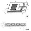
- FIG. 1 shows, in a three-dimensional representation, a single strain gage 13 arranged on a support 15, which has a strain-dependent resistance path 14, which is preferably meander-shaped on a support 15, and connection electrodes 17, and which is provided with a multilayer layer 16.
- the multi-layer 16 is drawn transparent and broken.
- It consists of a regular sequence of polymer layers 19 ', 19 ", 19”', preferably of a polyacrylate or polymethacrylate, and barrier layers 20, of a predominantly inorganic insulator, wherein the polymer layers 19 ', 19 ", 19”' have a thickness of typically 50 to 500 nm, preferably 100 nm to 200 nm, in individual cases but also beyond a layer thickness of up to 1500 nm may have.
- the layer thickness of the barrier layers 20 is typically between 5 nm and 200 nm, preferably between 10 nm and 50 nm, and in individual cases can also be up to 500 nm.
- the side edges of the carrier 15 are not shown covered in the figure 1 of the multi-layer layer.
- FIG. 2 shows a section through a strain gauge 13 with an applied multilayer layer 16 consisting of a total of five thin individual layers.
- the drawing is highly schematic and it is the respective thickness of the carrier 15, the resistor track 14 and the barrier layers 20 and the polymer layers 19 ', 19 ", 19"' drawn here not to scale.
- the first layer 19 'of the multilayer 16 directly adjacent to the carrier 15 and in the regions of the resistive track 14 applied to the carrier 15, the latter contacting the carrier and resistor tracks is preferably an acrylate polymer layer which serves to increase the roughnesses of the carrier 15 and resistor track 14 smooth. It may possibly have a greater thickness than the other polymeric intermediate layers 19 "of the multi-layer layer 16. With such acrylate polymer layers, the roughness of a substrate in the nanometer range can be smoothed out in that the formation of pinholes in the first barrier layer 20 is reduced by the smoothing effect of its backing.
- Another reason for making the first polymer layer 19 'of the multilayered layer 16 somewhat thicker compared to the remaining polymer layers 19 ", 19"' is that there is a requirement to completely cover the lateral edges of the resistance path 14.
- Said polymer layer fulfills this requirement by virtue of its properties on the one hand on a nanometer scale and on the other hand its properties covering on the micrometer scale both to a certain extent and covering the surfaces extending predominantly perpendicular to the layer plane. Thus, it creates the prerequisite for the formation of uniformly thick and defect-poor barrier layers 20 and subsequent layers of the multilayer 16.
- the first barrier layer 20 is followed by a polymeric interlayer. Their function is not only to stabilize the first barrier layer 20, but also to reduce the formation of pinholes in a further barrier layer 20 following the intermediate layer 19 ", but in particular the interlayer 19 avoids the fact that it is nevertheless produced in small numbers Pinholes a second barrier layer 20 to be fixed to those of the first barrier layer 20, which would favor the passage of moisture again.
- Much more caused by the independent localization of Pinholes in the first and in the second barrier layer 20 is a kind of labyrinth for penetrating moisture, especially water or solvent molecules. This labyrinth effect results in a drastic reduction of penetrating moisture in a multilayer coating with successive barrier layers 20 and polymer layers 19 ', 19 ", 19'".
- the multi-layer layer 16 shown in FIG. 2 has five thin individual layers, of which the first layer is the ausbnende polymer layer 19 'and the boundary layer to the ambient atmosphere forming layer is again a polymer layer 19 "' to the multi-layer 16 especially against mechanical damage
- the multilayer layer 16 may have further individual layers, and the sequence of the polymer layer 19 "and the barrier layer 20 may in principle be repeated as often as desired.
- the multilayer layer 16 may also consist of a total of only three thin individual layers, preferably of a sequence of polymer layer 19 '- barrier layer 20 - polymer layer 19 "'.
- the barrier layers 20 As materials for the barrier layers 20, a variety of known, applicable in various coating methods mainly inorganic insulators can be used. Examples which may be mentioned here oxides, nitrides, fluorides, carbides, borides or combinations thereof, in particular oxi-nitrides, or mixed ceramics. In particular, silicon oxide, titanium oxide, chromium oxide, aluminum oxide, silicon nitride and titanium nitride have proved to be the material for the barrier layers 20. The so-called diamond-like carbon layers can also be used as possible barrier layers.
- Metals for example silver, aluminum, gold, chromium, copper, nickel, titanium and alloys, for example nickel-cobalt alloys, or intermetallic compounds, for example of aluminum and copper, of tungsten are also used as further materials for the barrier layers 20 and copper or of titanium and aluminum in question.
- polymers Amides, alkyds, styrenes, xylylene, phenylenes, aldehydes, esters, urethanes, epoxides, imides, phenols, ketones, and fluoropolymers or copolymers, but the list may not be exhaustive.
- the optimization between barrier effect, combinability of the barrier layer 20 and the polymer layer 19 ', 19 ", 19"' and cost effectiveness of the coating method decide on the use of the barrier layer material as well as on the use of the polymer material.
- ORMOCER Another class of materials that can be used as polymeric intermediate layers 19 "or polymer covering layer 19 '' 'are inorganic-organic hybrid polymers with the trade name" ORMOCER. "These materials are described in DE 38 28 098 A1 and DE 43 03 570 A1 Although the barrier effect is not high enough that it would be suitable for use as a barrier layer 20, a particular advantage of ORMOCER is that these materials can be deposited in air For example, by spray, spin or pad printing.
- a thin barrier layer 20 has a correspondingly low rigidity. Therefore, in conjunction with the per se flexible polymer layer 19 ', 19 ", 19"' only a minimal force shunt by the application of a multi-layer 16 with ultrathin barrier layers 20 on strain gauges 13 to be feared. For the same reason, the risk of detachment of the ultra-thin barrier layers 20 from their delamination has been massively reduced and could not be observed for materials used in the invention.
- strain gauges 13 with a multi-layer 16 following the preparation of the strain gauges 13 takes place, as long as they are still present in a series or surface arrangement, remain at a separation of the strain gauges 13, however, the side surfaces, in particular the carrier film, open and penetrating Moisture accessible. Due to the area ratios of top and side edges of a strain gauge, however, the protective effect of the inventive multi-layer 16 is still quite high. Strain gauges can be used with this extremely efficient coating method 13, whose moisture absorption, depending on the materials used by a factor of 50 to 1000 is smaller, compared to uncoated strain gauges. In the event that a higher barrier effect than that mentioned would have to be achieved, it is of course also possible to coat individual strain gauges 13, possibly completely, whereby the side surfaces of the carrier 15 would be covered, at least with careful handling.
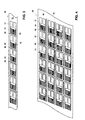
- FIG. 3 shows a series arrangement 30 of strain gauges 13.
- the carrier 31 of the series arrangement 30 is interrupted by narrow slits 32 oriented transversely to the longitudinal extent of the series arrangement 30, wherein the slits 32 do not extend beyond the slits 32 entire width of the carrier 31 of the array 30 range.
- the slits 32 may be formed after application of the resistive track 14 and the terminal electrodes 17 by various methods such as water cutting, laser cutting or, preferably, stamping in the carrier 31 as well.
- FIG. 4 shows a surface arrangement 35 of strain gauges 13 in which slots 32 and slots 34 arranged perpendicularly to each other in the regions between the individual resistance electrodes 14 connected to their respective connection electrodes 17 break through the support 36 of the surface arrangement 35 so that it only adjoins four Connecting points 37 is connected to each strain gauge 13.
- the slits 32, 34 are produced at those points of a carrier, to which at a later separation of the strain gauges 13, these from the Surface arrangement 35 are separated out.
- such a slit arrangement can be varied in many ways, for example, such that the slits make a right angle around the resistive paths 14 connected to their respective terminal electrodes 17, and are interconnected only at two or three junctions of the support 36.
- the strain gauges can be linked together at more than four joints with each other.
- connection points 33, 37 It is important to minimize the connection of the carrier 31, 36 at the connection points 33, 37, that is to keep the surface of the connection points 33, 37 so small that, on the one hand, the edges of a strain gauge 13 are covered by the protective layer in as large a range as possible can, on the other hand, but for the handling of the array 30 or surface arrangement 35 of strain gauges 13 still a sufficiently high cohesion of the carrier 31, 36 is present. It has been found that in this way it was possible to reduce the penetration of moisture into strain gauges from a series or surface arrangement of the prior art and to sustainably improve the sensitivity of a load cell subjected to such strain gauges.
- the width of a slit 32, 37 should be selected such that on the one hand not too much carrier material is lost between the individual strain gauges 13 and on the other hand the coating materials to be applied ensure sufficient coverage of the side edges of a strain gage 13.
- a width of about 0.5 mm is mentioned here as an orientation value.
- the individual barrier layers 20 are not necessarily of the same material. Nor are the polymer layers 19 ', 19 ", 19"' limited to a single material.
- the multi-layer 16 is composed of an alternating sequence of a polymer layer 19 ', 19 ", 19"', in particular a polyacrylate or polymethacrylate layer and a barrier layer 20, preferably of silicon oxide or aluminum oxide, due to the choice an efficient coating process, the materials used are uniform, as well as well as the individual layers are homogeneous in themselves.
- the boundary layer to the carrier 15 or to the resistance path 14 and the connection electrodes 17 is a polymer layer 19 ', for the boundary layer to the ambient atmosphere, this is not absolutely necessary, although preferred, since a final polymer layer 19 "' good mechanical and optionally chemical protection for a last This means that, if appropriate, the choice of the polymer material used for the final polymer layer 19 "'is carried out with regard to the property of being able to provide particularly good mechanical and / or chemical protection.
- the preferred method of forming a multilayer 16 on a series array of strain gauges 13 includes the steps of depositing a nanometer scale polymer layer 19 'having a thickness that is between 200 nm and 1500 nm, depositing an approximately 20 nm thick barrier layer 20 on the polymer layer 19 ', deposition of a further thin polymer layer 19 "with a thickness of about 100 nm to 200 nm on the barrier layer 20, any repetition of the process of coating with a barrier layer 20 and a polymer layer 19", where as a boundary layer to the ambient atmosphere a polymer layer 19 "'or a thin barrier layer 20 may be present.
- the substrate of the multi-layer layer 16 be it the substrate 15, 31, 36, to a carrier foil or the resistance track 14 for plasma cleaning or chemical cleaning.
- vapor deposition in vacuo vapor deposition in air
- plasma coating can be used here for producing the barrier layers 20.
- plasma coating "sputtering”, sol-gel process, “chemical vapor deposition (CVD)”, “combustion chemical vapor deposition (CCVD)”, “plasma enhanced chemical vapor deposition (PECVD)”, “plasma impulse chemical vapor deposition (PICVD)”
- CVD chemical vapor deposition
- CCVD combustion chemical vapor deposition
- PECVD plasma enhanced chemical vapor deposition
- PICVD plasma impulse chemical vapor deposition
- the following coating methods are possible for applying the polymer layers: vapor deposition in vacuo, evaporation in air, in situ polymerization of monomers or oligomers applied by flash evaporation or plasma coating, and electrophoresis, cataphoresis or anaphoresis.
- a method for coating strain gauges 13, which can be applied to the deformation body of a load cell, has proved to be particularly efficient when the multilayer coating 16 is produced by alternating coating with polymer layers 19 ', 19 ", 19"' and barrier layers 20 within a coating apparatus done by two sources in one operation.
Priority Applications (1)
| Application Number | Priority Date | Filing Date | Title |
|---|---|---|---|
| EP05109509A EP1686356B1 (fr) | 2002-07-25 | 2003-07-22 | Protection contre l'humidité pour un transducteur électromécanique |
Applications Claiming Priority (3)
| Application Number | Priority Date | Filing Date | Title |
|---|---|---|---|
| EP02102061A EP1384980A1 (fr) | 2002-07-25 | 2002-07-25 | Protection contre l'humidité pour un transducteur électromécanique |
| EP05109509A EP1686356B1 (fr) | 2002-07-25 | 2003-07-22 | Protection contre l'humidité pour un transducteur électromécanique |
| EP03771117A EP1535035B1 (fr) | 2002-07-25 | 2003-07-22 | Systeme de protection contre l'humidite pour un transducteur electromecanique |
Related Parent Applications (2)
| Application Number | Title | Priority Date | Filing Date |
|---|---|---|---|
| EP03771117A Division EP1535035B1 (fr) | 2002-07-25 | 2003-07-22 | Systeme de protection contre l'humidite pour un transducteur electromecanique |
| EP03771117.3 Division | 2003-07-22 |
Publications (3)
| Publication Number | Publication Date |
|---|---|
| EP1686356A2 true EP1686356A2 (fr) | 2006-08-02 |
| EP1686356A3 EP1686356A3 (fr) | 2006-08-09 |
| EP1686356B1 EP1686356B1 (fr) | 2011-12-07 |
Family
ID=29797288
Family Applications (3)
| Application Number | Title | Priority Date | Filing Date |
|---|---|---|---|
| EP02102061A Withdrawn EP1384980A1 (fr) | 2002-07-25 | 2002-07-25 | Protection contre l'humidité pour un transducteur électromécanique |
| EP05109509A Expired - Lifetime EP1686356B1 (fr) | 2002-07-25 | 2003-07-22 | Protection contre l'humidité pour un transducteur électromécanique |
| EP03771117A Expired - Lifetime EP1535035B1 (fr) | 2002-07-25 | 2003-07-22 | Systeme de protection contre l'humidite pour un transducteur electromecanique |
Family Applications Before (1)
| Application Number | Title | Priority Date | Filing Date |
|---|---|---|---|
| EP02102061A Withdrawn EP1384980A1 (fr) | 2002-07-25 | 2002-07-25 | Protection contre l'humidité pour un transducteur électromécanique |
Family Applications After (1)
| Application Number | Title | Priority Date | Filing Date |
|---|---|---|---|
| EP03771117A Expired - Lifetime EP1535035B1 (fr) | 2002-07-25 | 2003-07-22 | Systeme de protection contre l'humidite pour un transducteur electromecanique |
Country Status (9)
| Country | Link |
|---|---|
| US (1) | US7197940B2 (fr) |
| EP (3) | EP1384980A1 (fr) |
| JP (1) | JP2005534020A (fr) |
| CN (1) | CN100588924C (fr) |
| AT (2) | ATE536538T1 (fr) |
| AU (1) | AU2003262533A1 (fr) |
| DE (1) | DE50312534D1 (fr) |
| DK (1) | DK1535035T3 (fr) |
| WO (1) | WO2004011892A1 (fr) |
Cited By (3)
| Publication number | Priority date | Publication date | Assignee | Title |
|---|---|---|---|---|
| EP1560011B1 (fr) * | 2004-01-27 | 2010-03-17 | Mettler-Toledo AG | Jauge de contrainte avec protection contre l'humidité au moyen d'une couche inorganique inhomogène sur une couche polymère d'égalisation (ORMOCER) et un arrangement de fentes |
| FR2937727A1 (fr) * | 2008-10-24 | 2010-04-30 | Snecma | Procede pour installer et proteger un capteur sur un substrat |
| FR2937726A1 (fr) * | 2008-10-24 | 2010-04-30 | Snecma | Procede pour installer et proteger un capteur sur un substrat |
Families Citing this family (34)
| Publication number | Priority date | Publication date | Assignee | Title |
|---|---|---|---|---|
| US20070062300A1 (en) * | 2003-09-25 | 2007-03-22 | Dorfman Benjamin F | Method and apparatus for straining-stress sensors and smart skin for air craft and space vehicles |
| DE102005012686A1 (de) * | 2005-01-14 | 2006-07-27 | Trafag Ag | Drucksensor, darin verwendbarer Verformungskörper und Herstellverfahren dafür |
| US8173995B2 (en) | 2005-12-23 | 2012-05-08 | E. I. Du Pont De Nemours And Company | Electronic device including an organic active layer and process for forming the electronic device |
| US8033156B2 (en) * | 2008-06-25 | 2011-10-11 | The Boeing Company | Sensor apparatus and method for detecting impacts |
| US7945388B2 (en) * | 2008-06-25 | 2011-05-17 | The Boeing Company | Test bed for in-situ studies |
| TWI348716B (en) * | 2008-08-13 | 2011-09-11 | Cyntec Co Ltd | Resistive component and making method thereof |
| JP2010169616A (ja) * | 2009-01-26 | 2010-08-05 | A & D Co Ltd | 歪ゲージとロードセル。 |
| JP5713615B2 (ja) * | 2010-09-17 | 2015-05-07 | 大和製衡株式会社 | ロードセル |
| DE102012210021A1 (de) * | 2012-06-14 | 2013-12-19 | Tecsis Gmbh | Kraftsensor mit einer Sensorplatte mit lokalen Unterschieden der Steifigkeit |
| CN102735378B (zh) * | 2012-06-21 | 2014-07-02 | 戴文钟 | 压力传感器 |
| CN102998049A (zh) * | 2012-11-28 | 2013-03-27 | 安徽埃克森科技集团有限公司 | 一种防腐蚀压阻式压力传感器 |
| JP5973357B2 (ja) * | 2013-02-05 | 2016-08-23 | 株式会社鷺宮製作所 | 圧力検知ユニット及び圧力検知ユニットの製造方法 |
| JP6259967B2 (ja) * | 2014-01-30 | 2018-01-17 | 地方独立行政法人大阪産業技術研究所 | 歪抵抗薄膜およびこれを用いた歪センサ素子 |
| DE102014103065A1 (de) * | 2014-03-07 | 2015-09-10 | Leifheit Ag | Küchenwaage |
| CN104075654A (zh) * | 2014-04-10 | 2014-10-01 | 中北大学 | 一种高速小目标侵彻明胶体的应变量测试系统 |
| CN104075653A (zh) * | 2014-04-10 | 2014-10-01 | 中北大学 | 一种基于正交应变片阵列的应变量测试系统 |
| CN104062048B (zh) * | 2014-05-15 | 2016-06-29 | 浙江工业大学 | 高压氢环境下的载荷传感器 |
| CN104062047B (zh) * | 2014-05-15 | 2016-05-11 | 浙江工业大学 | 高压硫化氢环境用电阻应变式载荷传感器 |
| GB2528897A (en) * | 2014-08-03 | 2016-02-10 | Shekel Scales Co 2008 Ltd | Low-profile load cell assembly |
| JP2015096868A (ja) * | 2015-01-20 | 2015-05-21 | 大和製衡株式会社 | ロードセル |
| DE202015104676U1 (de) | 2015-09-03 | 2015-11-23 | Leifheit Ag | Küchenwaage |
| CN105222701A (zh) * | 2015-10-22 | 2016-01-06 | 桂林电子科技大学 | 一种具有耐酸碱腐蚀性能的应变式传感器 |
| CN105220198B (zh) * | 2015-10-22 | 2017-12-19 | 桂林电子科技大学 | 一种耐酸碱腐蚀轻金属材料弹性体及其制造工艺 |
| JP2019078726A (ja) * | 2017-10-27 | 2019-05-23 | ミネベアミツミ株式会社 | ひずみゲージ、センサモジュール |
| JP2019082425A (ja) * | 2017-10-31 | 2019-05-30 | ミネベアミツミ株式会社 | ひずみゲージ |
| JP2019120555A (ja) * | 2017-12-28 | 2019-07-22 | ミネベアミツミ株式会社 | ひずみゲージ、センサモジュール |
| JP2019174387A (ja) | 2018-03-29 | 2019-10-10 | ミネベアミツミ株式会社 | ひずみゲージ |
| JP2019184284A (ja) * | 2018-04-03 | 2019-10-24 | ミネベアミツミ株式会社 | ひずみゲージ |
| CN110873616A (zh) * | 2018-08-31 | 2020-03-10 | 梅特勒-托利多(常州)精密仪器有限公司 | 防潮应变片及其制备方法 |
| EP3617683A1 (fr) * | 2018-08-31 | 2020-03-04 | Mettler Toledo (Changzhou) Precision Instrument Ltd. | Procédé d'isolation d'un détecteur de contrainte contre la pénétration d'humidité |
| CN109702556B (zh) * | 2019-01-29 | 2023-07-14 | 孝感松林智能计测器有限公司 | 一种不平衡校正去重刀具的对刀系统及其使用方法 |
| JP7426794B2 (ja) * | 2019-10-01 | 2024-02-02 | ミネベアミツミ株式会社 | センサモジュール |
| CN111162018B (zh) * | 2019-12-24 | 2023-06-06 | 陕西电器研究所 | 一种等离子体刻蚀调整薄膜传感器零位的方法 |
| JP2022086254A (ja) * | 2020-11-30 | 2022-06-09 | 株式会社イシダ | 歪みゲージ及び歪みゲージの製造方法 |
Citations (1)
| Publication number | Priority date | Publication date | Assignee | Title |
|---|---|---|---|---|
| JPH07113697A (ja) | 1993-10-19 | 1995-05-02 | Tec Corp | ロードセル |
Family Cites Families (12)
| Publication number | Priority date | Publication date | Assignee | Title |
|---|---|---|---|---|
| DE2728916A1 (de) * | 1977-06-27 | 1979-01-18 | Hottinger Messtechnik Baldwin | Verfahren und vorrichtung zum abdecken eines dehnungsmesstreifens |
| US4185496A (en) * | 1978-08-28 | 1980-01-29 | Gould Inc. | Thin film strain gage and process therefor |
| AU547838B2 (en) * | 1982-10-26 | 1985-11-07 | Ishida Koki Seisakusho K.K. | Load cell |
| GB8303555D0 (en) * | 1983-02-09 | 1983-03-16 | Strain Measurement Dev Ltd | Strain gauges |
| JPH01212327A (ja) * | 1988-02-19 | 1989-08-25 | Ishida Scales Mfg Co Ltd | ロードセルおよびその製造方法 |
| DE3828098A1 (de) | 1988-08-18 | 1990-03-08 | Fraunhofer Ges Forschung | Verfahren und zusammensetzung zur herstellung von kratzfesten materialien |
| SU1709724A1 (ru) * | 1989-09-29 | 1995-09-10 | Научно-производственное объединение "Полимерклей" | Липкая лента |
| DE4015666A1 (de) | 1990-05-16 | 1991-11-28 | Deutsche Forsch Luft Raumfahrt | Kraftaufnehmer |
| US5289722A (en) * | 1992-04-27 | 1994-03-01 | Kansas State University Research Foundation | Preassembled, easily mountable strain gage |
| DE4303570C2 (de) | 1993-02-08 | 1997-03-20 | Fraunhofer Ges Forschung | Verfahren zur Herstellung von funktionellen Beschichtungen, beschichtete Substrate und Beschichtungsmaterial |
| DE4404716A1 (de) * | 1994-02-15 | 1995-08-17 | Hottinger Messtechnik Baldwin | Dehnungsmeßstreifen und Verfahren zur Herstellung eines Dehnungsmeßstreifens sowie Meßgrößenaufnehmer |
| US5616227A (en) | 1995-06-26 | 1997-04-01 | Dionex Corporation | Method for extending the life of electrophoretic gels |
-
2002
- 2002-07-25 EP EP02102061A patent/EP1384980A1/fr not_active Withdrawn
-
2003
- 2003-07-22 DK DK03771117.3T patent/DK1535035T3/da active
- 2003-07-22 AT AT05109509T patent/ATE536538T1/de active
- 2003-07-22 CN CN03817789A patent/CN100588924C/zh not_active Expired - Lifetime
- 2003-07-22 AT AT03771117T patent/ATE461436T1/de not_active IP Right Cessation
- 2003-07-22 DE DE50312534T patent/DE50312534D1/de not_active Expired - Lifetime
- 2003-07-22 EP EP05109509A patent/EP1686356B1/fr not_active Expired - Lifetime
- 2003-07-22 EP EP03771117A patent/EP1535035B1/fr not_active Expired - Lifetime
- 2003-07-22 WO PCT/EP2003/050326 patent/WO2004011892A1/fr active Application Filing
- 2003-07-22 AU AU2003262533A patent/AU2003262533A1/en not_active Abandoned
- 2003-07-22 JP JP2004523814A patent/JP2005534020A/ja active Pending
-
2005
- 2005-01-24 US US11/040,015 patent/US7197940B2/en not_active Expired - Lifetime
Patent Citations (1)
| Publication number | Priority date | Publication date | Assignee | Title |
|---|---|---|---|---|
| JPH07113697A (ja) | 1993-10-19 | 1995-05-02 | Tec Corp | ロードセル |
Cited By (3)
| Publication number | Priority date | Publication date | Assignee | Title |
|---|---|---|---|---|
| EP1560011B1 (fr) * | 2004-01-27 | 2010-03-17 | Mettler-Toledo AG | Jauge de contrainte avec protection contre l'humidité au moyen d'une couche inorganique inhomogène sur une couche polymère d'égalisation (ORMOCER) et un arrangement de fentes |
| FR2937727A1 (fr) * | 2008-10-24 | 2010-04-30 | Snecma | Procede pour installer et proteger un capteur sur un substrat |
| FR2937726A1 (fr) * | 2008-10-24 | 2010-04-30 | Snecma | Procede pour installer et proteger un capteur sur un substrat |
Also Published As
| Publication number | Publication date |
|---|---|
| ATE536538T1 (de) | 2011-12-15 |
| EP1535035A1 (fr) | 2005-06-01 |
| CN1672022A (zh) | 2005-09-21 |
| DE50312534D1 (de) | 2010-04-29 |
| EP1535035B1 (fr) | 2010-03-17 |
| US7197940B2 (en) | 2007-04-03 |
| ATE461436T1 (de) | 2010-04-15 |
| CN100588924C (zh) | 2010-02-10 |
| AU2003262533A1 (en) | 2004-02-16 |
| WO2004011892A1 (fr) | 2004-02-05 |
| EP1686356B1 (fr) | 2011-12-07 |
| EP1384980A1 (fr) | 2004-01-28 |
| JP2005534020A (ja) | 2005-11-10 |
| EP1686356A3 (fr) | 2006-08-09 |
| US20050155435A1 (en) | 2005-07-21 |
| DK1535035T3 (da) | 2010-07-12 |
Similar Documents
| Publication | Publication Date | Title |
|---|---|---|
| EP1686356B1 (fr) | Protection contre l'humidité pour un transducteur électromécanique | |
| EP1560011B1 (fr) | Jauge de contrainte avec protection contre l'humidité au moyen d'une couche inorganique inhomogène sur une couche polymère d'égalisation (ORMOCER) et un arrangement de fentes | |
| EP0667514B1 (fr) | Jauge de contrainte et méthode de sa fabrication | |
| EP0019135B1 (fr) | Sonde pour l'application à la mesure de la température ou de la masse d'un milieu en écoulement et procédé pour sa fabrication | |
| DE4023778C2 (de) | Kapazitiver Feuchtigkeitssensor und Verfahren zur Herstellung des Sensors | |
| WO2001042776A1 (fr) | Capteur capacitif | |
| EP1144968B1 (fr) | Thermometre a resistance de platine et son procede de production | |
| DE102016108985A1 (de) | Verfahren zur Herstellung eines Sensorelements mittels Laserstrukturierung | |
| EP0191785A1 (fr) | Procede de fabrication d'une sonde de mesure destinee a la mesure de la temperature ou de la masse d'un fluide en ecoulement | |
| EP0017982B1 (fr) | Jauge de contrainte et sa fabrication | |
| EP0460249B1 (fr) | Jauge de contrainte | |
| EP0278021B1 (fr) | Jauges de contrainte à résistance avec une couche mince métallique discontinue | |
| DE102010054970B4 (de) | Vorrichtung zum Wandeln einer Dehnung und/oder Stauchung in ein elektrisches Signal, insbesondere Dehnungsmessfolie | |
| DE602004010927T2 (de) | Mikroelektromechanische hochfrequenz-systeme und verfahren zur herstellung solcher systeme | |
| DE102016217585B3 (de) | Dehnungsmesstreifen sowie Verfahren zur Herstellung eines Dehnungsmessstreifens | |
| WO2011160794A1 (fr) | Capteur de force piézo-résistif | |
| EP0992778A2 (fr) | Capteur et son procédé de fabricage | |
| WO2012010301A1 (fr) | Jauge de contrainte | |
| WO2007062813A1 (fr) | Ruban de mesure d'allongement | |
| EP0058835B1 (fr) | Dispositif à semiconducteur et procédé pour sa fabrication | |
| EP0235329B1 (fr) | Lame de mesure munie d'un assemblage de jauges de contraintes à couches minces et son procédé de fabrication | |
| DE102018211332A1 (de) | Verfahren zur Herstellung eines MEMS-Sensors sowie MEMS-Sensor | |
| DE102018209503A1 (de) | Verfahren zur Herstellung eines MEMS-Drucksensors | |
| DE102006010857A1 (de) | Dehnungsmessstreifen | |
| DE102013107271A1 (de) | Sensor zur Erfassung druckabhängiger Messwerte in Dünnschichtbauweise |
Legal Events
| Date | Code | Title | Description |
|---|---|---|---|
| PUAI | Public reference made under article 153(3) epc to a published international application that has entered the european phase |
Free format text: ORIGINAL CODE: 0009012 |
|
| PUAL | Search report despatched |
Free format text: ORIGINAL CODE: 0009013 |
|
| AC | Divisional application: reference to earlier application |
Ref document number: 1535035 Country of ref document: EP Kind code of ref document: P |
|
| AK | Designated contracting states |
Kind code of ref document: A2 Designated state(s): AT BE BG CH CY CZ DE DK EE ES FI FR GB GR HU IE IT LI LU MC NL PT RO SE SI SK TR |
|
| AK | Designated contracting states |
Kind code of ref document: A3 Designated state(s): AT BE BG CH CY CZ DE DK EE ES FI FR GB GR HU IE IT LI LU MC NL PT RO SE SI SK TR |
|
| RIC1 | Information provided on ipc code assigned before grant |
Ipc: G01B 7/16 20060101ALI20060705BHEP Ipc: G01G 3/14 20060101ALI20060705BHEP Ipc: G01L 1/22 20060101AFI20060705BHEP |
|
| RAP1 | Party data changed (applicant data changed or rights of an application transferred) |
Owner name: METTLER-TOLEDO AG |
|
| 17P | Request for examination filed |
Effective date: 20070130 |
|
| 17Q | First examination report despatched |
Effective date: 20070306 |
|
| AKX | Designation fees paid |
Designated state(s): AT BE BG CH CY CZ DE DK EE ES FI FR GB GR HU IE IT LI LU MC NL PT RO SE SI SK TR |
|
| GRAP | Despatch of communication of intention to grant a patent |
Free format text: ORIGINAL CODE: EPIDOSNIGR1 |
|
| GRAS | Grant fee paid |
Free format text: ORIGINAL CODE: EPIDOSNIGR3 |
|
| GRAA | (expected) grant |
Free format text: ORIGINAL CODE: 0009210 |
|
| AC | Divisional application: reference to earlier application |
Ref document number: 1535035 Country of ref document: EP Kind code of ref document: P |
|
| AK | Designated contracting states |
Kind code of ref document: B1 Designated state(s): AT BE BG CH CY CZ DE DK EE ES FI FR GB GR HU IE IT LI LU MC NL PT RO SE SI SK TR |
|
| REG | Reference to a national code |
Ref country code: GB Ref legal event code: FG4D Free format text: NOT ENGLISH |
|
| REG | Reference to a national code |
Ref country code: CH Ref legal event code: EP |
|
| REG | Reference to a national code |
Ref country code: IE Ref legal event code: FG4D Free format text: LANGUAGE OF EP DOCUMENT: GERMAN |
|
| REG | Reference to a national code |
Ref country code: DE Ref legal event code: R081 Ref document number: 50314112 Country of ref document: DE Owner name: METTLER-TOLEDO GMBH, CH Free format text: FORMER OWNER: METTLER-TOLEDO GMBH, GREIFENSEE, CH |
|
| REG | Reference to a national code |
Ref country code: DE Ref legal event code: R096 Ref document number: 50314112 Country of ref document: DE Effective date: 20120308 |
|
| REG | Reference to a national code |
Ref country code: NL Ref legal event code: VDEP Effective date: 20111207 |
|
| PG25 | Lapsed in a contracting state [announced via postgrant information from national office to epo] |
Ref country code: SE Free format text: LAPSE BECAUSE OF FAILURE TO SUBMIT A TRANSLATION OF THE DESCRIPTION OR TO PAY THE FEE WITHIN THE PRESCRIBED TIME-LIMIT Effective date: 20111207 Ref country code: GR Free format text: LAPSE BECAUSE OF FAILURE TO SUBMIT A TRANSLATION OF THE DESCRIPTION OR TO PAY THE FEE WITHIN THE PRESCRIBED TIME-LIMIT Effective date: 20120308 Ref country code: SI Free format text: LAPSE BECAUSE OF FAILURE TO SUBMIT A TRANSLATION OF THE DESCRIPTION OR TO PAY THE FEE WITHIN THE PRESCRIBED TIME-LIMIT Effective date: 20111207 Ref country code: NL Free format text: LAPSE BECAUSE OF FAILURE TO SUBMIT A TRANSLATION OF THE DESCRIPTION OR TO PAY THE FEE WITHIN THE PRESCRIBED TIME-LIMIT Effective date: 20111207 |
|
| PG25 | Lapsed in a contracting state [announced via postgrant information from national office to epo] |
Ref country code: CY Free format text: LAPSE BECAUSE OF FAILURE TO SUBMIT A TRANSLATION OF THE DESCRIPTION OR TO PAY THE FEE WITHIN THE PRESCRIBED TIME-LIMIT Effective date: 20111207 |
|
| REG | Reference to a national code |
Ref country code: IE Ref legal event code: FD4D |
|
| PG25 | Lapsed in a contracting state [announced via postgrant information from national office to epo] |
Ref country code: BG Free format text: LAPSE BECAUSE OF FAILURE TO SUBMIT A TRANSLATION OF THE DESCRIPTION OR TO PAY THE FEE WITHIN THE PRESCRIBED TIME-LIMIT Effective date: 20120307 Ref country code: SK Free format text: LAPSE BECAUSE OF FAILURE TO SUBMIT A TRANSLATION OF THE DESCRIPTION OR TO PAY THE FEE WITHIN THE PRESCRIBED TIME-LIMIT Effective date: 20111207 Ref country code: CZ Free format text: LAPSE BECAUSE OF FAILURE TO SUBMIT A TRANSLATION OF THE DESCRIPTION OR TO PAY THE FEE WITHIN THE PRESCRIBED TIME-LIMIT Effective date: 20111207 Ref country code: IE Free format text: LAPSE BECAUSE OF FAILURE TO SUBMIT A TRANSLATION OF THE DESCRIPTION OR TO PAY THE FEE WITHIN THE PRESCRIBED TIME-LIMIT Effective date: 20111207 Ref country code: EE Free format text: LAPSE BECAUSE OF FAILURE TO SUBMIT A TRANSLATION OF THE DESCRIPTION OR TO PAY THE FEE WITHIN THE PRESCRIBED TIME-LIMIT Effective date: 20111207 |
|
| PG25 | Lapsed in a contracting state [announced via postgrant information from national office to epo] |
Ref country code: RO Free format text: LAPSE BECAUSE OF FAILURE TO SUBMIT A TRANSLATION OF THE DESCRIPTION OR TO PAY THE FEE WITHIN THE PRESCRIBED TIME-LIMIT Effective date: 20111207 Ref country code: PT Free format text: LAPSE BECAUSE OF FAILURE TO SUBMIT A TRANSLATION OF THE DESCRIPTION OR TO PAY THE FEE WITHIN THE PRESCRIBED TIME-LIMIT Effective date: 20120409 |
|
| PLBE | No opposition filed within time limit |
Free format text: ORIGINAL CODE: 0009261 |
|
| STAA | Information on the status of an ep patent application or granted ep patent |
Free format text: STATUS: NO OPPOSITION FILED WITHIN TIME LIMIT |
|
| PG25 | Lapsed in a contracting state [announced via postgrant information from national office to epo] |
Ref country code: DK Free format text: LAPSE BECAUSE OF FAILURE TO SUBMIT A TRANSLATION OF THE DESCRIPTION OR TO PAY THE FEE WITHIN THE PRESCRIBED TIME-LIMIT Effective date: 20111207 |
|
| 26N | No opposition filed |
Effective date: 20120910 |
|
| PG25 | Lapsed in a contracting state [announced via postgrant information from national office to epo] |
Ref country code: IT Free format text: LAPSE BECAUSE OF FAILURE TO SUBMIT A TRANSLATION OF THE DESCRIPTION OR TO PAY THE FEE WITHIN THE PRESCRIBED TIME-LIMIT Effective date: 20111207 |
|
| REG | Reference to a national code |
Ref country code: DE Ref legal event code: R097 Ref document number: 50314112 Country of ref document: DE Effective date: 20120910 |
|
| BERE | Be: lapsed |
Owner name: METTLER-TOLEDO A.G. Effective date: 20120731 |
|
| PG25 | Lapsed in a contracting state [announced via postgrant information from national office to epo] |
Ref country code: MC Free format text: LAPSE BECAUSE OF NON-PAYMENT OF DUE FEES Effective date: 20120731 |
|
| PG25 | Lapsed in a contracting state [announced via postgrant information from national office to epo] |
Ref country code: ES Free format text: LAPSE BECAUSE OF FAILURE TO SUBMIT A TRANSLATION OF THE DESCRIPTION OR TO PAY THE FEE WITHIN THE PRESCRIBED TIME-LIMIT Effective date: 20120318 |
|
| PG25 | Lapsed in a contracting state [announced via postgrant information from national office to epo] |
Ref country code: BE Free format text: LAPSE BECAUSE OF NON-PAYMENT OF DUE FEES Effective date: 20120731 |
|
| PG25 | Lapsed in a contracting state [announced via postgrant information from national office to epo] |
Ref country code: FI Free format text: LAPSE BECAUSE OF FAILURE TO SUBMIT A TRANSLATION OF THE DESCRIPTION OR TO PAY THE FEE WITHIN THE PRESCRIBED TIME-LIMIT Effective date: 20111207 |
|
| REG | Reference to a national code |
Ref country code: AT Ref legal event code: MM01 Ref document number: 536538 Country of ref document: AT Kind code of ref document: T Effective date: 20120731 |
|
| PG25 | Lapsed in a contracting state [announced via postgrant information from national office to epo] |
Ref country code: AT Free format text: LAPSE BECAUSE OF NON-PAYMENT OF DUE FEES Effective date: 20120731 |
|
| REG | Reference to a national code |
Ref country code: CH Ref legal event code: PCOW Free format text: NEW ADDRESS: IM LANGACHER 44, 8606 GREIFENSEE (CH) |
|
| PG25 | Lapsed in a contracting state [announced via postgrant information from national office to epo] |
Ref country code: TR Free format text: LAPSE BECAUSE OF FAILURE TO SUBMIT A TRANSLATION OF THE DESCRIPTION OR TO PAY THE FEE WITHIN THE PRESCRIBED TIME-LIMIT Effective date: 20111207 |
|
| PG25 | Lapsed in a contracting state [announced via postgrant information from national office to epo] |
Ref country code: LU Free format text: LAPSE BECAUSE OF NON-PAYMENT OF DUE FEES Effective date: 20120722 |
|
| PG25 | Lapsed in a contracting state [announced via postgrant information from national office to epo] |
Ref country code: HU Free format text: LAPSE BECAUSE OF FAILURE TO SUBMIT A TRANSLATION OF THE DESCRIPTION OR TO PAY THE FEE WITHIN THE PRESCRIBED TIME-LIMIT Effective date: 20030722 |
|
| PGFP | Annual fee paid to national office [announced via postgrant information from national office to epo] |
Ref country code: GB Payment date: 20140624 Year of fee payment: 12 |
|
| PGFP | Annual fee paid to national office [announced via postgrant information from national office to epo] |
Ref country code: CH Payment date: 20140725 Year of fee payment: 12 |
|
| PGFP | Annual fee paid to national office [announced via postgrant information from national office to epo] |
Ref country code: FR Payment date: 20140624 Year of fee payment: 12 |
|
| REG | Reference to a national code |
Ref country code: CH Ref legal event code: PL |
|
| GBPC | Gb: european patent ceased through non-payment of renewal fee |
Effective date: 20150722 |
|
| PG25 | Lapsed in a contracting state [announced via postgrant information from national office to epo] |
Ref country code: GB Free format text: LAPSE BECAUSE OF NON-PAYMENT OF DUE FEES Effective date: 20150722 Ref country code: LI Free format text: LAPSE BECAUSE OF NON-PAYMENT OF DUE FEES Effective date: 20150731 Ref country code: CH Free format text: LAPSE BECAUSE OF NON-PAYMENT OF DUE FEES Effective date: 20150731 |
|
| REG | Reference to a national code |
Ref country code: FR Ref legal event code: ST Effective date: 20160331 |
|
| PG25 | Lapsed in a contracting state [announced via postgrant information from national office to epo] |
Ref country code: FR Free format text: LAPSE BECAUSE OF NON-PAYMENT OF DUE FEES Effective date: 20150731 |
|
| REG | Reference to a national code |
Ref country code: DE Ref legal event code: R081 Ref document number: 50314112 Country of ref document: DE Owner name: METTLER-TOLEDO GMBH, CH Free format text: FORMER OWNER: METTLER-TOLEDO AG, GREIFENSEE, CH |
|
| PGFP | Annual fee paid to national office [announced via postgrant information from national office to epo] |
Ref country code: DE Payment date: 20220727 Year of fee payment: 20 |
|
| REG | Reference to a national code |
Ref country code: DE Ref legal event code: R071 Ref document number: 50314112 Country of ref document: DE |