EP1669967A2 - Vorrichtung und Verfahren zur Ansteuerung einer Anzeigeeinheit eines mobilen Kommunikationsendgeräts - Google Patents
Vorrichtung und Verfahren zur Ansteuerung einer Anzeigeeinheit eines mobilen Kommunikationsendgeräts Download PDFInfo
- Publication number
- EP1669967A2 EP1669967A2 EP05026763A EP05026763A EP1669967A2 EP 1669967 A2 EP1669967 A2 EP 1669967A2 EP 05026763 A EP05026763 A EP 05026763A EP 05026763 A EP05026763 A EP 05026763A EP 1669967 A2 EP1669967 A2 EP 1669967A2
- Authority
- EP
- European Patent Office
- Prior art keywords
- row
- display panel
- image data
- outputting
- driver
- Prior art date
- Legal status (The legal status is an assumption and is not a legal conclusion. Google has not performed a legal analysis and makes no representation as to the accuracy of the status listed.)
- Withdrawn
Links
Images



Classifications
-
- H—ELECTRICITY
- H04—ELECTRIC COMMUNICATION TECHNIQUE
- H04B—TRANSMISSION
- H04B1/00—Details of transmission systems, not covered by a single one of groups H04B3/00 - H04B13/00; Details of transmission systems not characterised by the medium used for transmission
- H04B1/38—Transceivers, i.e. devices in which transmitter and receiver form a structural unit and in which at least one part is used for functions of transmitting and receiving
- H04B1/40—Circuits
-
- G—PHYSICS
- G09—EDUCATION; CRYPTOGRAPHY; DISPLAY; ADVERTISING; SEALS
- G09G—ARRANGEMENTS OR CIRCUITS FOR CONTROL OF INDICATING DEVICES USING STATIC MEANS TO PRESENT VARIABLE INFORMATION
- G09G5/00—Control arrangements or circuits for visual indicators common to cathode-ray tube indicators and other visual indicators
- G09G5/36—Control arrangements or circuits for visual indicators common to cathode-ray tube indicators and other visual indicators characterised by the display of a graphic pattern, e.g. using an all-points-addressable [APA] memory
- G09G5/39—Control of the bit-mapped memory
- G09G5/393—Arrangements for updating the contents of the bit-mapped memory
-
- G—PHYSICS
- G09—EDUCATION; CRYPTOGRAPHY; DISPLAY; ADVERTISING; SEALS
- G09G—ARRANGEMENTS OR CIRCUITS FOR CONTROL OF INDICATING DEVICES USING STATIC MEANS TO PRESENT VARIABLE INFORMATION
- G09G3/00—Control arrangements or circuits, of interest only in connection with visual indicators other than cathode-ray tubes
- G09G3/20—Control arrangements or circuits, of interest only in connection with visual indicators other than cathode-ray tubes for presentation of an assembly of a number of characters, e.g. a page, by composing the assembly by combination of individual elements arranged in a matrix no fixed position being assigned to or needed to be assigned to the individual characters or partial characters
- G09G3/34—Control arrangements or circuits, of interest only in connection with visual indicators other than cathode-ray tubes for presentation of an assembly of a number of characters, e.g. a page, by composing the assembly by combination of individual elements arranged in a matrix no fixed position being assigned to or needed to be assigned to the individual characters or partial characters by control of light from an independent source
- G09G3/36—Control arrangements or circuits, of interest only in connection with visual indicators other than cathode-ray tubes for presentation of an assembly of a number of characters, e.g. a page, by composing the assembly by combination of individual elements arranged in a matrix no fixed position being assigned to or needed to be assigned to the individual characters or partial characters by control of light from an independent source using liquid crystals
-
- G—PHYSICS
- G09—EDUCATION; CRYPTOGRAPHY; DISPLAY; ADVERTISING; SEALS
- G09G—ARRANGEMENTS OR CIRCUITS FOR CONTROL OF INDICATING DEVICES USING STATIC MEANS TO PRESENT VARIABLE INFORMATION
- G09G2310/00—Command of the display device
- G09G2310/04—Partial updating of the display screen
Definitions
- the present invention relates to a mobile communication terminal, and to an apparatus and method for driving a display unit of a mobile communication terminal, which efficiently improves image quality of the display unit.
- a mobile communication terminal is a device that is configured to communicate with another device or user via radio paging and wireless connection provided through the switching control of a MSC (mobile switching center) even while moving almost at any time and anywhere within a service area covered by a BS (base station).
- MSC mobile switching center
- a data communication for symbols, numbers, letters, voices etc., and a multimedia communication for video signals are generally provided.
- a camera associated with the mobile communication terminal to capture still images or video clips, and a display device used to display such images and videos.
- a particular interest from users is growing in performance of the display and quality of the displayed images. Also, many users recently tend to prefer a relatively large size of the display screen.
- the mobile communication terminal may employ a LCD (liquid crystal display) as its display device, and the LCD performs to display a variety of image data through pixels arranged in a matrix format.
- LCD liquid crystal display
- FIG. 1 is a view showing an apparatus for driving a display unit of a mobile communication terminal according to the related art.
- the apparatus for driving a display unit of a mobile communication terminal includes an input device 110 for receiving image data to be displayed; a memory 200 for storing input image data; a controller 100 for receiving the stored image data and a synchronization signal and outputting the received image data and the synchronization signal; a GRAM (graphic random access memory) 300 for storing the output image data by a frame unit of row lines; a column driver 400 for receiving the stored image data and the synchronization signal and outputting a signal voltage to column addresses based on the received image data and synchronization signal; a row driver 500 for outputting a scan voltage to row addresses corresponding to the output signal voltage based on the received synchronization signal; and a display panel 600 for displaying the received image data thereon based on the scan voltage output from the row driver and the signal voltage output from the column driver.
- the synchronization signal includes a vertical synchronization signal input into the column driver 400 and a horizontal synchronization signal input into the row driver 500.
- the controller 100 outputs operation information for controlling and monitoring various functions of the mobile communication terminal, outputs messages, such as SMS (Short Message Service) messages, MMS (Multimedia Message Service) messages, and graphical messages to the GRAM 300, and outputs a vertical synchronization signal and a horizontal synchronization signal.
- messages such as SMS (Short Message Service) messages, MMS (Multimedia Message Service) messages, and graphical messages to the GRAM 300, and outputs a vertical synchronization signal and a horizontal synchronization signal.
- the GRAM 300 receives and stores the image data provided by the controller by a frame unit of row lines, and outputs the stored image data to the column driver 400. If it is assumed that the display panel 600 has a resolution of 176 x 240 pixels, and one pixel has a length of 18 bits, the GRAM 300 storing the image data requires a capacity of more than 176 x 240 x 18 bits (i.e., 760,320 bits) in order to properly store the image data provided in the frame unit of row lines.
- the column driver 400 then outputs the image data received from the GRAM 300 by a frame unit of row lines in a vertical direction to the display panel 600 according to the vertical synchronization signal applied in the order of column address.
- the column driver 400 drives column electrodes 610 of the display panel 600, and serves to actually apply image data, i.e., a signal voltage, to each pixel of the display panel 600 through the column electrodes 610.
- the row driver 500 disperses the image data outputted by the column driver 400 by a frame unit of row lines in the vertical direction of the display panel 600 in a horizontal direction based on the applied horizontal synchronization signal in the order of row addresses.
- the row driver 500 drives row electrodes 620, and generates a scan signal for sequentially selecting the row electrodes 620.
- the image data is displayed on display panel 600, configured by units of pixels in which the column electrodes 610 and the row electrodes 620 cross each other to form a matrix, by the column driver 400 applying a signal voltage to the column electrodes 610 and the row driver 500 applying a scan voltage to the row electrodes 620.
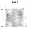
- FIG. 2 is a view for explaining the direction and order of display of image data on a display unit of a mobile communication terminal according to the prior art.
- the display unit of the mobile communication terminal drives 176 pixels in a transverse direction, beginning with the first column address 001 at the left upper end to the last column address 176 at the right upper end.
- the display unit then, with row address 002, sequentially drives the 176 pixels from the first column address to the last column address. This operation of display then continues until row address 240 is reached.
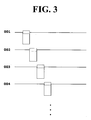
- FIG. 3 is a view showing a timing state for a scan voltage outputted to row electrodes of a display panel according to the related art.
- the row driver of the display panel according to the related art is driven line by line, and thus a scan voltage, beginning with row address 001 up to row address 240, is sequentially outputted to the row electrodes of the display panel based on a horizontal synchronization signal.
- the apparatus for controlling the display unit of the mobile communication terminal has a problem in that, because the display panel is driven line by line beginning from the uppermost line, the display quality in the lower portion of the display screen is degraded relative to the upper portion of the display screen when the display screen receives an insufficient number of bits, which often occurs due to a transmission bit control.
- a feature of a present embodiment is to provide an apparatus and method for driving a display unit of a mobile communication terminal, which improves image quality and reduces manufacturing costs by storing image data in a memory (e.g., a graphic random access memory (GRAM)) by line units of a frame, each line unit including a predetermined number of row lines, and to display the stored image data beginning with a row line at or near the center of the display unit.
- a memory e.g., a graphic random access memory (GRAM)
- an apparatus for driving a display unit of a mobile communication terminal includes a memory that stores image data by line units of a frame, each line unit including a predetermined number of row lines; at least one column driver that receives the stored image data and a vertical synchronization signal and outputs a signal voltage to column addresses based on the received image data and the received vertical synchronization signal; at least one row driver that receives a horizontal synchronization signal corresponding to the vertical synchronization signal and outputs a scan voltage to row addresses based on the received horizontal synchronization signal; and a display panel that displays the image data thereon based on the output signal voltage and the output scan voltage.
- a method for driving a display unit of a mobile communication terminal includes storing image data in a memory by line units of a frame, each line unit including a predetermined number of row lines; receiving the stored image data and a vertical synchronization signal and outputting a signal voltage to column addresses based on the received image data and the received vertical synchronization signal; receiving a horizontal synchronization signal corresponding to the vertical synchronization signal and outputting a scan voltage to row addresses based on the received horizontal synchronization signal; and displaying the image data on a display panel based on the outputted signal voltage and the outputted scan voltage.
- an apparatus for driving a display unit of a mobile communication terminal includes a memory that stores image data by line units of a frame, each line unit including a predetermined number of row lines; at least one column driver that receives the stored image data from the memory, receives a vertical synchronization signal, and outputs signal voltages to column addresses based on the received image data and the received vertical synchronization signal; at least one row driver that receives a horizontal synchronization signal corresponding to the vertical synchronization signal, and outputs scan voltages to row addresses based on the received horizontal synchronization signal; and a processor that cooperates with the memory, the column driver, and the row driver, to display of the image data based on the output signal voltages from the column driver and the scan voltages from the row driver.
- an apparatus and method for driving a display unit of a mobile communication terminal which is configured to improve display image quality and reduce manufacturing costs by storing image data in a memory (e.g., a graphic random access memory (GRAM)) by line units of a frame, each line unit including a predetermined number of row lines, and displaying the stored image data starting from a line at or near the center of the display unit.
- a memory e.g., a graphic random access memory (GRAM)
- GRAM graphic random access memory
- the apparatus and method for driving a display unit of a mobile communication terminal according to the present invention are applicable to various types of display panels with column electrodes and row electrodes that cross each other to form a matrix pattern of pixel cells.
- LCD liquid crystal display
- a typical LCD system may be comprised of an LCD panel having a matrix of pixel cells with RGB filters to enable color reproduction; a backlight driver with a light sensor to provide necessary light to the LCD panel; one or more row drivers to operate the rows of pixel cells; a timing controller with a clock driver to control the necessary timing of the row drivers; one or more column drivers to operate the columns of pixel cells upon receiving image (video) input data; a gamma generator to control the column drivers based upon the non-linear relationship (i.e., a S-shaped gamma curve) between the light emitted from a pixel and the voltage applied to it; and a power supply with a reference voltage generator to supply necessary supply voltages to all these components.
- a backlight driver with a light sensor to provide necessary light to the LCD panel
- one or more row drivers to operate the rows of pixel cells
- a timing controller with a clock driver to control the necessary timing of the row drivers
- one or more column drivers to operate the columns of pixel cells upon receiving image (
- the operation of the LCD system depends upon the row and column drivers, gamma correction, and multiple supply voltages.
- the row drivers are power drivers used to select which row will have its data written at a given time.
- the column drivers convert the digital video data input to the display into an analog voltage to be stored across each pixel cell, whereby the brightness of each pixel is determined by an analog voltage level stored across that pixel.
- the timing controller controls the timing of a scanning mechanism used to handle the writing of data into the LCD panel.
- the related art timing controller resets the row and column drivers to start writing data in at the top of the display and scan one row at a time to the bottom of the display.
- the central region of a display screen may suffer from image quality degradation (compared to other regions of the display screen) due to various factors, including an insufficient number of bits being received due to transmission bit rate controlling.
- the central region of the display may be where relatively important image data are to be displayed (i.e., images that usually have objects of interest are centered on the screen), and thus image quality may be more important at such central regions of the display.
- the present invention enhances and improves the scanning mechanism and the timing controller, based upon how the image (video) data are stored. Namely, instead of storing the image data by a frame as in the related art, the present invention stores image data by line units, each line unit including at least one scan line or row line, whereby a pre-set number of lines within one line unit are stored at a time, instead of storing image data for an entire frame.
- the scanning mechanism and the timing controller operate to control the row and column drivers to start writing data on at least two divided portions of the display screen.
- the present invention starts writing data at a central portion of the display screen.
- the display screen may be divided into at least two portions (sections). These will be referred to as an upper portion and a lower portion merely for the sake of orientation and explanation (as can be understood from Fig. 6 described in more detail later).
- the data writing may begin at the bottom-most row of the upper portion, and may begin at the top-most row of the lower portion. Both of the portions correspond to a relatively central region of the display screen.
- the scanning is proceeded within the upper portion one (or more) row(s) at a time towards the upper end of the overall display screen, and within the lower portion one (or more) row(s) at a time towards the lower end of the overall display screen.
- the scanning may be performed in the upper and lower portions in a relatively simultaneously manner.
- the scanning may be performed in an alternating manner, for each unit of scan row lines of the upper portion and of the lower portion, respectively.
- the overall display screen could be divided into more than two portions, depending upon various factors, such as the size of the display screen, processing capabilities, etc.
- the present invention not only results in improved quality in displayed image portions at a central region of the display screen, but also, the required amount of necessary memory space and power consumption may be reduced.
- Such minimal memory requirements and efficient use of power are important for multimedia communications devices, such as mobile phones, PDAs, and other wireless devices having mobility characteristics and video and image reproduction capabilities.
- Digital multimedia broadcasting (DMB) technologies e.g., satellite DMB, terrestrial DMB, etc.
- downloading streaming videos from Internet servers performing multimedia communications via wireless interfaces (Wi-Fi, Wi-MAX, etc.) and the like, are some non-limiting examples of practical applications that would benefit from the teachings and suggestions of the present invention.
- FIG. 4 is a view showing an apparatus for driving a display unit of a mobile communication terminal according to the present invention.
- the apparatus for driving a display unit of a mobile communication terminal includes: an input device 110 for receiving image data to be displayed; a memory 200 for storing input image data; a controller 100 for receiving the stored image data and a synchronization signal and outputting the received image data and the synchronization signal; a memory (e.g., a graphic random access memory GRAM)) 300 for storing the output image data in units of lines of a predetermined number within a frame; a column driver 400 for receiving the stored image data and the synchronization signal and outputting a signal voltage to column addresses based on the received image data and synchronization signal; a row driver 500 for outputting a scan voltage to row addresses of the output signal voltage based on the received synchronization signal; and a display panel 600 for displaying the received image data thereon based on the scan voltage output from the row driver and the signal voltage output from the column driver.
- the synchronization signal includes a vertical synchronization signal input into the column driver 400 and a horizontal
- FIG. 5 is a flow chart showing an exemplary method for driving a display unit of a mobile communication terminal according to the present invention.
- the method for driving a display unit of a mobile communication terminal includes: storing image data in a memory (e.g., GRAM) by line units of a frame, each line unit including a predetermined number of row lines (S500); applying the stored image data and a vertical synchronization signal to a column driver (S510); providing a horizontal synchronization signal corresponding to the provided vertical synchronization signal to at least one row driver (S520); and outputting the image data to a display panel based on the provided vertical synchronization signal and the provided horizontal synchronization signal (S530).
- a memory e.g., GRAM
- the row driver includes a first row driver that drives an upper portion of the display panel, and a second row driver that drives a lower portion of the display panel.
- the first row driver starts to process image data by beginning with the bottom-most row line of the upper portion, and continues to process up to the top-most row line of the upper portion
- the second row driver starts to process image data by beginning with the top-most row line of the lower portion, and continues to process up to the bottom-most row line of the upper portion.
- the controller 100 is configured to output various operation information for controlling and monitoring each function of the mobile communication terminal, to output messages, such as SMS (Short Message Service) messages or an MMS (multimedia message service) messages and graphical messages to the GRAM 300, and to output a vertical synchronization signal and a horizontal synchronization signal.
- messages such as SMS (Short Message Service) messages or an MMS (multimedia message service) messages and graphical messages to the GRAM 300, and to output a vertical synchronization signal and a horizontal synchronization signal.
- the GRAM 300 receives and stores the image data provided by the controller by line units of a frame, each line unit including a predetermined number of row lines (S500), and outputs the stored image data to the column driver 400.
- the capacity of the GRAM 300 storing image data will be described with an example under an assumption that the display panel 600 has a resolution of 176 x 240 pixels and one pixel is 18 bits long. However, it can be clearly understood that the present invention is applicable to other displays having different resolutions and pixel lengths.
- the GRAM 300 requires a capacity of at least 176 x 240 x 18 bits (i.e., 760,320 bits) in order to store the image data by a frame as in the related art
- the GRAM 300 of the present embodiment only requires a capacity of 176 x 18 bits (i.e., 3,168 bits) to store image data by a line unit including one row line and a capacity of 76 x 2 x 18 bits (i.e., 6,336 bits) to store image data by a line unit including two row lines, and thus can reduce the capacity of the GRAM 300 for temporarily storing image data therein.
- the column driver 400 receives the stored image data and a vertical synchronization signal (S510). The column driver 400 then outputs the image data by a frame of column lines to the display panel 600 in a vertical direction according to the applied vertical synchronization signal applied in the order of column addresses.
- the column driver 400 drives column electrodes 610 of the display panel 600, and serves to actually apply image data, i.e., a signal voltage to each pixel of the display panel 600 through the column electrodes 610.
- the row driver 500 receives a horizontal synchronization signal corresponding to the applied vertical synchronization signal (S520). The row driver 500 then disperses the image data outputted by the frame of column lines in the vertical direction of the display panel 600 by the column driver 400 in a horizontal direction based on the applied horizontal synchronization signal in a predetermined order of row addresses. The row driver 500 generates scan signals for sequentially selecting the row electrodes 620 and drives the row electrodes 620.
- the row driver 500 divides the total number of row address into two sections, and employs a first row driver 510 that first processes the image data associated with a substantially center line of the display panel and then keeps processing the image in an upward direction, and employs a second row driver 520 that first processes the image data associated with substantially a center line of the display panel and then keeps processing the image data towards a downward direction.
- a first row driver 510 that first processes the image data associated with a substantially center line of the display panel and then keeps processing the image in an upward direction
- a second row driver 520 that first processes the image data associated with substantially a center line of the display panel and then keeps processing the image data towards a downward direction.
- FIG. 6 is a view for explaining the direction and order of display of image data on a display unit of a mobile communication terminal according to the present invention.
- the display unit having the row lines is divided into two large regions (i.e., upper and lower portions).
- the lines of the upper portion are driven by the first row driver and the lines of the lower portion are driven by the second row driver in up and down directions or in down and up directions in an alternating manner.
- the bottom-most row address 120 of the upper portion begins to be processed by the first row driver, and the top-most row address 121 of the lower portion is then processed by the second row driver.
- the row address 119 of the upper portion and the row address 122 of the lower portion are sequentially processed, respectively. This alternate process is then continued until the row address 001 of the upper portion and the row address 240 of the lower portion are processed.
- the GRAM requires a capacity of at least 176 x 18 bits (i.e., 3,168 bits) in order to store image data provided in a line unit of row lines in one frame.
- the lines at the upper portion driven by the first row driver and the lines at the lower portion driven by the second row driver may be processed in up and down directions in an alternating manner by a line unit containing two row lines.
- the two bottom-most row addresses 120 and 119 of the upper portion begin to be processed by the first row driver, and the two top-most row addresses 121 and 122 of the lower portion are then processed by the second row driver.
- the two row addresses next to the two bottom-most row addresses 120 and 119 of the upper portion and the two addresses next to the row addresses 122 and 121 of the lower portion are sequentially processed, respectively. This alternate process is then continued until the row address 001 of the upper portion and the row address 240 of the lower portion are processed.
- the GRAM requires a capacity of at least 176 x 18 x 2 bits (i.e., 6,336 bits) in order to store image data provided in a line unit including two row lines of one frame.
- FIGs. 7A to 7D are views showing a timing state for a scan voltage outputted to row electrodes of a display panel according to the present invention.
- FIG. 7A shows the scan voltage is outputted by beginning with the row address 120 in the upper portion line by line in an alternating manner between the upward direction in the upper portion and the downward direction in the lower portion.
- FIG. 7B shows the scan voltage is outputted by beginning with the row address 121 in the lower portion line by line in an alternating manner between the downward direction in the lower portion and the upward direction in the upper portion.
- FIG. 7C shows the scan voltage is outputted by beginning with the row addresses 120 and 119 in the upper portion two-line by two-line in an alternating manner between the upward direction in the upper portion and the downward direction in the lower portion.
- FIG. 7D shows the scan voltage is outputted by beginning with the row addresses 121 and 122 in the lower portion two-line-by two-line in an alternating manner between the downward direction in the lower portion and the upward direction in the upper portion.
- the row addresses of the display unit 600 of the mobile communication terminal are divided into two portions, the row addresses at the upper portion are driven by the first row driver 510 in upward direction and the row addresses at the lower portion are driven by the second row driver 520 in downward direction and the upper and lower portions are driven in an alternating manner by at least one line unit including at least at least one row address.
- the display panel 600 is configured by units of pixels, in which column electrodes 610 and row electrodes 620 cross each other, and can display the image data by the column driver 400 applying a signal voltage to the column electrodes 610 and the first and second row drivers 510 and 520 applying a scan voltage to the row electrodes 620 (S530).
- the column driver 400 of the display unit may divided into a right portion and a left portion configured to be driven by a first column driver and a second column driver, respectively.
- the apparatus and method for driving a display unit of a mobile communication terminal improves the image quality efficiently by relatively minimizing errors occurring at or near the center region of the screen (where the user's view is typically focused on) by storing image data in a GRAM line units of a frame, each line unit including a predetermined number of row lines and displaying the stored image data, starting from the line at or near the center of the display unit.
- the apparatus and method for driving a display unit of a mobile communication terminal can reduce manufacturing costs since the capacity of a GRAM storing image data can be reduced by storing image data in a GRAM by line units of a frame, each line unit including a predetermined number row lines and displaying the stored image data, starting from the line at or near the center of the display unit.
- inventions of the disclosure may be referred to herein, individually and/or collectively, by the term "invention" merely for convenience and without intending to voluntarily limit the scope of this application to any particular invention or inventive concept.
- inventions may be referred to herein, individually and/or collectively, by the term "invention" merely for convenience and without intending to voluntarily limit the scope of this application to any particular invention or inventive concept.
- specific embodiments have been illustrated and described herein, it should be appreciated that any subsequent arrangement designed to achieve the same or similar purpose may be substituted for the specific embodiments shown.
- This disclosure is intended to cover any and all subsequent adaptations or variations of various embodiments. Combinations of the above embodiments, and other embodiments not specifically described herein, will be apparent to those of skill in the art upon reviewing the description.
Landscapes
- Engineering & Computer Science (AREA)
- Physics & Mathematics (AREA)
- Computer Hardware Design (AREA)
- General Physics & Mathematics (AREA)
- Theoretical Computer Science (AREA)
- Signal Processing (AREA)
- Computer Networks & Wireless Communication (AREA)
- Chemical & Material Sciences (AREA)
- Crystallography & Structural Chemistry (AREA)
- Control Of Indicators Other Than Cathode Ray Tubes (AREA)
- Control Of El Displays (AREA)
- Control Of Gas Discharge Display Tubes (AREA)
- Liquid Crystal (AREA)
- Liquid Crystal Display Device Control (AREA)
Applications Claiming Priority (1)
| Application Number | Priority Date | Filing Date | Title |
|---|---|---|---|
| KR1020040103144A KR100621020B1 (ko) | 2004-12-08 | 2004-12-08 | 휴대단말기의 표시부 제어장치 및 방법 |
Publications (1)
| Publication Number | Publication Date |
|---|---|
| EP1669967A2 true EP1669967A2 (de) | 2006-06-14 |
Family
ID=36118265
Family Applications (1)
| Application Number | Title | Priority Date | Filing Date |
|---|---|---|---|
| EP05026763A Withdrawn EP1669967A2 (de) | 2004-12-08 | 2005-12-07 | Vorrichtung und Verfahren zur Ansteuerung einer Anzeigeeinheit eines mobilen Kommunikationsendgeräts |
Country Status (5)
| Country | Link |
|---|---|
| US (1) | US20060119706A1 (de) |
| EP (1) | EP1669967A2 (de) |
| JP (1) | JP2006163385A (de) |
| KR (1) | KR100621020B1 (de) |
| CN (1) | CN1787061A (de) |
Cited By (1)
| Publication number | Priority date | Publication date | Assignee | Title |
|---|---|---|---|---|
| EP2793215A1 (de) * | 2013-04-17 | 2014-10-22 | Samsung Display Co., Ltd. | Scan-Treiber und organische lichtemittierende Anzeigevorrichtung damit |
Families Citing this family (11)
| Publication number | Priority date | Publication date | Assignee | Title |
|---|---|---|---|---|
| KR100739183B1 (ko) * | 2005-12-30 | 2007-07-13 | 엘지전자 주식회사 | 제 2 통신 모듈의 활성화에 따라, 제 1 통신 모듈의 전력을절감할 수 있도록 한 이동통신 단말기 및 방법 |
| CN101809646B (zh) * | 2007-11-07 | 2012-09-26 | 夏普株式会社 | 显示装置、液晶显示装置、电视接收机 |
| TWI421820B (zh) * | 2009-10-16 | 2014-01-01 | Ind Tech Res Inst | 顯示裝置、電子系統以及控制方法 |
| CN102479491B (zh) * | 2010-11-23 | 2013-09-11 | 汉王科技股份有限公司 | 一种双源同屏显示的液晶显示屏及液晶显示装置 |
| CN102820020B (zh) * | 2011-06-08 | 2015-05-27 | 天津三星电子有限公司 | 一种可实现双桌面操作功能的显示器 |
| KR102263319B1 (ko) * | 2015-01-30 | 2021-06-09 | 삼성전자주식회사 | 디스플레이 잡음을 개선하는 디스플레이 컨트롤러, 및 상기 디스플레이 컨트롤러를 포함하는 시스템 |
| JP6543522B2 (ja) | 2015-07-06 | 2019-07-10 | 株式会社ジャパンディスプレイ | 表示装置 |
| JP2019020447A (ja) * | 2017-07-11 | 2019-02-07 | 株式会社ジャパンディスプレイ | 表示装置の駆動方法及び表示装置 |
| CN108717838B (zh) * | 2018-04-17 | 2021-05-25 | 昀光微电子(上海)有限公司 | 一种硅基微型显示器及其驱动电路 |
| KR102777822B1 (ko) * | 2018-10-08 | 2025-03-06 | 엘지디스플레이 주식회사 | 표시 장치 |
| CN112634820A (zh) * | 2020-12-23 | 2021-04-09 | 深圳市奥视微科技有限公司 | 显示装置及电子设备 |
Family Cites Families (4)
| Publication number | Priority date | Publication date | Assignee | Title |
|---|---|---|---|---|
| JP3710728B2 (ja) * | 2001-06-29 | 2005-10-26 | シャープ株式会社 | 液晶駆動装置 |
| JP3879484B2 (ja) * | 2001-10-30 | 2007-02-14 | 株式会社日立製作所 | 液晶表示装置 |
| KR20030080146A (ko) * | 2002-04-04 | 2003-10-11 | 엘지전자 주식회사 | 패시브 매트릭스 구조를 갖는 유기 el 디스플레이장치의 스캔 방법 |
| JP4754772B2 (ja) * | 2003-05-16 | 2011-08-24 | 株式会社半導体エネルギー研究所 | 発光装置及び該発光装置を用いた電子機器 |
-
2004
- 2004-12-08 KR KR1020040103144A patent/KR100621020B1/ko not_active Expired - Fee Related
-
2005
- 2005-11-21 JP JP2005336245A patent/JP2006163385A/ja active Pending
- 2005-12-07 EP EP05026763A patent/EP1669967A2/de not_active Withdrawn
- 2005-12-07 US US11/295,564 patent/US20060119706A1/en not_active Abandoned
- 2005-12-08 CN CNA2005101297266A patent/CN1787061A/zh active Pending
Cited By (1)
| Publication number | Priority date | Publication date | Assignee | Title |
|---|---|---|---|---|
| EP2793215A1 (de) * | 2013-04-17 | 2014-10-22 | Samsung Display Co., Ltd. | Scan-Treiber und organische lichtemittierende Anzeigevorrichtung damit |
Also Published As
| Publication number | Publication date |
|---|---|
| US20060119706A1 (en) | 2006-06-08 |
| KR20060064332A (ko) | 2006-06-13 |
| JP2006163385A (ja) | 2006-06-22 |
| CN1787061A (zh) | 2006-06-14 |
| KR100621020B1 (ko) | 2006-09-19 |
Similar Documents
| Publication | Publication Date | Title |
|---|---|---|
| KR100499845B1 (ko) | 액티브 매트릭스형 표시 장치 및 그 제어 장치 | |
| US7071930B2 (en) | Active matrix display device, video signal processing device, method of driving the active matrix display device, method of processing signal, computer program executed for driving the active matrix display device, and storage medium storing the computer program | |
| US8421791B2 (en) | Liquid crystal display device | |
| KR100610954B1 (ko) | 표시 장치 및 표시 장치의 구동 방법 | |
| JP4109616B2 (ja) | 表示用の黒画像挿入方法および装置 | |
| US8013829B2 (en) | Liquid crystal display having black insertion controller selecting black insertion control signals according to data stored therein and driving method thereof | |
| EP1669967A2 (de) | Vorrichtung und Verfahren zur Ansteuerung einer Anzeigeeinheit eines mobilen Kommunikationsendgeräts | |
| JP2003255915A (ja) | 表示装置及びその駆動方法 | |
| US20140028736A1 (en) | Liquid crystal display and 3d imaging apparatus and operating methods thereof | |
| JP2007333997A (ja) | 表示制御装置、表示装置、端末装置、表示制御方法及びコンピュータプログラム | |
| JP4566176B2 (ja) | 表示駆動回路 | |
| US20110205213A1 (en) | Liquid crystal display device | |
| US20050078070A1 (en) | System and method for driving a display panel of mobile terminal | |
| US20100328559A1 (en) | Display device and drive control device thereof, scan signal line driving method, and drive circuit | |
| US20070080915A1 (en) | Display driver, electro-optical device, electronic instrument, and drive method | |
| JP4910466B2 (ja) | 表示駆動装置 | |
| JP2008020573A (ja) | 電気光学装置および電子機器 | |
| US20120113319A1 (en) | Display device and display method | |
| CN107331340B (zh) | 一种显示面板的驱动控制方法及驱动控制装置 | |
| US20090002353A1 (en) | Display apparatus and drive method thereof | |
| US12462737B2 (en) | Image display apparatus, and video wall including the same | |
| JP5230949B2 (ja) | 携帯電子機器 | |
| US11107393B1 (en) | LED panel controlling method and LED panel controlling system | |
| JP2010008598A (ja) | 映像表示装置 | |
| JP2008278046A (ja) | 携帯電子機器 |
Legal Events
| Date | Code | Title | Description |
|---|---|---|---|
| PUAI | Public reference made under article 153(3) epc to a published international application that has entered the european phase |
Free format text: ORIGINAL CODE: 0009012 |
|
| AK | Designated contracting states |
Kind code of ref document: A2 Designated state(s): AT BE BG CH CY CZ DE DK EE ES FI FR GB GR HU IE IS IT LI LT LU LV MC NL PL PT RO SE SI SK TR |
|
| AX | Request for extension of the european patent |
Extension state: AL BA HR MK YU |
|
| RIN1 | Information on inventor provided before grant (corrected) |
Inventor name: AN, JIN-WOO |
|
| RIN1 | Information on inventor provided before grant (corrected) |
Inventor name: AN, JIN-WOO |
|
| RIN1 | Information on inventor provided before grant (corrected) |
Inventor name: AN, JIN-WOOGASAN PATENT GROUP, LG ELECTRONICS INC |
|
| STAA | Information on the status of an ep patent application or granted ep patent |
Free format text: STATUS: THE APPLICATION HAS BEEN WITHDRAWN |
|
| 18W | Application withdrawn |
Effective date: 20081210 |