EP1662468A2 - OLED Anzeige mit aktiver Matrix und elektronisches Gerät - Google Patents
OLED Anzeige mit aktiver Matrix und elektronisches Gerät Download PDFInfo
- Publication number
- EP1662468A2 EP1662468A2 EP05025577A EP05025577A EP1662468A2 EP 1662468 A2 EP1662468 A2 EP 1662468A2 EP 05025577 A EP05025577 A EP 05025577A EP 05025577 A EP05025577 A EP 05025577A EP 1662468 A2 EP1662468 A2 EP 1662468A2
- Authority
- EP
- European Patent Office
- Prior art keywords
- display device
- video signal
- signal
- gate driver
- pixels
- Prior art date
- Legal status (The legal status is an assumption and is not a legal conclusion. Google has not performed a legal analysis and makes no representation as to the accuracy of the status listed.)
- Granted
Links
- 229920001621 AMOLED Polymers 0.000 title 1
- 238000005070 sampling Methods 0.000 claims abstract description 62
- 239000011159 matrix material Substances 0.000 claims abstract description 24
- 239000000872 buffer Substances 0.000 claims description 60
- 238000012360 testing method Methods 0.000 claims description 33
- 238000000034 method Methods 0.000 abstract description 19
- 230000015654 memory Effects 0.000 description 11
- 238000010586 diagram Methods 0.000 description 5
- 239000004973 liquid crystal related substance Substances 0.000 description 3
- 238000012545 processing Methods 0.000 description 3
- 238000006243 chemical reaction Methods 0.000 description 2
- 230000000694 effects Effects 0.000 description 2
- 230000006870 function Effects 0.000 description 2
- 238000012986 modification Methods 0.000 description 2
- 230000004048 modification Effects 0.000 description 2
- 239000004065 semiconductor Substances 0.000 description 2
- 238000012546 transfer Methods 0.000 description 2
- 239000003990 capacitor Substances 0.000 description 1
- 238000012937 correction Methods 0.000 description 1
- 238000001514 detection method Methods 0.000 description 1
- 238000007599 discharging Methods 0.000 description 1
- 238000005401 electroluminescence Methods 0.000 description 1
- 239000010408 film Substances 0.000 description 1
- 239000010409 thin film Substances 0.000 description 1
Images


Classifications
-
- G—PHYSICS
- G09—EDUCATION; CRYPTOGRAPHY; DISPLAY; ADVERTISING; SEALS
- G09G—ARRANGEMENTS OR CIRCUITS FOR CONTROL OF INDICATING DEVICES USING STATIC MEANS TO PRESENT VARIABLE INFORMATION
- G09G3/00—Control arrangements or circuits, of interest only in connection with visual indicators other than cathode-ray tubes
- G09G3/20—Control arrangements or circuits, of interest only in connection with visual indicators other than cathode-ray tubes for presentation of an assembly of a number of characters, e.g. a page, by composing the assembly by combination of individual elements arranged in a matrix no fixed position being assigned to or needed to be assigned to the individual characters or partial characters
-
- G—PHYSICS
- G09—EDUCATION; CRYPTOGRAPHY; DISPLAY; ADVERTISING; SEALS
- G09G—ARRANGEMENTS OR CIRCUITS FOR CONTROL OF INDICATING DEVICES USING STATIC MEANS TO PRESENT VARIABLE INFORMATION
- G09G3/00—Control arrangements or circuits, of interest only in connection with visual indicators other than cathode-ray tubes
- G09G3/20—Control arrangements or circuits, of interest only in connection with visual indicators other than cathode-ray tubes for presentation of an assembly of a number of characters, e.g. a page, by composing the assembly by combination of individual elements arranged in a matrix no fixed position being assigned to or needed to be assigned to the individual characters or partial characters
- G09G3/22—Control arrangements or circuits, of interest only in connection with visual indicators other than cathode-ray tubes for presentation of an assembly of a number of characters, e.g. a page, by composing the assembly by combination of individual elements arranged in a matrix no fixed position being assigned to or needed to be assigned to the individual characters or partial characters using controlled light sources
- G09G3/30—Control arrangements or circuits, of interest only in connection with visual indicators other than cathode-ray tubes for presentation of an assembly of a number of characters, e.g. a page, by composing the assembly by combination of individual elements arranged in a matrix no fixed position being assigned to or needed to be assigned to the individual characters or partial characters using controlled light sources using electroluminescent panels
- G09G3/32—Control arrangements or circuits, of interest only in connection with visual indicators other than cathode-ray tubes for presentation of an assembly of a number of characters, e.g. a page, by composing the assembly by combination of individual elements arranged in a matrix no fixed position being assigned to or needed to be assigned to the individual characters or partial characters using controlled light sources using electroluminescent panels semiconductive, e.g. using light-emitting diodes [LED]
- G09G3/3208—Control arrangements or circuits, of interest only in connection with visual indicators other than cathode-ray tubes for presentation of an assembly of a number of characters, e.g. a page, by composing the assembly by combination of individual elements arranged in a matrix no fixed position being assigned to or needed to be assigned to the individual characters or partial characters using controlled light sources using electroluminescent panels semiconductive, e.g. using light-emitting diodes [LED] organic, e.g. using organic light-emitting diodes [OLED]
- G09G3/3225—Control arrangements or circuits, of interest only in connection with visual indicators other than cathode-ray tubes for presentation of an assembly of a number of characters, e.g. a page, by composing the assembly by combination of individual elements arranged in a matrix no fixed position being assigned to or needed to be assigned to the individual characters or partial characters using controlled light sources using electroluminescent panels semiconductive, e.g. using light-emitting diodes [LED] organic, e.g. using organic light-emitting diodes [OLED] using an active matrix
-
- G—PHYSICS
- G09—EDUCATION; CRYPTOGRAPHY; DISPLAY; ADVERTISING; SEALS
- G09G—ARRANGEMENTS OR CIRCUITS FOR CONTROL OF INDICATING DEVICES USING STATIC MEANS TO PRESENT VARIABLE INFORMATION
- G09G3/00—Control arrangements or circuits, of interest only in connection with visual indicators other than cathode-ray tubes
- G09G3/20—Control arrangements or circuits, of interest only in connection with visual indicators other than cathode-ray tubes for presentation of an assembly of a number of characters, e.g. a page, by composing the assembly by combination of individual elements arranged in a matrix no fixed position being assigned to or needed to be assigned to the individual characters or partial characters
- G09G3/2092—Details of a display terminals using a flat panel, the details relating to the control arrangement of the display terminal and to the interfaces thereto
-
- G—PHYSICS
- G09—EDUCATION; CRYPTOGRAPHY; DISPLAY; ADVERTISING; SEALS
- G09G—ARRANGEMENTS OR CIRCUITS FOR CONTROL OF INDICATING DEVICES USING STATIC MEANS TO PRESENT VARIABLE INFORMATION
- G09G3/00—Control arrangements or circuits, of interest only in connection with visual indicators other than cathode-ray tubes
- G09G3/20—Control arrangements or circuits, of interest only in connection with visual indicators other than cathode-ray tubes for presentation of an assembly of a number of characters, e.g. a page, by composing the assembly by combination of individual elements arranged in a matrix no fixed position being assigned to or needed to be assigned to the individual characters or partial characters
- G09G3/22—Control arrangements or circuits, of interest only in connection with visual indicators other than cathode-ray tubes for presentation of an assembly of a number of characters, e.g. a page, by composing the assembly by combination of individual elements arranged in a matrix no fixed position being assigned to or needed to be assigned to the individual characters or partial characters using controlled light sources
- G09G3/30—Control arrangements or circuits, of interest only in connection with visual indicators other than cathode-ray tubes for presentation of an assembly of a number of characters, e.g. a page, by composing the assembly by combination of individual elements arranged in a matrix no fixed position being assigned to or needed to be assigned to the individual characters or partial characters using controlled light sources using electroluminescent panels
-
- G—PHYSICS
- G09—EDUCATION; CRYPTOGRAPHY; DISPLAY; ADVERTISING; SEALS
- G09G—ARRANGEMENTS OR CIRCUITS FOR CONTROL OF INDICATING DEVICES USING STATIC MEANS TO PRESENT VARIABLE INFORMATION
- G09G3/00—Control arrangements or circuits, of interest only in connection with visual indicators other than cathode-ray tubes
- G09G3/20—Control arrangements or circuits, of interest only in connection with visual indicators other than cathode-ray tubes for presentation of an assembly of a number of characters, e.g. a page, by composing the assembly by combination of individual elements arranged in a matrix no fixed position being assigned to or needed to be assigned to the individual characters or partial characters
- G09G3/22—Control arrangements or circuits, of interest only in connection with visual indicators other than cathode-ray tubes for presentation of an assembly of a number of characters, e.g. a page, by composing the assembly by combination of individual elements arranged in a matrix no fixed position being assigned to or needed to be assigned to the individual characters or partial characters using controlled light sources
- G09G3/30—Control arrangements or circuits, of interest only in connection with visual indicators other than cathode-ray tubes for presentation of an assembly of a number of characters, e.g. a page, by composing the assembly by combination of individual elements arranged in a matrix no fixed position being assigned to or needed to be assigned to the individual characters or partial characters using controlled light sources using electroluminescent panels
- G09G3/32—Control arrangements or circuits, of interest only in connection with visual indicators other than cathode-ray tubes for presentation of an assembly of a number of characters, e.g. a page, by composing the assembly by combination of individual elements arranged in a matrix no fixed position being assigned to or needed to be assigned to the individual characters or partial characters using controlled light sources using electroluminescent panels semiconductive, e.g. using light-emitting diodes [LED]
- G09G3/3208—Control arrangements or circuits, of interest only in connection with visual indicators other than cathode-ray tubes for presentation of an assembly of a number of characters, e.g. a page, by composing the assembly by combination of individual elements arranged in a matrix no fixed position being assigned to or needed to be assigned to the individual characters or partial characters using controlled light sources using electroluminescent panels semiconductive, e.g. using light-emitting diodes [LED] organic, e.g. using organic light-emitting diodes [OLED]
- G09G3/3275—Details of drivers for data electrodes
-
- G—PHYSICS
- G09—EDUCATION; CRYPTOGRAPHY; DISPLAY; ADVERTISING; SEALS
- G09G—ARRANGEMENTS OR CIRCUITS FOR CONTROL OF INDICATING DEVICES USING STATIC MEANS TO PRESENT VARIABLE INFORMATION
- G09G3/00—Control arrangements or circuits, of interest only in connection with visual indicators other than cathode-ray tubes
- G09G3/20—Control arrangements or circuits, of interest only in connection with visual indicators other than cathode-ray tubes for presentation of an assembly of a number of characters, e.g. a page, by composing the assembly by combination of individual elements arranged in a matrix no fixed position being assigned to or needed to be assigned to the individual characters or partial characters
- G09G3/34—Control arrangements or circuits, of interest only in connection with visual indicators other than cathode-ray tubes for presentation of an assembly of a number of characters, e.g. a page, by composing the assembly by combination of individual elements arranged in a matrix no fixed position being assigned to or needed to be assigned to the individual characters or partial characters by control of light from an independent source
- G09G3/36—Control arrangements or circuits, of interest only in connection with visual indicators other than cathode-ray tubes for presentation of an assembly of a number of characters, e.g. a page, by composing the assembly by combination of individual elements arranged in a matrix no fixed position being assigned to or needed to be assigned to the individual characters or partial characters by control of light from an independent source using liquid crystals
-
- G—PHYSICS
- G09—EDUCATION; CRYPTOGRAPHY; DISPLAY; ADVERTISING; SEALS
- G09G—ARRANGEMENTS OR CIRCUITS FOR CONTROL OF INDICATING DEVICES USING STATIC MEANS TO PRESENT VARIABLE INFORMATION
- G09G2300/00—Aspects of the constitution of display devices
- G09G2300/08—Active matrix structure, i.e. with use of active elements, inclusive of non-linear two terminal elements, in the pixels together with light emitting or modulating elements
-
- G—PHYSICS
- G09—EDUCATION; CRYPTOGRAPHY; DISPLAY; ADVERTISING; SEALS
- G09G—ARRANGEMENTS OR CIRCUITS FOR CONTROL OF INDICATING DEVICES USING STATIC MEANS TO PRESENT VARIABLE INFORMATION
- G09G2300/00—Aspects of the constitution of display devices
- G09G2300/08—Active matrix structure, i.e. with use of active elements, inclusive of non-linear two terminal elements, in the pixels together with light emitting or modulating elements
- G09G2300/0809—Several active elements per pixel in active matrix panels
-
- G—PHYSICS
- G09—EDUCATION; CRYPTOGRAPHY; DISPLAY; ADVERTISING; SEALS
- G09G—ARRANGEMENTS OR CIRCUITS FOR CONTROL OF INDICATING DEVICES USING STATIC MEANS TO PRESENT VARIABLE INFORMATION
- G09G2310/00—Command of the display device
- G09G2310/06—Details of flat display driving waveforms
- G09G2310/061—Details of flat display driving waveforms for resetting or blanking
- G09G2310/063—Waveforms for resetting the whole screen at once
-
- G—PHYSICS
- G09—EDUCATION; CRYPTOGRAPHY; DISPLAY; ADVERTISING; SEALS
- G09G—ARRANGEMENTS OR CIRCUITS FOR CONTROL OF INDICATING DEVICES USING STATIC MEANS TO PRESENT VARIABLE INFORMATION
- G09G2320/00—Control of display operating conditions
- G09G2320/04—Maintaining the quality of display appearance
- G09G2320/041—Temperature compensation
-
- G—PHYSICS
- G09—EDUCATION; CRYPTOGRAPHY; DISPLAY; ADVERTISING; SEALS
- G09G—ARRANGEMENTS OR CIRCUITS FOR CONTROL OF INDICATING DEVICES USING STATIC MEANS TO PRESENT VARIABLE INFORMATION
- G09G2330/00—Aspects of power supply; Aspects of display protection and defect management
- G09G2330/02—Details of power systems and of start or stop of display operation
- G09G2330/021—Power management, e.g. power saving
-
- G—PHYSICS
- G09—EDUCATION; CRYPTOGRAPHY; DISPLAY; ADVERTISING; SEALS
- G09G—ARRANGEMENTS OR CIRCUITS FOR CONTROL OF INDICATING DEVICES USING STATIC MEANS TO PRESENT VARIABLE INFORMATION
- G09G2330/00—Aspects of power supply; Aspects of display protection and defect management
- G09G2330/02—Details of power systems and of start or stop of display operation
- G09G2330/021—Power management, e.g. power saving
- G09G2330/022—Power management, e.g. power saving in absence of operation, e.g. no data being entered during a predetermined time
-
- G—PHYSICS
- G09—EDUCATION; CRYPTOGRAPHY; DISPLAY; ADVERTISING; SEALS
- G09G—ARRANGEMENTS OR CIRCUITS FOR CONTROL OF INDICATING DEVICES USING STATIC MEANS TO PRESENT VARIABLE INFORMATION
- G09G2360/00—Aspects of the architecture of display systems
- G09G2360/18—Use of a frame buffer in a display terminal, inclusive of the display panel
-
- G—PHYSICS
- G09—EDUCATION; CRYPTOGRAPHY; DISPLAY; ADVERTISING; SEALS
- G09G—ARRANGEMENTS OR CIRCUITS FOR CONTROL OF INDICATING DEVICES USING STATIC MEANS TO PRESENT VARIABLE INFORMATION
- G09G3/00—Control arrangements or circuits, of interest only in connection with visual indicators other than cathode-ray tubes
- G09G3/20—Control arrangements or circuits, of interest only in connection with visual indicators other than cathode-ray tubes for presentation of an assembly of a number of characters, e.g. a page, by composing the assembly by combination of individual elements arranged in a matrix no fixed position being assigned to or needed to be assigned to the individual characters or partial characters
- G09G3/2007—Display of intermediate tones
- G09G3/2018—Display of intermediate tones by time modulation using two or more time intervals
- G09G3/2022—Display of intermediate tones by time modulation using two or more time intervals using sub-frames
-
- G—PHYSICS
- G09—EDUCATION; CRYPTOGRAPHY; DISPLAY; ADVERTISING; SEALS
- G09G—ARRANGEMENTS OR CIRCUITS FOR CONTROL OF INDICATING DEVICES USING STATIC MEANS TO PRESENT VARIABLE INFORMATION
- G09G3/00—Control arrangements or circuits, of interest only in connection with visual indicators other than cathode-ray tubes
- G09G3/20—Control arrangements or circuits, of interest only in connection with visual indicators other than cathode-ray tubes for presentation of an assembly of a number of characters, e.g. a page, by composing the assembly by combination of individual elements arranged in a matrix no fixed position being assigned to or needed to be assigned to the individual characters or partial characters
- G09G3/22—Control arrangements or circuits, of interest only in connection with visual indicators other than cathode-ray tubes for presentation of an assembly of a number of characters, e.g. a page, by composing the assembly by combination of individual elements arranged in a matrix no fixed position being assigned to or needed to be assigned to the individual characters or partial characters using controlled light sources
- G09G3/30—Control arrangements or circuits, of interest only in connection with visual indicators other than cathode-ray tubes for presentation of an assembly of a number of characters, e.g. a page, by composing the assembly by combination of individual elements arranged in a matrix no fixed position being assigned to or needed to be assigned to the individual characters or partial characters using controlled light sources using electroluminescent panels
- G09G3/32—Control arrangements or circuits, of interest only in connection with visual indicators other than cathode-ray tubes for presentation of an assembly of a number of characters, e.g. a page, by composing the assembly by combination of individual elements arranged in a matrix no fixed position being assigned to or needed to be assigned to the individual characters or partial characters using controlled light sources using electroluminescent panels semiconductive, e.g. using light-emitting diodes [LED]
- G09G3/3208—Control arrangements or circuits, of interest only in connection with visual indicators other than cathode-ray tubes for presentation of an assembly of a number of characters, e.g. a page, by composing the assembly by combination of individual elements arranged in a matrix no fixed position being assigned to or needed to be assigned to the individual characters or partial characters using controlled light sources using electroluminescent panels semiconductive, e.g. using light-emitting diodes [LED] organic, e.g. using organic light-emitting diodes [OLED]
- G09G3/3266—Details of drivers for scan electrodes
Definitions
- the present invention relates to a display device which has a plurality of pixels arranged in matrix, and to an electronic apparatus using the display device. More specifically, the invention relates to a display device which controls each pixel by inputting a video signal to a selected pixel and displays an image, and to an electronic apparatus using the display device.
- an EL display device which has a pixel including an organic electroluminescence element (hereinafter referred to as an organic EL) has started to be put into practical use as a next generation display device substituted for the liquid crystal display device.
- a dot matrix display device has a passive matrix type and an active matrix type.
- an analog grayscale method and a digital grayscale method as a method for achieving grayscale in an active matrix display device.
- grayscale is achieved by controlling the luminance of a pixel.
- each pixel is controlled by two values depending on whether light is emitted or not.
- the grayscale is achieved in accordance with the size of a light emitting area or the length of a light emitting time in a certain period.
- the former is called an area grayscale method and the latter is called a time grayscale method.
- one frame period is divided into a plurality of subframe periods to weight the light emitting time in each subframe period. Then, in accordance with a combination of the subframe periods, luminance per one frame period is controlled to achieve grayscale.
- Patent Documents 1 and 2 disclose one of the methods for achieving multi-grayscale in this manner.
- Patent Document 1 Japanese Patent Laid-Open Publication No. 2001-5426
- Patent Document 2 Japanese Patent Laid-Open Publication No. 2001-324958
- one frame period is divided into six subframe periods (SF1 to SF6) and the length of a light emitting period in each subframe period is set to 2 5 : 2 4 : 2 3 : 2 2 : 2 : 1 to display each grayscale level by selecting a subframe period during which light is emitted (see FIG 5A). Specifically, if no light is emitted in all the periods, a first grayscale level (black: luminance 0) is displayed, while if light is emitted in all the periods, a 64th grayscale level (white: luminance 63) is displayed.
- a 30th grayscale level is displayed.
- the 64 grayscale levels from luminance 0 to luminance 63, 2 4 + 2 3 + 2 2 + 1 29, that is, the 30th grayscale level (luminance 29) is displayed.
- one row selection period is divided into a plurality of sub-horizontal periods (see FIG. 5B, in FIG 5B, one row selection period is divided into two sub-horizontal periods), writing of a video signal is performed in a certain sub-horizontal period while erasing is performed in another sub-horizontal period. Each of the writing and the erasing is performed in a required row at a required timing to control a light emitting period in each bit.
- an active matrix type pixel may be driven by two values of white display and black display. Therefore, it is highly advantageous that characteristic variations of thin film transistors (hereinafter referred to as TFTs) which form a pixel hardly affect display quality.
- TFTs thin film transistors
- writing operation, erasing operation and the like for controlling light emitting time are required, and the number of times of writing a video signal in one frame period increases. Accordingly, the operating frequency of a periphery driver circuit and power consumption increase.
- the number of the writing operations and the erasing operations usually increases and power consumption increases as well.
- the aforementioned organic EL display device and the like are expected to be mounted on a mobile phone, a PDA (personal digital assistant), a portable audio player and the like by taking advantage of light weight and thin shape.
- a mobile phone a PDA (personal digital assistant)
- PDA personal digital assistant
- portable audio player a portable audio player and the like by taking advantage of light weight and thin shape.
- high power consumption may affect a continuous using time. Therefore, high power consumption is a critical problem.
- the invention provides a display device which can reduce power consumption in the case of being driven by using the digital time grayscale method, and an electronic apparatus using the display device. Further, the invention provides a display device which can reduce power consumption in a display state which seems to be frequently used in an actual portable terminal, such as a text display, and an electronic apparatus using the display device.
- a driving method is used, where one horizontal period is divided into a plurality of (for example, two) sub-horizontal periods, writing of a video signal is performed in one sub-horizontal period, and erasing is preformed in the other sub-horizontal period.
- a video signal and an erasing signal are alternately outputted to a source signal line.
- an erasing signal is certainly outputted to all the source signal lines.
- the erasing signal inputted immediately before is used in the pixels arranged in the row to display black instead of the video signal for displaying black.
- a display device of the invention has a display portion having a plurality of pixels arranged in matrix, a shift register for outputting a sampling pulse, and a latch circuit for sampling video signals (all the video signals) in accordance with the sampling pulse, a line buffer circuit for holding video signals (one-row video signals) outputted to each of the plurality of pixels arranged in the same row, and a test circuit for testing the video signals (one-row video signals) held in the line buffer circuit.
- the test circuit outputs a control signal so that the shift register stops the output of the sampling pulse to the plurality of pixels arranged in the row.
- a display device of the invention has a display portion having a plurality of pixels arranged in matrix, a shift register for outputting a sampling pulse, and a latch circuit for sampling video signals (all the video signals) in accordance with the sampling pulse, a line buffer circuit for holding video signals (one-row video signals) outputted to each of the plurality of pixels arranged in the same row, a test circuit for testing the video signals (one-row video signals) held in the line buffer circuit, and a controller circuit for outputting a control signal to the shift register.
- the test circuit outputs a control signal to the controller circuit so that the shift register stops the output of the sampling pulse to the plurality of pixels arranged in the row.
- a display device of the invention has a display portion having a plurality of pixels arranged in matrix, a shift register for outputting a sampling pulse, and a latch circuit for sampling video signals (all the video signals) in accordance with the sampling pulse, a first line buffer circuit for holding video signals (one-row video signals) outputted to each of the plurality of pixels arranged in the same row, a second line buffer circuit for transferring the video signals (one-row video signals) held in the first line buffer circuit, holding the video signals (one-row video signals) held in the first line buffer circuit and outputting the video signals (one-row video signals) held in the first line buffer circuit to the display portion, a test circuit for testing the video signals (one-row video signals) held in the first line buffer circuit, and a controller circuit for outputting a control signal to the shift register.
- the test circuit When the video signals (one-row video signals) are detected to be specific video signals (one-row video signals), the test circuit outputs a control signal to the controller circuit so that the shift register stops the output of the sampling pulse to the plurality of pixels arranged in the row, and the test circuit outputs a control signal to the second line buffer circuit so as to stop the transfer of the video signals (one-row video signals) from the first line buffer circuit to the second line buffer circuit.
- the display portion included in the invention has a plurality of gate signal lines, a first gate driver and a second gate driver, in which an n-th stage output (n is a natural number) of the first gate driver and an n-th stage output of the second gate driver control an n-th gate signal line.
- an output terminal of each stage of the first gate driver and the second gate driver has a selection circuit which determines whether the signal output is permitted or not.
- the selection circuit is, for example, a tri-state buffer.
- the specific video signal is a video signal for displaying black in the pixel.
- the specific video signal is a video signal for displaying white in the pixel.
- each of the plurality of pixels has a light emitting element and a plurality of transistors.
- the invention also provides an electronic apparatus using the display device having the aforementioned configuration.
- the operation of the source driver can be temporarily stopped to reduce power consumption.
- the source driver consumes much power in the display device, power consumption can be reduced dramatically according to the invention which can stop the operation of the source driver.
- the number of the sampling operations of video signals can be dramatically reduced in the source driver which consumes relatively high power in a panel. Therefore, low power consumption can be realized not only in standby mode but also in a practical application to provide a display device and an electronic apparatus which meet a request such as long continuous use which is required for portable information terminals. Such an effect is very useful for electronic apparatuses such as portable terminals in which power consumption directly affects the continuous using time.
- FIG. 6A A configuration of an active matrix display device of the invention is described with reference to FIG. 6A.
- a pixel portion 601 an active matrix pixel 602 surrounded by a dotted frame is arranged in matrix.
- a source driver 603, a gate driver for writing 604 and a gate driver for erasing 605 are arranged.
- the source driver 603 has a shift register 606, a first latch circuit 607, a second latch circuit 608 and a level shifter/buffer 609.
- the gate driver for writing 604 has a shift register 610 and a level shifter/buffer 611 while the gate driver for erasing 605 similarly has a shift register 613 and a level shifter/buffer 612.
- Each pixel has a source signal line 621, a gate signal line 622, a current supply line 623, an opposite electrode 624, a switching TFT 625, a driving TFT 626 and a light emitting element 627.
- the pixel is driven in different manners depending on the conductivity of the TFTs which form the pixel and a current direction flowing to the light emitting element 627.
- This embodiment mode describes, for example, a configuration in which the switching TFT 625 is an N-channel TFT, the driving TFT 626 is a P-channel TFT, and current flows in the light emitting element 627 from the current supply line 623 kept at a high potential to the opposite electrode 624 kept at a low potential.
- Circuits described hereinafter operate on the same logic as the pixel described herein. However, it is needless to say that the invention may be similarly applied to the case of driving pixels having configurations other than those described herein by changing signal logic and power supply relationship, and the conductivity of TFT and the like are not limited to those shown herein.
- the gate signal line 622 In a row in which the pixel is not selected, the gate signal line 622 is at Low level and the switching TFT 625 is in an OFF state. On the other hand, in a row in which the pixel is selected, the gate signal line 622 is at High level and the switching TFT 625 is in an ON state to write a potential of the source signal line 621 into the gate electrode of the driving TFT 626.
- the driving TFT 626 is in an OFF state so that no current flows to the light emitting element 627 and the active matrix pixel 602 displays black.
- the driving TFT 626 is in an ON state so that current flows to the light emitting element 627 and the active matrix pixel 602 displays white.
- a video signal that has been written to the gate electrode of the driving TFT 626 is preferably held in a certain period by using a storage capacitor and the like. Therefore, after the gate signal line 622 is brought into a non-selective state, the ON or OFF state of the driving TFT 626 can be held to hold a black or white display state.
- the shift register 606 outputs sampling pulses sequentially from the first stage in accordance with a clock signal (SCK) and a start pulse (SSP).
- SCK clock signal
- SSP start pulse
- a sampling of a video signal (Data) is performed in the first latch circuit 607.
- the obtained video signal is held in a memory portion provided in the first latch circuit 607 until the sampling is completed in a last stage.
- one-row data held in the first latch circuit 607 is simultaneously transferred to the second latch circuit 608 in accordance with a latch pulse (SLAT).
- SAT latch pulse
- an amplitude conversion is performed in the level shifter/buffer 609 if necessary to charge and discharge the source signal line 621 in accordance with the video signal.
- a write erase selection signal (hereinafter referred to as a W/E signal) selects a mode in which the source signal line 621 is charged and discharged in accordance with the video signal or a mode in which signals for erasing are outputted to all the source signal lines 621.
- the shift register 610 outputs row selection pulses sequentially from the first stage in accordance with a clock signal (GCK) and a start pulse (G1SP).
- the row selection pulse undergoes amplitude conversion in the level shifter/buffer 611 if necessary to select the gate signal line 622 sequentially from a first row. Similar operation as that of the gate driver for writing 604 is performed in the gate driver for erasing 605.
- the gate driver for writing 604 selects, at a desired timing, the gate signal line 622 of the row to which a video signal is written while the gate driver for erasing 605 selects, at a desired timing, the gate signal line 622 of the row where erasing is performed. Therefore, the gate signal line 622 is selected at different timings by the gate driver for writing 604 and the gate driver for erasing 605.
- the gate driver for writing 604 and the gate driver for erasing 605 charges and discharges the gate signal line 622, it is required to float the buffer output so that the other does not interrupt the operation.
- the operation is performed by using the W/E signal and an inverted signal thereof (hereinafter referred to as a W/Eb signal).
- the source driver 603 outputs a video signal to the source signal line 621
- the gate driver for writing 604 outputs a pulse and the output of the gate driver for erasing 605 is in a floating state in all the stages. Therefore, the selection of the gate signal line 622 depends on the gate driver for writing 604.
- the source driver 603 outputs an erasing signal to all the source signal lines 621 (according to the aforementioned pixel configuration, the source signal line 621 is fixed at High level similarly to the case of writing black), the gate driver for erasing 605 outputs a pulse and the output of the gate driver for writing 604 is in a floating state in all the stages. Therefore, the selection of the gate signal line 622 depends on the gate driver for erasing 605.
- FIG 5B in a source signal line (SLine), a period for outputting data of a certain row and a period in which all the source signal lines are fixed at High level as a signal for erasing appear alternately. That is, because of an erasing scanning of a certain row, a state in which all the source signal lines are fixed at High level appears once in one horizontal period.
- SLine source signal line
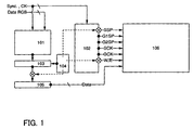
- the external controller portion has a frame memory 101, a timing controller 102, a first line buffer circuit 103, a second line buffer circuit 105 and a test circuit 104. These circuits generate various control signals to supply the generated various control signals to a display portion 106.
- the external controller portion is not limited to the aforementioned configuration and description of a power supply system such as a DC/DC converter is omitted.
- the frame memory 101 is a memory for holding a video signal which is required to display one frame while the line buffers 103 and 105 are memories for holding a video signal which is required to display one row.
- a time grayscale method is used as a driving method, therefore, one-row video signals related to a certain bit among video signals required to display one row is held in the line buffers.
- the video signal held in the line buffer at a time is not limited to be the aforementioned amount of data, and a configuration may be allowed in which more video signals are held to sequentially read as much data as necessary at a required timing.
- a reference clock signal (CK) As a signal used for driving the display device, there are a reference clock signal (CK), a synchronization signal (Sync), video signals for each of RGB (Data RGB). These signals are supplied from outside so that the reference clock signal (CK) and the synchronization signal (Sync) are inputted to the timing controller 102 to generate various control signals (in FIG 1, SSP, G1SP, G2SP, SCK, GCK, W/E and the like) which are required for driving the display device. Moreover, the reference clock signal (CK) is also used for timing controlling of writing/reading of the frame memory 101 and the like.
- video signals are written in the frame memory 101 which operates at a timing in accordance with the reference clock signal (CK), and rearranged in the frame memory 101 in the input order in accordance with the digital time grayscale method. Then, one-row video signals are read from the frame memory 101 to be transferred to the first line buffer circuit 103. At this time, the one-row video signals read from the frame memory 101 are tested by the test circuit 104 whether all the video signals of one row are video signals which display black. Herein, if a signal which displays white is included even for one dot, the video signals are transferred to the second line buffer circuit 105 and inputted to the display portion 106.
- CK reference clock signal
- the test circuit 104 outputs a control signal for stopping the input of a source driver start pulse (SSP) and a write erase selection signal (W/E signal) to the display portion 106, and a control signal for stopping the transfer of the video signal from the first line buffer circuit 103 to the second line buffer circuit 105. Therefore, the source driver in the display portion 106 does not perform the sampling operation of the row since no start pulse (SSP) is inputted to the shift register. Further, the video signal written in the second line buffer circuit 105 is also not changed from that of the previous row.
- SSP source driver start pulse
- W/E signal write erase selection signal
- FIG 2A shows a normal display timing.
- sampling pulses (Samp) 202 are sequentially outputted to perform a sampling of a video signal 203 in accordance with a timing at which the sampling pulses 202 are outputted.
- a sampling of video signals of an (n-1)th row is performed by the sampling pulses 202.
- a latch pulse (SLAT) 204 is inputted, the sampled video signals are simultaneously transferred to the second latch circuit.
- the second latch circuit outputs all the video signals of the (n - 1)th row (LAT2OUT).
- the video signal is outputted to the source signal line (SLine) while in a period in which the W/E signal is at Low level, the erasing signal is outputted, that is, the source signal line (SLine) is fixed at High level.
- the (n - 1)th row is selected (206) by the gate driver for writing 604 and the video signal is inputted to pixels of the (n - 1)th row.
- a (k - 1)th row is selected (207) by the gate driver for erasing 605 and the erasing signal is inputted to pixels of the (k - 1)th row.
- the aforementioned operations are repeated in the n-th row, an (n + 1)th row and later as well as a k-th row, a (k + 1)th row and later to complete the operation for one subframe.
- FIG 2B shows a state in which sampling operation is stopped in a certain row in accordance with the invention.
- a video signal is inputted to take the video signal in accordance with a sampling pulse. Therefore, in the source signal line (SLine), the video signal of the (n - 1)th row is outputted. Then, in the case where all the pixels of the n-th row and the (n + 1)th row display black, the output of the start pulse (SSP) and the video signal (Data) is forcibly stopped by the test circuit 104 so as not to perform the sampling operation. Therefore, the second latch circuit 608 continuously outputs the video signal of the (n - 1)th row (LAT2OUT).
- the W/E signal is also stopped by the test circuit 104 in that period to be fixed at Low level. Therefore, the video signal is not outputted to the source signal line (SLine) and the erasing signal is continuously inputted thereto. Gate signal lines of the (n-1)th row and the n-th row are brought into a selective state at a predetermined timing as usual so that an erasing signal at High level (equivalent to a black-display signal) outputted to the source signal line (SLine) is inputted to the pixel to display black.
- the start pulse (SSP) or the W/E signal is inputted at a predetermined timing, therefore, the sampling and the charging and discharging of the source signal line (SLine) are performed normally so that a predetermined video signal is inputted to each pixel to display a pattern.
- a source driver to perform a sampling of a video signal is a circuit with a high operating frequency in a display device, and effectively stopping unnecessary operation of the circuit greatly contributes to low power consumption.
- a white-display region is shown the most simple example in this embodiment mode, by using a similar test circuit, it is also possible to detect, for example, a white-display region and to stop sampling operation.
- a state in which a source signal line is fixed at Low level may be held.
- the source signal line is fixed at Low level in the first row.
- the W/E signal is fixed at High level so that the erasing signal is not inputted to the source signal line.
- a white-display signal that is, Low level signal may be continuously inputted from the source signal line which is fixed at Low level to pixels of a predetermined row.
- the W/E signal is described using only one system for simplicity, different systems are required for a W/E signal used for selection of writing or erasing operation of a source driver side, and a W/E signal used for the selection of a gate driver for writing or a gate driver for erasing.
- a way of supplying signals to the display portion is not limited especially. Signals may be externally inputted by a plurality of systems in advance or generated from one W/E signal.
- an organic EL display device is described as an example.
- the invention is not limited by an element which forms a pixel, and it is needless to say that the invention can be widely applied to a liquid crystal display device, a PDP, an FED and the like.
- the source driver has a shift register 301, a first latch circuit 302, a second latch circuit 303, a writing erasing selection circuit 304 and a buffer circuit 305.
- the shift register 301 outputs sampling pulses sequentially in accordance with clock signals (SCK, SCKb: SCKb is an inverted signal of SCK) and a start pulse (SSP).
- the first latch circuit 302 performs a sampling of a video signal (Data) in accordance with the sampling pulses outputted from the shift register 301. After completing the sampling of the video signal in all stages of the first latch circuit 302, when latch pulses (SLAT, SLATb: SLATb is an inverted signal of SLAT) are inputted, the video signals held in the first latch circuit 302 are simultaneously transferred to the second latch circuit 303.
- the writing erasing selection circuit 304 In the case where a W/E signal is active (herein, in the case of being at High level), the writing erasing selection circuit 304 inverts the video signal to output it. On the other hand, in the case where the W/E signal is at Low level, the write erase selection circuit 304 outputs a High level signal regardless of the video signal. Then, charge and discharge of source signal lines (SLine 1 to SLine n) are performed through the buffer circuit 305.
- the gate driver has a shift register 401 and a buffer circuit 402.
- the buffer circuit 402 uses a tri-state buffer using a W/E signal.
- the tri-state buffer functions as an inverter while in the case where the W/E signal is at Low level, the output of the tri-state buffer is in a floating state.
- the selection of the gate signal line is performed by a gate driver for writing and a gate driver for erasing in writing operation or erasing operation respectively, therefore, the tri-state buffer is provided so that selection operation of the gate signal line by one of the two gate drivers is not interrupted by the other.
- the shift register 401 outputs row selection pulses sequentially in accordance with clock signals (GCK, GCKb: GCKb is an inverted signal of GCK) and a start pulse (G1SP).
- the buffer circuit 402 is controlled by the W/E signal and the W/Eb signal (an inverted signal of W/E), and in the case where the W/E signal is active, the row selection pulse is inverted and sequentially outputted to gate signal lines (GLine 1 to GLine m). In the case where the W/E signal is at Low level, the output of the buffer circuit 402 is in a floating state.
- a gate driver for writing 412 and a gate driver for erasing 413 are positioned opposite to each other with a pixel portion 411 interposed therebetween (see FIG 4B). At this time, the W/E signal is outputted to one of the gate driver for writing 412 and the gate driver for erasing 413, an inverted signal of the W/E signal is outputted to the other thereof.
- the output of the tri-state buffer included in the other gate driver is in a floating state. Therefore, each other's selection operation of the gate signal line for writing or erasing is not interrupted.
- level shifter is not provided in the configuration of this embodiment, it may be provided appropriately if necessary.
- FIGS. 7 and 8A to 8F Shown as an example of the electronic apparatus here is a mobile phone which has housings 2700 and 2706, a panel 2701, a housing 2702, a printed wiring board 2703, an operation button 2704 and a battery 2705 (see FIG 7).
- the panel 2701 has a pixel portion in which a plurality of pixels are arranged in matrix.
- the panel 2701 is detachably mounted in the housing 2702 while the housing 2702 is attached to the printed wiring board 2703.
- the shape and size of the housing 2702 are changed appropriately in accordance with an electronic apparatus in which the panel 2701 is mounted.
- a plurality of semiconductor devices (also referred to as IC chips) which are packaged are mounted on the printed wiring board 2703.
- the plurality of semiconductor devices mounted on the printed wiring board 2703 are equivalent to a frame memory, a timing controller, a line buffer circuit, a test circuit, a central processing unit (CPU), a power supply circuit, an image processing circuit, a sound processing circuit, a transmit/receive circuit, a time detection circuit, a correction circuit, a temperature sensing circuit and the like, which are components of the display device of the invention.
- the panel 2701 is integrated with the printed wiring board 2703 through a connection film 2708.
- the panel 2701, the housing 2702 and the printed wiring board 2703 are put inside the housings 2700 and 2706, as well as the operation button 2704 and the battery 2705.
- the pixel portion included in the panel 2701 is arranged so as to be seen from an opening window provided in the housing 2700.
- housings 2700 and 2706 show one example of the exterior shape of mobile phones
- an electronic apparatus related to this embodiment can be changed to various modes in accordance with the function and application. Therefore, examples of modes of electronic apparatuses are described hereinafter with reference to FIGS. 8A to 8F.
- a mobile phone device includes a pixel portion 9102 and the like (see FIG 8A).
- a portable game device includes a pixel portion 9801 and the like (see FIG 8B).
- a digital video camera includes pixel portions 9701, 9702 and the like (see FIG 8C).
- a portable information terminal includes a pixel portion 9201 and the like (see FIG. 8D).
- a television device includes a pixel portion 9301 and the like (see FIG 8E).
- a monitor device includes a pixel portion 9401 and the like (see FIG 8F).
- the invention can be applied to various electronic apparatuses such as a television device (also referred to as a TV or a television receiver), a digital camera, a mobile phone set (also referred to as a mobile phone device or a mobile phone), a portable information terminal such as a PDA, a portable game device, a monitor device for computer (also referred to as a monitor), a sound reproducing device such as a car audio, and a home game device.
- Operation of a source driver can be stopped temporarily by applying the display device of the invention, and thus an electronic apparatus in which power consumption is reduced can be provided.
- the invention can stop operation of the source driver which consumes much power in the display device, leading to dramatic reduction in power consumption. Such an effect is very useful for electronic apparatuses such as portable terminals in which power consumption directly affects a continuous using time.
Landscapes
- Engineering & Computer Science (AREA)
- Physics & Mathematics (AREA)
- Computer Hardware Design (AREA)
- General Physics & Mathematics (AREA)
- Theoretical Computer Science (AREA)
- Chemical & Material Sciences (AREA)
- Crystallography & Structural Chemistry (AREA)
- Control Of Indicators Other Than Cathode Ray Tubes (AREA)
- Electroluminescent Light Sources (AREA)
Applications Claiming Priority (1)
| Application Number | Priority Date | Filing Date | Title |
|---|---|---|---|
| JP2004339682 | 2004-11-24 |
Publications (3)
| Publication Number | Publication Date |
|---|---|
| EP1662468A2 true EP1662468A2 (de) | 2006-05-31 |
| EP1662468A3 EP1662468A3 (de) | 2008-10-01 |
| EP1662468B1 EP1662468B1 (de) | 2017-10-25 |
Family
ID=35929933
Family Applications (1)
| Application Number | Title | Priority Date | Filing Date |
|---|---|---|---|
| EP05025577.7A Expired - Lifetime EP1662468B1 (de) | 2004-11-24 | 2005-11-23 | Oled anzeige mit aktiver matrix und elektronisches gerät |
Country Status (4)
| Country | Link |
|---|---|
| US (2) | US7932877B2 (de) |
| EP (1) | EP1662468B1 (de) |
| KR (1) | KR101167861B1 (de) |
| CN (1) | CN100485761C (de) |
Cited By (1)
| Publication number | Priority date | Publication date | Assignee | Title |
|---|---|---|---|---|
| US20090309860A1 (en) * | 2008-06-11 | 2009-12-17 | Chin-Hung Hsu | Driving Method and Related Device for Reducing Power Consumption of LCD |
Families Citing this family (16)
| Publication number | Priority date | Publication date | Assignee | Title |
|---|---|---|---|---|
| US9165505B2 (en) * | 2006-01-13 | 2015-10-20 | Semiconductor Energy Laboratory Co., Ltd. | Display device and electoric device having the same |
| EP1808844B1 (de) * | 2006-01-13 | 2012-10-31 | Semiconductor Energy Laboratory Co., Ltd. | Anzeigevorrichtung |
| KR101346858B1 (ko) * | 2008-11-12 | 2014-01-02 | 엘지디스플레이 주식회사 | 유기발광 표시장치 |
| KR101463651B1 (ko) * | 2011-10-12 | 2014-11-20 | 엘지디스플레이 주식회사 | 유기발광 표시장치 |
| GB2500401B (en) * | 2012-03-20 | 2020-06-03 | Ge Aviat Systems Ltd | Apparatus for an aircraft cockpit display |
| CA2808799A1 (en) * | 2012-03-20 | 2013-09-20 | Ge Aviation Systems Limited | Apparatus for an aircraft cockpit display |
| GB2501255B (en) | 2012-04-16 | 2018-04-11 | Ge Aviat Systems Ltd | Apparatus for aircraft dual channel display |
| GB2507524B (en) | 2012-11-01 | 2016-02-24 | Ge Aviat Systems Ltd | Apparatus for aircraft dual channel display |
| KR102166897B1 (ko) | 2014-02-11 | 2020-10-19 | 삼성디스플레이 주식회사 | 표시 장치 및 그 구동 방법 |
| WO2017138469A1 (ja) | 2016-02-10 | 2017-08-17 | シャープ株式会社 | アクティブマトリクス基板及び表示パネル |
| JP6957903B2 (ja) * | 2017-03-08 | 2021-11-02 | セイコーエプソン株式会社 | 表示装置及び電子機器 |
| CN106935219B (zh) * | 2017-03-31 | 2022-07-15 | 山东蓝贝易书信息科技有限公司 | 一种光能液晶书写板一键擦除控制电路系统 |
| KR101933929B1 (ko) * | 2017-05-23 | 2019-03-25 | 주식회사 라온텍 | 공간-시간 변조를 이용한 디스플레이 패널 및 이를 구동하는 디지털 화소 구동 방법 |
| JP6971078B2 (ja) * | 2017-08-01 | 2021-11-24 | シナプティクス・ジャパン合同会社 | 表示ドライバ及び表示装置 |
| US20200020271A1 (en) * | 2018-07-13 | 2020-01-16 | Innolux Corporation | Display device |
| CN113299244B (zh) * | 2021-05-24 | 2023-02-07 | 京东方科技集团股份有限公司 | 电压控制模组、驱动模组、驱动方法和显示装置 |
Citations (3)
| Publication number | Priority date | Publication date | Assignee | Title |
|---|---|---|---|---|
| JP2001005426A (ja) | 1999-06-23 | 2001-01-12 | Semiconductor Energy Lab Co Ltd | El表示装置及び電子装置 |
| JP2001324958A (ja) | 2000-03-10 | 2001-11-22 | Semiconductor Energy Lab Co Ltd | 電子装置およびその駆動方法 |
| JP2004339682A (ja) | 2003-05-12 | 2004-12-02 | Andritz Inc | 気相式と満液式の連続蒸解缶に用いるトップセパレーターおよび蒸解缶運転モードの転換方法 |
Family Cites Families (20)
| Publication number | Priority date | Publication date | Assignee | Title |
|---|---|---|---|---|
| US5233447A (en) | 1988-10-26 | 1993-08-03 | Canon Kabushiki Kaisha | Liquid crystal apparatus and display system |
| GB8909011D0 (en) | 1989-04-20 | 1989-06-07 | Friend Richard H | Electroluminescent devices |
| JP3476241B2 (ja) | 1994-02-25 | 2003-12-10 | 株式会社半導体エネルギー研究所 | アクティブマトリクス型表示装置の表示方法 |
| US20020024496A1 (en) | 1998-03-20 | 2002-02-28 | Hajime Akimoto | Image display device |
| JP3694527B2 (ja) | 1995-09-20 | 2005-09-14 | 株式会社 日立製作所 | 画像表示装置 |
| TW441136B (en) | 1997-01-28 | 2001-06-16 | Casio Computer Co Ltd | An electroluminescent display device and a driving method thereof |
| JP4092857B2 (ja) | 1999-06-17 | 2008-05-28 | ソニー株式会社 | 画像表示装置 |
| JP2001100710A (ja) | 1999-07-23 | 2001-04-13 | Seiko Epson Corp | 電気光学装置、その駆動方法、その走査線駆動回路および電子機器 |
| US7129918B2 (en) | 2000-03-10 | 2006-10-31 | Semiconductor Energy Laboratory Co., Ltd. | Electronic device and method of driving electronic device |
| JP4161511B2 (ja) | 2000-04-05 | 2008-10-08 | ソニー株式会社 | 表示装置およびその駆動方法並びに携帯端末 |
| JP3835113B2 (ja) | 2000-04-26 | 2006-10-18 | セイコーエプソン株式会社 | 電気光学パネルのデータ線駆動回路、その制御方法、電気光学装置、および電子機器 |
| WO2001091098A1 (en) | 2000-05-24 | 2001-11-29 | Hitachi, Ltd. | Color/black-and-white switchable portable terminal and display device |
| JP2002202881A (ja) | 2000-10-26 | 2002-07-19 | Matsushita Electric Ind Co Ltd | 画像表示装置 |
| JP2002204297A (ja) | 2000-11-02 | 2002-07-19 | Sharp Corp | 携帯情報機器 |
| JP2002169499A (ja) | 2000-11-30 | 2002-06-14 | Sanyo Electric Co Ltd | 表示パネルの駆動方法及び表示パネルの駆動制御装置 |
| JP2002328661A (ja) | 2001-04-27 | 2002-11-15 | Toshiba Corp | 液晶表示装置の駆動方法及び液晶表示装置 |
| JP2003015610A (ja) | 2001-06-29 | 2003-01-17 | Sanyo Electric Co Ltd | アクティブマトリクス型表示装置及びその制御装置 |
| JP2003058126A (ja) | 2001-08-17 | 2003-02-28 | Toshiba Corp | 表示装置及びその駆動方法 |
| CN1265346C (zh) | 2001-09-28 | 2006-07-19 | 索尼公司 | 显示存储器、驱动器电路、显示器和便携式信息设备 |
| JP2003316315A (ja) * | 2002-04-23 | 2003-11-07 | Tohoku Pioneer Corp | 発光表示パネルの駆動装置および駆動方法 |
-
2005
- 2005-11-17 US US11/280,727 patent/US7932877B2/en not_active Expired - Fee Related
- 2005-11-23 EP EP05025577.7A patent/EP1662468B1/de not_active Expired - Lifetime
- 2005-11-24 CN CNB2005101272447A patent/CN100485761C/zh not_active Expired - Fee Related
- 2005-11-24 KR KR1020050112945A patent/KR101167861B1/ko not_active Expired - Fee Related
-
2011
- 2011-04-13 US US13/085,522 patent/US8310433B2/en not_active Expired - Fee Related
Patent Citations (3)
| Publication number | Priority date | Publication date | Assignee | Title |
|---|---|---|---|---|
| JP2001005426A (ja) | 1999-06-23 | 2001-01-12 | Semiconductor Energy Lab Co Ltd | El表示装置及び電子装置 |
| JP2001324958A (ja) | 2000-03-10 | 2001-11-22 | Semiconductor Energy Lab Co Ltd | 電子装置およびその駆動方法 |
| JP2004339682A (ja) | 2003-05-12 | 2004-12-02 | Andritz Inc | 気相式と満液式の連続蒸解缶に用いるトップセパレーターおよび蒸解缶運転モードの転換方法 |
Cited By (2)
| Publication number | Priority date | Publication date | Assignee | Title |
|---|---|---|---|---|
| US20090309860A1 (en) * | 2008-06-11 | 2009-12-17 | Chin-Hung Hsu | Driving Method and Related Device for Reducing Power Consumption of LCD |
| US8878764B2 (en) * | 2008-06-11 | 2014-11-04 | Novatek Microelectronics Corp. | Driving method and related device for reducing power consumption of LCD by comparing received data |
Also Published As
| Publication number | Publication date |
|---|---|
| US8310433B2 (en) | 2012-11-13 |
| KR20060058044A (ko) | 2006-05-29 |
| US20060109215A1 (en) | 2006-05-25 |
| CN100485761C (zh) | 2009-05-06 |
| CN1783191A (zh) | 2006-06-07 |
| US20120062612A1 (en) | 2012-03-15 |
| KR101167861B1 (ko) | 2012-07-24 |
| EP1662468A3 (de) | 2008-10-01 |
| EP1662468B1 (de) | 2017-10-25 |
| US7932877B2 (en) | 2011-04-26 |
Similar Documents
| Publication | Publication Date | Title |
|---|---|---|
| US8310433B2 (en) | Display device and electronic apparatus | |
| US9035977B2 (en) | Display control drive device and display system | |
| EP1193675A2 (de) | Steuerverfahren für eine elektrooptische Vorrichtung, organische elektrolumineszierende Anzeigevorrichtung und elektronisches Gerät | |
| US20090009510A1 (en) | Data line driving circuit, display device and method of driving data line | |
| JP2004077567A (ja) | 表示装置及びその駆動方法 | |
| US7573454B2 (en) | Display driver and electro-optical device | |
| US7652645B2 (en) | Light emitting display | |
| JP4079873B2 (ja) | 表示装置用の駆動回路 | |
| US7551166B2 (en) | Display device, method for driving the same, and electronic device using the same | |
| EP1826741A2 (de) | Anzeigevorrichtung und elektronische Vorrichtung damit | |
| JP5116202B2 (ja) | 表示装置の駆動方法 | |
| EP1820180B1 (de) | Anzeigeeinrichtung und elektronische vorrichtung damit | |
| JP2004163919A (ja) | 表示装置及びその駆動方法並びに電子機器 | |
| JP4397576B2 (ja) | 表示装置の駆動方法 | |
| JP5235048B2 (ja) | 表示装置、電子機器 | |
| JP4128601B2 (ja) | 表示装置および表示装置の駆動方法 | |
| JP5008302B2 (ja) | 表示装置 | |
| JP5041777B2 (ja) | 表示装置及び電子機器 | |
| JP2005148085A (ja) | 表示装置及び表示装置の駆動方法並びに電子機器 | |
| JP2006146089A (ja) | 表示装置及び電子機器 |
Legal Events
| Date | Code | Title | Description |
|---|---|---|---|
| PUAI | Public reference made under article 153(3) epc to a published international application that has entered the european phase |
Free format text: ORIGINAL CODE: 0009012 |
|
| AK | Designated contracting states |
Kind code of ref document: A2 Designated state(s): AT BE BG CH CY CZ DE DK EE ES FI FR GB GR HU IE IS IT LI LT LU LV MC NL PL PT RO SE SI SK TR |
|
| AX | Request for extension of the european patent |
Extension state: AL BA HR MK YU |
|
| RIC1 | Information provided on ipc code assigned before grant |
Ipc: G09G 3/28 20060101AFI20060704BHEP |
|
| PUAL | Search report despatched |
Free format text: ORIGINAL CODE: 0009013 |
|
| AK | Designated contracting states |
Kind code of ref document: A3 Designated state(s): AT BE BG CH CY CZ DE DK EE ES FI FR GB GR HU IE IS IT LI LT LU LV MC NL PL PT RO SE SI SK TR |
|
| AX | Request for extension of the european patent |
Extension state: AL BA HR MK YU |
|
| RIC1 | Information provided on ipc code assigned before grant |
Ipc: G09G 3/32 20060101AFI20080822BHEP |
|
| 17P | Request for examination filed |
Effective date: 20090317 |
|
| AKX | Designation fees paid |
Designated state(s): DE FI FR GB NL |
|
| 17Q | First examination report despatched |
Effective date: 20100818 |
|
| GRAP | Despatch of communication of intention to grant a patent |
Free format text: ORIGINAL CODE: EPIDOSNIGR1 |
|
| INTG | Intention to grant announced |
Effective date: 20170303 |
|
| GRAJ | Information related to disapproval of communication of intention to grant by the applicant or resumption of examination proceedings by the epo deleted |
Free format text: ORIGINAL CODE: EPIDOSDIGR1 |
|
| INTC | Intention to grant announced (deleted) | ||
| GRAP | Despatch of communication of intention to grant a patent |
Free format text: ORIGINAL CODE: EPIDOSNIGR1 |
|
| INTG | Intention to grant announced |
Effective date: 20170731 |
|
| GRAS | Grant fee paid |
Free format text: ORIGINAL CODE: EPIDOSNIGR3 |
|
| GRAA | (expected) grant |
Free format text: ORIGINAL CODE: 0009210 |
|
| AK | Designated contracting states |
Kind code of ref document: B1 Designated state(s): DE FI FR GB NL |
|
| REG | Reference to a national code |
Ref country code: GB Ref legal event code: FG4D |
|
| REG | Reference to a national code |
Ref country code: DE Ref legal event code: R096 Ref document number: 602005052930 Country of ref document: DE |
|
| REG | Reference to a national code |
Ref country code: NL Ref legal event code: MP Effective date: 20171025 |
|
| PG25 | Lapsed in a contracting state [announced via postgrant information from national office to epo] |
Ref country code: NL Free format text: LAPSE BECAUSE OF FAILURE TO SUBMIT A TRANSLATION OF THE DESCRIPTION OR TO PAY THE FEE WITHIN THE PRESCRIBED TIME-LIMIT Effective date: 20171025 |
|
| PG25 | Lapsed in a contracting state [announced via postgrant information from national office to epo] |
Ref country code: FI Free format text: LAPSE BECAUSE OF FAILURE TO SUBMIT A TRANSLATION OF THE DESCRIPTION OR TO PAY THE FEE WITHIN THE PRESCRIBED TIME-LIMIT Effective date: 20171025 |
|
| REG | Reference to a national code |
Ref country code: DE Ref legal event code: R097 Ref document number: 602005052930 Country of ref document: DE |
|
| PLBE | No opposition filed within time limit |
Free format text: ORIGINAL CODE: 0009261 |
|
| REG | Reference to a national code |
Ref country code: FR Ref legal event code: ST Effective date: 20180731 |
|
| STAA | Information on the status of an ep patent application or granted ep patent |
Free format text: STATUS: NO OPPOSITION FILED WITHIN TIME LIMIT |
|
| GBPC | Gb: european patent ceased through non-payment of renewal fee |
Effective date: 20180125 |
|
| 26N | No opposition filed |
Effective date: 20180726 |
|
| PG25 | Lapsed in a contracting state [announced via postgrant information from national office to epo] |
Ref country code: FR Free format text: LAPSE BECAUSE OF NON-PAYMENT OF DUE FEES Effective date: 20171226 |
|
| PG25 | Lapsed in a contracting state [announced via postgrant information from national office to epo] |
Ref country code: GB Free format text: LAPSE BECAUSE OF NON-PAYMENT OF DUE FEES Effective date: 20180125 |
|
| PGFP | Annual fee paid to national office [announced via postgrant information from national office to epo] |
Ref country code: DE Payment date: 20201110 Year of fee payment: 16 |
|
| REG | Reference to a national code |
Ref country code: DE Ref legal event code: R119 Ref document number: 602005052930 Country of ref document: DE |
|
| PG25 | Lapsed in a contracting state [announced via postgrant information from national office to epo] |
Ref country code: DE Free format text: LAPSE BECAUSE OF NON-PAYMENT OF DUE FEES Effective date: 20220601 |