EP1650331A1 - Simulationsverfahren bezüglich der dichteverteilung und grössenverteilung von leerstellendefekt in einkristall und sauerstoffausscheidungskeim in einkristall - Google Patents
Simulationsverfahren bezüglich der dichteverteilung und grössenverteilung von leerstellendefekt in einkristall und sauerstoffausscheidungskeim in einkristall Download PDFInfo
- Publication number
- EP1650331A1 EP1650331A1 EP04734077A EP04734077A EP1650331A1 EP 1650331 A1 EP1650331 A1 EP 1650331A1 EP 04734077 A EP04734077 A EP 04734077A EP 04734077 A EP04734077 A EP 04734077A EP 1650331 A1 EP1650331 A1 EP 1650331A1
- Authority
- EP
- European Patent Office
- Prior art keywords
- single crystal
- distribution
- determining
- temperature
- melt
- Prior art date
- Legal status (The legal status is an assumption and is not a legal conclusion. Google has not performed a legal analysis and makes no representation as to the accuracy of the status listed.)
- Ceased
Links
- 239000013078 crystal Substances 0.000 title claims abstract description 282
- 238000009826 distribution Methods 0.000 title claims abstract description 154
- 239000011800 void material Substances 0.000 title claims abstract description 84
- 238000000034 method Methods 0.000 title claims abstract description 80
- 238000004088 simulation Methods 0.000 title claims abstract description 75
- 230000007547 defect Effects 0.000 title claims abstract description 44
- QVGXLLKOCUKJST-UHFFFAOYSA-N atomic oxygen Chemical compound [O] QVGXLLKOCUKJST-UHFFFAOYSA-N 0.000 title claims description 117
- 239000001301 oxygen Substances 0.000 title claims description 117
- 229910052760 oxygen Inorganic materials 0.000 title claims description 117
- 238000001556 precipitation Methods 0.000 title claims description 86
- 239000012528 membrane Substances 0.000 claims abstract description 98
- 238000001816 cooling Methods 0.000 claims abstract description 49
- 239000000155 melt Substances 0.000 claims abstract description 44
- 238000009792 diffusion process Methods 0.000 claims description 28
- 239000007788 liquid Substances 0.000 claims description 9
- 230000005855 radiation Effects 0.000 claims description 7
- 238000002844 melting Methods 0.000 claims description 6
- 230000008018 melting Effects 0.000 claims description 6
- 239000000376 reactant Substances 0.000 claims description 3
- 230000000694 effects Effects 0.000 abstract description 5
- 238000000926 separation method Methods 0.000 abstract 1
- XUIMIQQOPSSXEZ-UHFFFAOYSA-N Silicon Chemical compound [Si] XUIMIQQOPSSXEZ-UHFFFAOYSA-N 0.000 description 217
- 229910052710 silicon Inorganic materials 0.000 description 204
- 239000010703 silicon Substances 0.000 description 200
- 230000015572 biosynthetic process Effects 0.000 description 28
- VYPSYNLAJGMNEJ-UHFFFAOYSA-N silicon dioxide Inorganic materials O=[Si]=O VYPSYNLAJGMNEJ-UHFFFAOYSA-N 0.000 description 15
- 230000004907 flux Effects 0.000 description 13
- 230000000052 comparative effect Effects 0.000 description 12
- 239000010453 quartz Substances 0.000 description 10
- 125000004430 oxygen atom Chemical group O* 0.000 description 7
- 125000004429 atom Chemical group 0.000 description 5
- 238000004458 analytical method Methods 0.000 description 4
- 238000005259 measurement Methods 0.000 description 4
- 238000006243 chemical reaction Methods 0.000 description 3
- 238000004519 manufacturing process Methods 0.000 description 3
- 239000011159 matrix material Substances 0.000 description 3
- 229910052814 silicon oxide Inorganic materials 0.000 description 3
- 239000007787 solid Substances 0.000 description 3
- OKTJSMMVPCPJKN-UHFFFAOYSA-N Carbon Chemical compound [C] OKTJSMMVPCPJKN-UHFFFAOYSA-N 0.000 description 2
- 230000004913 activation Effects 0.000 description 2
- 229910052681 coesite Inorganic materials 0.000 description 2
- 238000007796 conventional method Methods 0.000 description 2
- 229910052906 cristobalite Inorganic materials 0.000 description 2
- 230000001419 dependent effect Effects 0.000 description 2
- 238000001514 detection method Methods 0.000 description 2
- 238000011156 evaluation Methods 0.000 description 2
- 229910002804 graphite Inorganic materials 0.000 description 2
- 239000010439 graphite Substances 0.000 description 2
- 238000010438 heat treatment Methods 0.000 description 2
- 238000000329 molecular dynamics simulation Methods 0.000 description 2
- 239000000377 silicon dioxide Substances 0.000 description 2
- LIVNPJMFVYWSIS-UHFFFAOYSA-N silicon monoxide Chemical compound [Si-]#[O+] LIVNPJMFVYWSIS-UHFFFAOYSA-N 0.000 description 2
- 229910001220 stainless steel Inorganic materials 0.000 description 2
- 239000010935 stainless steel Substances 0.000 description 2
- 229910052682 stishovite Inorganic materials 0.000 description 2
- 238000003860 storage Methods 0.000 description 2
- 229910052905 tridymite Inorganic materials 0.000 description 2
- 229910001218 Gallium arsenide Inorganic materials 0.000 description 1
- 238000013459 approach Methods 0.000 description 1
- 230000004888 barrier function Effects 0.000 description 1
- 238000004364 calculation method Methods 0.000 description 1
- 238000013461 design Methods 0.000 description 1
- 238000010586 diagram Methods 0.000 description 1
- 239000007789 gas Substances 0.000 description 1
- 238000000386 microscopy Methods 0.000 description 1
- 230000003287 optical effect Effects 0.000 description 1
- 239000002245 particle Substances 0.000 description 1
- 230000006798 recombination Effects 0.000 description 1
- 238000005215 recombination Methods 0.000 description 1
- SBIBMFFZSBJNJF-UHFFFAOYSA-N selenium;zinc Chemical compound [Se]=[Zn] SBIBMFFZSBJNJF-UHFFFAOYSA-N 0.000 description 1
- 239000000126 substance Substances 0.000 description 1
- 238000012360 testing method Methods 0.000 description 1
Images






Classifications
-
- C—CHEMISTRY; METALLURGY
- C30—CRYSTAL GROWTH
- C30B—SINGLE-CRYSTAL GROWTH; UNIDIRECTIONAL SOLIDIFICATION OF EUTECTIC MATERIAL OR UNIDIRECTIONAL DEMIXING OF EUTECTOID MATERIAL; REFINING BY ZONE-MELTING OF MATERIAL; PRODUCTION OF A HOMOGENEOUS POLYCRYSTALLINE MATERIAL WITH DEFINED STRUCTURE; SINGLE CRYSTALS OR HOMOGENEOUS POLYCRYSTALLINE MATERIAL WITH DEFINED STRUCTURE; AFTER-TREATMENT OF SINGLE CRYSTALS OR A HOMOGENEOUS POLYCRYSTALLINE MATERIAL WITH DEFINED STRUCTURE; APPARATUS THEREFOR
- C30B15/00—Single-crystal growth by pulling from a melt, e.g. Czochralski method
- C30B15/20—Controlling or regulating
-
- C—CHEMISTRY; METALLURGY
- C30—CRYSTAL GROWTH
- C30B—SINGLE-CRYSTAL GROWTH; UNIDIRECTIONAL SOLIDIFICATION OF EUTECTIC MATERIAL OR UNIDIRECTIONAL DEMIXING OF EUTECTOID MATERIAL; REFINING BY ZONE-MELTING OF MATERIAL; PRODUCTION OF A HOMOGENEOUS POLYCRYSTALLINE MATERIAL WITH DEFINED STRUCTURE; SINGLE CRYSTALS OR HOMOGENEOUS POLYCRYSTALLINE MATERIAL WITH DEFINED STRUCTURE; AFTER-TREATMENT OF SINGLE CRYSTALS OR A HOMOGENEOUS POLYCRYSTALLINE MATERIAL WITH DEFINED STRUCTURE; APPARATUS THEREFOR
- C30B29/00—Single crystals or homogeneous polycrystalline material with defined structure characterised by the material or by their shape
- C30B29/02—Elements
- C30B29/06—Silicon
-
- C—CHEMISTRY; METALLURGY
- C30—CRYSTAL GROWTH
- C30B—SINGLE-CRYSTAL GROWTH; UNIDIRECTIONAL SOLIDIFICATION OF EUTECTIC MATERIAL OR UNIDIRECTIONAL DEMIXING OF EUTECTOID MATERIAL; REFINING BY ZONE-MELTING OF MATERIAL; PRODUCTION OF A HOMOGENEOUS POLYCRYSTALLINE MATERIAL WITH DEFINED STRUCTURE; SINGLE CRYSTALS OR HOMOGENEOUS POLYCRYSTALLINE MATERIAL WITH DEFINED STRUCTURE; AFTER-TREATMENT OF SINGLE CRYSTALS OR A HOMOGENEOUS POLYCRYSTALLINE MATERIAL WITH DEFINED STRUCTURE; APPARATUS THEREFOR
- C30B15/00—Single-crystal growth by pulling from a melt, e.g. Czochralski method
- C30B15/20—Controlling or regulating
- C30B15/206—Controlling or regulating the thermal history of growing the ingot
-
- Y—GENERAL TAGGING OF NEW TECHNOLOGICAL DEVELOPMENTS; GENERAL TAGGING OF CROSS-SECTIONAL TECHNOLOGIES SPANNING OVER SEVERAL SECTIONS OF THE IPC; TECHNICAL SUBJECTS COVERED BY FORMER USPC CROSS-REFERENCE ART COLLECTIONS [XRACs] AND DIGESTS
- Y10—TECHNICAL SUBJECTS COVERED BY FORMER USPC
- Y10T—TECHNICAL SUBJECTS COVERED BY FORMER US CLASSIFICATION
- Y10T117/00—Single-crystal, oriented-crystal, and epitaxy growth processes; non-coating apparatus therefor
- Y10T117/10—Apparatus
- Y10T117/1004—Apparatus with means for measuring, testing, or sensing
- Y10T117/1008—Apparatus with means for measuring, testing, or sensing with responsive control means
Definitions
- the present invention relates to a computer-based simulation for predicting the distribution of densities and sizes of grow-in defects and oxygen precipitation nuclei developed within a single crystal of a substance such as silicon during its formation like the one pulled up from a crucible according to the Czochralski method (CZ method hereinafter).
- CZ method Czochralski method
- the term "grow-in defect” used herein refers to a void defect comprising a void and an inner wall oxide membrane, and includes, for example, crystal originated particles (COP hereinafter), which may be observed on the surface of a wafer, and laser scattering tomograph defects (LSTD), which may be observed in the structure of the crystal itself.
- COP crystal originated particles
- LSTD laser scattering tomograph defects
- the oxygen precipitation nucleus refers to a nucleus formed as a result of the consumption of oxygen in air holes within the structure of a single crystal.
- a comparatively low temperature 700 to 800°C
- a higher temperature 1000 to 1100°C
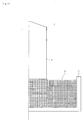
- a method which consists of applying an overall heat conduction simulation to a silicon single crystal 4 pulled up from a pulling-up machine 1 according to the CZ method as shown in Fig. 11.
- the method comprises the steps of predicting the distribution of temperatures within a silicon melt 2 by working on the heat conductivity of silicon melt 2 making allowance for the structural elements of a hot zone of the pulling-up machine 1 and the pulling-up speed of silicon single crystal 4, applying a mesh over the silicon single crystal 4 and determining, for each mesh, its coordinates and temperature from the internal temperature distribution, and solving a diffusion equation based on the diffusion coefficients of silicon atoms and air holes within an inter-lattice space of silicon single crystal 4 and boundary conditions using a computer, thereby determining the distribution of silicon atoms and air holes in the inter-lattice space.
- members constituting the hot zone are covered with a mesh for modeling. What is noteworthy is that each of the mesh applied to silicon melt 2 has a rather gross area or
- a method for producing a silicon single crystal by the CZ method has- also been known which consists of feeding, as input, the operation condition of the machine and temperature distribution within the crucible to a computer, thereby allowing the computer to predict, by simulation, the sizes and densities of grow-in defects due to air holes which might develop in the single crystal at the given growth speed of crystal based on a known relationship, and adjusting, based on the above simulation result, the machine such that the growth speed of crystal is kept at a specified level so as to make the sizes and densities of grow-in defects which might develop within the single crystal during its formation equal to or below predetermined thresholds (see, for example, Patent literature 1).
- Patent literature 1 Japanese Unexamined Patent Application Publication No. 2002-145696
- the above conventional method for predicting, by simulation, the distribution of densities of inter-lattice silicon atoms and air holes has the following problems: it.ignores convection currents which exist in a real silicon melt worked by a pulling-up machine; the mesh applied to a silicon melt is rather coarse, and thus reproducibility of the shape of solid-liquid interface is so degraded as to disable the precise prediction of the temperature distribution within a single crystal.
- the distribution of densities of inter-lattice silicon atoms and air holes in a silicon single crystal predicted by this method may considerably diverge from the result actually obtained by measurement.
- a first object of the present invention is to provide a simulation method for predicting the distribution of densities and sizes of void defects in a single crystal, the method enabling a precise prediction of the distribution of densities and sizes of void defects constituted of voids and inner wall oxide membranes within a single crystal by analyzing the temperature distribution within the single crystal while it is growing with a due consideration paid to the convention currents existent in a melt, and then by analyzing the cooling process to which the single crystal will be subjected after the single crystal is separated from the melt.
- a second object of the present invention is to provide a simulation method for predicting the distribution of densities and sizes of oxygen precipitation nuclei in a single crystal, the method enabling a precise prediction of the distribution of densities and sizes of oxygen precipitation nuclei within a single crystal by analyzing the temperature distribution within the single crystal while it is growing with a due consideration paid to the convection currents existent in a melt, and then by analyzing the cooling process to which the single crystal will be subjected after the single crystal is separated from the melt.
- an aspect of the invention described in Claim 1 relates to a computer-based simulation method for predicting the distribution of densities and sizes of void defects in a single crystal, the method comprising: a first step of applying a mesh onto each member in-a hot zone of a pulling-up machine 11 for modeling from the start of pulling up a single crystal 14 from a melt 12 by the pulling-up machine 11 to the completion of cooling the single crystal 14; a second step of classifying mesh points according to individual members of the hot zone, assigning to mesh points classified to a given member a property value peculiar to the member, determining the pulled-up length of the single crystal 14 at a given time, and the pulling-up speed of the single crystal 14 at that time, and sending the data to a computer; a third step of determining the distribution of temperatures over the surface of the members of hot zone based on the heat amount generated by a heater and the radiation rate of the members; a fourth step of determining the distribution of internal temperatures of the members of hot zone by solving
- FIG. 5 to 10 another aspect of the invention described in Claim 2 relates to a computer-based simulation method for predicting the distribution of densities and sizes of oxygen precipitation nuclei in a single crystal, the method comprising: a first step of applying a mesh onto each member in a hot zone of a pulling-up machine 11 for modeling from the start of pulling up a single crystal 14 from a melt 12 by the pulling-up machine 11 to the completion of cooling the single crystal 14; a second step of classifying mesh points according to individual members and reactants of the hot zone, assigning to mesh points classified to a given member a property value peculiar to the member, determining the pulled-up length of the single crystal 14 at a given time, and the pulling-up speed of the single crystal 14 at that time, and sending the data to a computer; a third step of determining the distribution of temperatures over the surface of the members based on the heat amount generated by a heater and the radiation rate of the members; a fourth step of determining the distribution of internal temperatures of the members of hot
- the method determines the distribution of densities and sizes of void defects comprising voids 21 and inner wall oxide membranes 22 within a single crystal 14 with due consideration paid to the effect of slow and rapid cooling during the cooling process to which the single crystal 14 is subjected after it is separated from melt 12, determines the incidence per unit time of oxygen precipitation nuclei and their critical radius, terminates, when the per-unit-time incidence of oxygen precipitation nuclei exceeds zero, computation for determining the radius of voids and thickness of inner wall oxide membrane 22, and determines instead the radius of oxygen precipitation nuclei.
- the method thus allows a precise prediction of the distribution of densities and sizes of oxygen precipitation nuclei within a single crystal 14.
- the critical radius of an oxygen precipitation nucleus mentioned herein refers to the minimum radius of an oxygen precipitation nucleus developed during the growth of a crystal. The critical radius is determined dependent on the oversaturated density of air holes and oversaturated density of oxygen.
- the inventive method determines with the aid of a computer not only the distribution of temperatures within a single crystal growing from a melt with due consideration paid to convection currents in the melt, but also the distribution of temperatures in the single crystal during the cooling process, specially, with due consideration of the effect of slow and rapid cooling during the cooling process of the single crystal separated from the melt, and determines the distribution of voids in the single crystal using a computer, and then relates the radius of void with the thickness of inner wall oxide membrane formed around the void using a computer. Accordingly, it is possible to precisely predict the distribution of densities and sizes of void defects comprising voids and inner wall oxgen membranes in a single crystal.
- the method makes it possible to precisely predict the distribution of densities and sizes of oxygen precipitation nuclei in a single crystal by determining not only the distribution of temperatures within a single crystal growing from a melt with convection currents of the melt considered with using a computer, but also the distribution of temperatures within the single crystal during a cooling process.
- the method determines the distribution of densities and sizes of void defects comprising voids and inner wall oxide membranes, and determines the incidence per unit time of oxygen precipitation nuclei and the critical radius of those nuclei, terminates, when the per-unit-time incidence of oxygen precipitation nuclei exceeds zero, computation for determining the radius of voids and thickness of inner wall oxide membrane, and determines the radius of oxygen precipitation nuclei using the computer.
- a quartz crucible 13 for storing a silicon melt 12.
- the quartz crucible 13 is connected via a graphite susceptor and supporting axis (not shown) to a crucible moving means which moves the quartz crucible 13 upward or downward while rotating it.
- a heater (not shown) by a specified distance apart from the quartz crucible 13.
- the heater is surrounded by a heat-insulating cylinder (not shown). The heater heats a highly pure silicon polycrystal put into quartz crucible 13 to turn it into a silicon melt 12.
- Onto the upper end of the chamber a cylindrical casing (not shown) is joined, and the pulling-up means is attached to the casing.
- the pulling-up machine is so designed as to pull up a silicon single crystal 14 while rotating it.
- the simulation system applies a mesh onto each member in a hot zone of a silicon single crystal pulling-up machine 11 for modeling, where a silicon single crystal 14 having a specified length L 1 (e.g., 100 mm) is pulled up, such as the chamber, quartz crucible 13, silicon melt 12, silicon single crystal 14, graphite susceptor, and heat-insulating cylinder for modeling. More specifically, for each member in the hot zone, the coordinates of relevant mesh points are fed to a computer.
- L 1 e.g. 100 mm
- those arranged in the transverse direction of the silicon single crystal 14 and totally or partially beneath the silicon single crystal 14 has a size of 0.01 to 5.00 mm, more preferably 0.25 to 1.00 mm.
- those arranged in the longitudinal direction of the silicon single crystal 14 and totally or partially separated from the silicon single crystal 14 has a size of 0.01 to 5.00 mm, more preferably 0.1 to 0.5 mm.
- the transverse mesh is set to have a size of 0.01 to 5.00 mm. This is because if the lower limit is below 0.01 mm, computation will require an undue long time and if the upper limit is over 5.00 mm, computation will become so unstable that it can not give a definitive answer for the shape of solid-liquid interface even when repeated as desired.
- the longitudinal mesh is set to have a size of 0.01 to 5.00 mm. This is because if the lower limit is below 0.01 mm, computation will require an undue long time and if the upper limit is over 5.00 mm, computation will give an answer divergent from the one obtained by measurement as to the shape of solid-liquid interface.
- the mesh beneath the silicon single crystal 14 should be preferably selected to have that size limit. If it is necessary to apply the above size limit of 0.01 to 5.00 mm to a certain fraction of longitudinal mesh, the mesh of silicon melt 12 at the surface of melt or at the bottom surface of crucible should be preferably selected to have that size limit.
- the simulation system classifies the mesh points according to individual members and reactants of the hot zone, assigns to mesh points classified to a given member a property value peculiar to the member, and sends the data to a computer.
- the simulation system assigns, to each mesh point related with the chamber, heat conductivity, radiation rate, viscosity, thermal expansion coefficient, density, specific heat capacity, etc. of stainless steel, and sends the data to a computer.
- the simulation system delivers to the computer data such as the pulled-up length of silicon single crystal 14 at a given time, pulling-up speed of silicon single crystal 14 at that time, and eddy current parameter C obtained from eddy current model equation (1) described below.
- the simulation system determines, with the aid of the computer, the distribution of temperatures over the surface of the members of hot zone based on the heat amount generated by the heater and the radiation rate of the members.
- the simulation system sets a desired heat amount and feeds it to the computer, and instructs the computer to determine the distribution of temperatures over the surface of the members based on that heat amount generated by the heater and the radiation rate of the members.
- the simulation system solves, with the aid of the computer, heat conduction equation (1) based on the distribution of temperatures over the surface of the members of hot zone and the heat conductivities of those members, thereby determining the distribution of internal temperatures of the members.
- the equation is written on the assumption that the pulling-up machine is placed in an XYZ orthogonal coordinate system. In reality, however, computation is performed on the assumption that the pulling-up machine is placed in a polar coordinate system.
- ⁇ represents the density of a member, c the specific heat capacity of the member, T the absolute temperature of a given mesh point in the member, and t time.
- ⁇ x , ⁇ y and ⁇ z represent the x-, y- and z-components of the heat conductivity of the member, respectively, and q heat amount generated by the heater.
- the simulation system also obtains the distribution of temperatures within silicon melt 12 by means of the heat conduction equation (1) described above, and determines, with the aid of the computer, the distribution of flow velocities within silicon melt 12 based on the distribution of internal temperatures thereof, by solving eddy current model equation (2) in conjunction with Navier-Stokes equations (3) to (5) assuming that the silicon melt 12 includes eddy currents.
- K t represents the heat conductivity of eddy currents of silicon melt 12
- c the specific heat capacity of silicon melt 12
- Pr t the Prandtl number
- ⁇ the density of silicon melt 12
- C eddy current parameter the distance from the wall of quartz crucible 13 storing silicon melt 12
- k the root mean square of variable components relative to the average flow velocity of silicon melt 12.
- u, v and w represent the x-, y- and z-components of the flow velocity of a given mesh point in silicon melt 12 respectively, ⁇ 1 the molecular dynamic viscosity index (property value) of silicon melt 12, ⁇ t the molecular dynamic viscosity index due to the eddy currents of silicon melt 12, and F x , F y and F z the x-, y-, and z-components of the volume force acting on silicon melt 12.
- the eddy current model equation (2) is also called the kl-model equation, and any desired number between 0.4 and 0.6 is preferably chosen as the eddy current parameter of this model equation.
- the simulation system performs a renewed calculation with the aid of the computer using the distribution of internal temperatures of silicon melt 12 determined as described below, and determines again the distribution of internal temperatures of silicon melt 12 by solving the heat energy equation (6) below with consideration being paid now to the convection currents within the silicon melt 12.
- u, v and w represent the x-, y- and z-components of the flow velocity of a given mesh point in silicon melt 12 respectively
- T the absolute temperature of the mesh point
- ⁇ the density of silicon melt 12
- c the specific heat capacity of silicon melt 12
- K 1 its molecular heat conductivity
- K t the heat conductivity of eddy currents obtained from equation (1).
- the simulation system determines, with the aid of the computer, the shape of the solid-liquid interface between silicon single crystal 14 and silicon melt 12 based on isothermal lines including a tri-junction S (tri-junction at which solid, liquid and gas coexist) shown in Fig. 5.
- the simulation system alters (increases gradually) the heat amount generated by the heater to be fed to the computer.
- the simulation system repeats steps 3 to 5 until the tri-junction S is heated up to the melting point of silicon single crystal 14. Then, the simulation system determines the distribution of temperatures within the pulling-up machine 11, and seeks, for each mesh point of silicon single crystal, its coordinates and temperature. The data is fed to the computer for storage.
- the simulation system allows the silicon single crystal 14 to be pulled up further by ⁇ (e.g., 50 mm) in addition to the length L 1 .
- the simulation system repeats steps 1 to 6, determines the distribution of temperatures within the pulling-up machine 11, and seeks, for each mesh point of silicon single crystal 14, its coordinates and temperature.
- the data is fed to the computer for storage.
- Operation at the seventh step starts when silicon single crystal 14 is elongated from L 1 to L 2 (L 2 is a length at which the silicon single crystal 14 is separated from silicon melt 12 (length of the single crystal when its growth is stopped)), and separated from silicon melt 12, and continues while the silicon single crystal 12 is further pulled up so that its height is extended from H 1 (H 1 is the distance from the shoulder of the straight body of silicon single crystal 14 to the surface of silicon melt 12 (Fig. 5)) to H 2 (H 2 is the distance from the shoulder of the straight body of silicon single crystal 14 to the surface of silicon melt 12 when cooling process is completed), that is, up to the time when the cooling of silicon single crystal is completed.
- the simulation system allows silicon single crystal 14 to be pulled up further by ⁇ (e.g., 50 mm), and repeats steps 1 to 6 as described above.
- step 8 the simulation system divides the period t from a time to when silicon single crystal 14 is pulled up from silicon melt 12 to a time t 1 when silicon single crystal 14 is separated from silicon melt 12 and has undergone cooling process at specified intervals or ⁇ t seconds (brief time intervals). At that time, the simulation system also feeds data such as the diffusion coefficients and boundary conditions of inter-lattice silicon atoms and air holes within silicon single crystal 14 and constants to be entered into the equations used for the computation of the distribution of densities and sizes of voids 21 and inner wall oxide membrane 22 (Fig. 6) to the computer.
- the simulation system gathers, for each mesh point of silicon single crystal 14, its coordinates and temperature obtained at step 7 for each interval ⁇ t, and determines the distribution of internal temperatures of silicon single crystal 14 in terms of the pulled-up length L 1 and pulled-up height H 1 of silicon single crystal 14.
- the simulation system determines for each mesh point of silicon single crystal 14 its coordinates and temperature at every incremental length ⁇ at steps 1 to 7. Provided that the pulled-up length L 1 and pulled-up height H 1 of silicon single crystal 14 are reached ⁇ t sec after t 0 , the simulation system determines the distribution of internal temperatures of silicon single crystal 14 at that time interval. Next, the simulation system determines the distribution of densities of air holes and inter-lattice atoms within silicon single crystal 14 accumulated during the time elapsed up to ⁇ t sec by solving the diffusion equation based on the diffusion coefficients of air holes and inter-lattice silicon atoms in silicon single crystal 14 and their boundary conditions (ninth step).
- equation necessary for computing the density C v of air holes is represented by equation (7) below
- equation necessary for computing the density C i of inter-lattice silicon atoms is represented by equation (8) below.
- equations (7) and (8) it is assumed that thermal equilibrium among air holes and among inter-lattice silicon atoms is maintained all over the surface of the silicon single crystal, in order to facilitate the computation of density C v and density C i over time.
- K 1 and K 2 are constants, E i and E v formation energy of inter-lattice silicon atoms and air holes respectively, C ve and C ie equilibrium densities of air holes and inter-lattice silicon atoms respectively, K B Boltzman's constant, and T absolute temperature.
- the above equilibrium equations can be made differentials over time, to give following equations (9) and (10) for air holes and inter-lattice silicon atoms respectively.
- T p represents the temperature at which the inner wall oxide membrane 22 (silicon oxide (SiO x ) membrane developed on the surface of void 21) starts to form.
- T v represents the temperature at which void 2firstarts to form (Fig. 6).
- the first term of the right hand side of equations (9) and (10) is the same with the Fick's diffusion equation.
- D v and D i in the first term represent the diffusion coefficients of air holes and inter-lattice silicon atoms respectively which are represented by following equations (11) and (12).
- Equations (11) and (12) ⁇ E v and ⁇ E i represent activation energies of air holes and inter-lattice silicon atoms, d v and d i constants peculiar to voids and inter-lattice silicon atoms respectively.
- E v t and E i t in the second term of the right hand side of equations (9) and (10) represent activation energies of air holes and inter-lattice silicon atoms respectively.
- k iv in the third term of the right hand side of equations (9) and (10) represents a recombination constant of air holes as well as of inter-lattice silicon pairs.
- N v in the fourth term of the right hand side of equations (9) and (10) represents the density of voids 21, and r v in the same term represents the radius of voids 21.
- N p in the fifth term of the right hand side of equation (9) represents the density of inner wall oxide membrane 22, and R P in the same term the outer radius of inner wall oxide membrane 22.
- Equation (9) applies for the case where each flux of air holes responsible for the precipitation of air holes is sufficiently large, and the difference in volume per unit mass between Si matrix and SiO x constituting inner wall oxide membrane both contributing to the formation of silicon single crystal 14 can be accounted for by voids, that is, ⁇ D 0 C 0 ⁇ D v (C v -C ve ).
- ⁇ represents the consumed fraction of an air hole for one oxygen atom
- D 0 the diffusion coefficient of oxygen
- C 0 the density of oxygen.
- T p represents the temperature at which the inner wall oxide membrane 22 starts to form.
- T v represents the temperature at which void 2firstarts to form.
- the first term of the right hand side of equation (13) is the same with the Fick's diffusion equation.
- D v in the first term represents the diffusion coefficients of air holes which are represented by equation (11). Then, at step 10, the simulation system determines the temperature T v at which voids 2firstart to form by solving equation (14) below based on the distribution of densities C v of air holes obtained from the above diffusion equation.
- C v represents the density of air holes in silicon single crystal 14, C v0 the equilibrium density of air holes at the melting point T m of silicon single crystal 14, and E v the formation energy of air holes.
- ⁇ v represents the interface energy of silicon single crystal 14 at a crystal surface (111), ⁇ the density of silicon single crystal 14, and k B Boltzman constant.
- the simulation system determines the density N v of voids 21 using approximation (15) below observed when the temperature is gradually lowered until it becomes equal to or below the void formation temperature T v .
- n represents the density of voids 21, and (dT/dt) the cooling speed of silicon single crystal 14.
- D v represents the diffusion coefficient of voids 21, k B Boltzman constant, and C v the density of air holes in silicon single crystal 14.
- the simulation system determines, for each qmesh point of silicon single crystal 14, the radius r v of voids when the temperature is below the void formation temperature T v by means of equation (16) below.
- the growth speed of voids 21 depends on the diffusion speed of air holes. It should be noted further that, although the void has an octahedron form in reality, the equation assumes that the void has a spherical form.
- t1 represents the time at which the temperature of a given mesh point of silicon single crystal 14 is down to the void formation temperature T v .
- r ver represents the critical radius of void 21.
- the critical radius of void r ver is equal to the radius of voids 21 observed at time t1.
- C ve and C ie represent the equilibrium densities of air holes and inter-lattice silicon atoms respectively.
- the simulation system determines the temperature at which an inner wall oxide membrane 22 starts to grow around a void 21. If the temperature Tp of formation of inner wall oxide membrane 22 is lower than the temperature T v of formation of voids 21, oxygen binds to air hole, and oxide membrane 22 grows on the internal wall of the void 21 (Fig. 6).
- oxide membrane 22 grows soon after the formation of a void 21.
- the term "soon” used here means a "time interval between the formation of the void and the next round of computation.” Accordingly, the temperature T p of formation of inner wall oxide membrane 22 is the same with the temperature T v of void formation.
- the simulation system determines the radius r v of voids 21 and the thickness d of inner wall oxide membrane 22 when the temperature is lowered below the membrane formation temperature T p , and relates the radius r v of void 21 with the thickness d of inner wall oxide membrane 22.
- oxygen diffuses and reacts with silicon to form a membrane 22 over the internal wall of a void. Assume oxygen approaches from outside an inner wall oxide membrane 22 having a radius of R P with the center of the sphere being at the original point of a coordinate system. Then, the flux J 0 of oxygen can be obtained from equation (17) below.
- D 0 represents the diffusion coefficient of oxygen, C 0 the density of oxygen, C 0eif the equilibrium density of oxygen in a spherical void 21 having a radius of R P with its center correspondent with the original point of a coordinate system, and g 0 the fraction of oxygen atoms involved in reaction at the interface between SiO x and Si on the external surface of the sphere, that is, at the outer surface of inner wall oxide membrane 22 there.
- the flux J v of air holes flowing from outside into the outer surface of inner wall oxide membrane 22 (surface of a sphere having a radius R P ) can be determined by means of equation (18) below.
- g v represents the fraction of air holes involved in reaction at the outer surface of inner wall oxide membrane 22, and C veif the equilibrium density of air holes at the outer surface of inner wall oxide membrane 22.
- C veif the equilibrium density of air holes at the outer surface of inner wall oxide membrane 22.
- the fraction of an air hole consumed by an oxygen atom is ⁇ . If a void has a flux of ⁇ J 0 with respect to the flux J 0 of oxygen, then inner wall oxide membrane 22 will grow smoothly with no distortion. Then, the flux ⁇ J 0 of a void can be determined from equation (19) below.
- (Jv - ⁇ J 0 ) represents the flux of air holes absorbed by inner wall oxide membrane 22. If the flux of air holes from outside to inner wall oxide membrane 22 increases ((Jv - ⁇ J 0 ) > 0), or if the flux of air holes from inside the void to inner wall oxide membrane 22 over time increases ((Jv - ⁇ J 0 ) ⁇ 0), and the fraction of variations of flux over time is ⁇ , ⁇ will be determined by the thickness of inner wall oxide membrane 22. If inner wall oxide membrane 22 has a thickness d, that is, (R P - r v ) ⁇ do, inner wall oxide membrane 22 will receive air holes from inside the void as well as from outside.
- equation (20) will be obtained.
- r v represents the radius of void 21 obtained from equation (16)
- R P the outer radius of inner wall oxide membrane 22.
- D 0 represents the diffusion coefficient of oxygen
- C 0 the density of oxygen.
- equation (21) Since the number of SiO x molecules constituting inner wall oxide membrane 22 varies depending on the consumption of the flux J 0 of oxygen coming from outside to the inner wall oxide membrane 22 which is determined by equation (20), equation (21) below will be obtained.
- ⁇ is a constant correspondent with x of SiO x .
- equation (21) When equation (21) is entered into equation (20), equation (22) below is obtained.
- equation (22) ⁇ is ⁇ SiOx / ⁇ Si .
- ⁇ si In this definition of ⁇ , ⁇ si is 1/ ⁇ , and ⁇ represents the density of silicon single crystal 14.
- the simulation system repeats steps 8 to steps 14 described above until the cooling of silicon single crystal is completed (step 15). For this purpose, the simulation system uses equations (9) to (24) interchangeably with each other with the aid of the computer.
- the simulation system determines the distribution of internal temperatures of silicon single crystal 14 growing from silicon melt 12 with due consideration paid to convection currents of silicon melt 12. Then, the system deals with silicon single crystal separated from silicon melt 12, and undergoing cooling process, and undertakes a similar analysis considering the pulling-up speed of silicon single crystal 14 after it is separated from melt 12, and the cooling process consisting of slow and rapid cooling phases.
- the distribution of densities and sizes of void defects comprising voids 21 and oxide membranes 22 attached to the inner wall of voids within a silicon single crystal 14.
- it becomes possible to design the structure of a pulling-up machine 11 such that a silicon single crystal 14 pulled up by the machine from a silicon melt 12 has a desired distribution of densities and sizes of void defects.
- Figs. 7 to 10 illustrate a second embodiment of the invention.
- steps 1 to 14 are almost the same with those of the first embodiment except that equation (9) of the first embodiment is replaced with equation (9)' in the second embodiment.
- D 0 represents the diffusion coefficient of oxygen
- C 0 the density of oxygen at a temperature at which oxygen precipitation nuclei are formed.
- J c represents the amount of oxygen precipitation nuclei having a critical radius generated during a unit time
- r c the radius of oxygen precipitation nuclei.
- Equation (9)' applies for the case where each flux of air holes responsible for the precipitation of air holes is sufficiently large, and the difference in volume per unit mass between Si matrix and SiO x constituting inner wall oxide membrane both contributing to the formation of silicon single crystal 14 can be accounted for by voids, that is, ⁇ D 0 C 0 ⁇ D v (C v -C ve ).
- ⁇ represents the fraction of an air hole for one oxygen atom which allows the distortion-free production of oxide, and depends on the phase of oxygen precipitation nuclei.
- oxygen precipitation nuclei are made of SiO 2 ⁇ ⁇ 0.5, and when they are made of SiO, ⁇ ⁇ 0.65.
- Equation (13) of the first embodiment is replaced with equation (13)' below.
- J c represents the amount of oxygen precipitation nuclei having a critical radius generated during a unit time length
- r c the radius of oxygen precipitation nuclei.
- the simulation system determines the incidence J c of oxygen precipitation nuclei per unit time and the critical radius r cr of the nuclei based on the distribution of densities of oxygen, of densities of air holes and of temperatures within silicon single crystal 14. Specifically, since the growth of oxygen precipitation nuclei (SiO x phase) depends on the density C 0 of oxygen, density C v of air holes, and temperature T, the incidence J c of oxygen precipitation nuclei at a steady state per unit time can be obtained from equation (25) below according to the classical theory.
- ⁇ c represents energy at the interface between SiO x and Si at the oxygen precipitation nucleus formation temperature
- D 0 the diffusion coefficient of oxygen
- k B Boltzman constant.
- F* represents the growth barrier of oxygen precipitation nuclei, and can be obtained from equation (26) below if it is assumed that the oxygen precipitation nuclei have a spherical form.
- ⁇ c represents the numerical density of oxygen of oxygen precipitation nuclei consisting of SiO x
- f c driving force force per one oxygen atom
- C 0 represents the density of oxygen at the oxygen precipitation nucleus formation temperature
- C Oe the equilibrium density of oxygen
- ⁇ represents the fraction of an air hole for one oxygen atom which allows the distortion-free production of oxide, and depends on the phase of oxygen precipitation nuclei.
- oxygen precipitation nuclei are made of SiO 2 ⁇ ⁇ 0.5, and when they are made of SiO, ⁇ ⁇ 0.65.
- C v represents the density of air holes, and C ve the equilibrium density of air holes.
- ⁇ c energy at the interface between SiO x and Si at the oxygen precipitation nucleus formation temperature
- ⁇ c energy at the interface between SiO x and Si at the oxygen precipitation nucleus formation temperature
- the simulation system terminates, when the per-unit-time incidence of oxygen precipitation nuclei exceeds zero, computation for determining the radius of voids 21 and thickness of inner wall oxide membrane 22, and determines instead the radius of oxygen precipitation nuclei.
- the oxygen precipitation nucleus grows by consuming oxygen and air holes, and air holes absorb distortions generated between Si and Si oxides (SiO x ).
- the inventive model assumes that the growth speed of oxygen precipitation nuclei is solely determined by the diffusion of oxygen and air holes. If ⁇ D 0 C 0 ⁇ D v (C v - C ve ), the growth speed of oxygen precipitation nuclei is determined solely by the diffusion of oxygen which is obtained from equation (29) below.
- the simulation system repeats steps 8 to 16 described above until the cooling of silicon single crystal 14 is completed (step 17).
- the simulation system uses equations (9) to (30) interchangeably with each other with the aid of the computer.
- the simulation system determines the distribution of internal temperatures of silicon single crystal 14 growing from silicon melt 12 with due consideration paid to convection currents of silicon melt 12.
- the system deals with silicon single crystal 14 separated from silicon melt 12, and undergoing cooling process, and undertakes a similar analysis considering the cooling process consisting of slow and rapid cooling phases.
- the simulation system determines, with the aid of the computer, the distribution of densities and sizes of void defects comprising voids 21 and oxide membranes 22 attached to the inner wall of voids (Fig. 6) within silicon single crystal 14 with due consideration paid to the pulled-up speed of silicon single crystal 14 after the crystal is separated from silicon melt 12, while the system follows, with the aid of the computer, the per-unit-time incidence J c of oxygen precipitation nuclei and their critical radius r cr , and when it finds that the per-unit-time incidence J c of oxygen precipitation nuclei having a radius equal to or above the critical radius r cr exceeds zero, terminates computation for determining the radius r c of voids and the thickness d of inner wall oxide membrane, and determines instead the radius r c of the oxygen precipitation nuclei having a radius equal to or above the critical radius r cr .
- the single crystal is assumed to be made of silicon.
- the single crystal is not limited to silicon, but may include any single crystals including, for example, single crystals of GaAs, InP, ZnS, and ZnSe.
- a silicon single crystal 14 having a diameter of 6 inch was pulled up from a silicon melt 12 stored in a quartz crucible 13
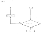
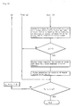
- the distribution of densities and sizes of void defects comprising voids 21 and inner wall membrane 22 in the silicon single crystal 14 was determined by the simulation method whose steps are shown in the flowcharts of Figs. 1 to 4.
- a mesh was applied onto the hot zone of silicon single crystal pulling-up machine 11 for ease of analysis.
- the transverse mesh placed on silicon melt 12 just beneath silicon single crystal 14 had a size of 0.75 mm, while the transverse mesh placed out of the zone of silicon single crystal 14 had a size of 1 to 5 mm.
- the longitudinal mesh placed at the interface between silicon single crystal 14 and melt 12 had a size of 0.25 to 5 mm.
- the eddy current parameter C for the eddy current model equation was set to be 0.45.
- the silicon single crystal 14 was pulled up stepwise by 50 mm from the time to at which the crystal was pulled up till the time t 1 at which the crystal completed cooling process. Under the above-described conditions, the simulation system determined the distribution of temperatures within the silicon single crystal 14 with consideration paid to convection currents in the silicon melt 12.
- the simulation system divided the period from a time to when silicon single crystal 14 was pulled up from silicon melt 12 to a time t 1 when silicon single crystal 14 completed cooling process at specified intervals or ⁇ t seconds (brief time intervals), gathered, for each mesh point of silicon single crystal 14, its coordinates and temperature for each interval ⁇ t, and determined the distribution of internal temperatures of silicon single crystal 14 in terms of the pulled-up length and pulled-up height of silicon single crystal 14. In addition, the system determined the temperature at which void 2firstarted to form, and the distribution of densities and sizes of voids 21.
- the system determined, with the aid of a computer, the distribution of densities and sizes of voids 21 within the silicon single crystal 14 with due consideration paid to the cooling process consisting of slow and rapid cooling phases after the silicon single crystal 14 was separated from silicon melt 12.
- the simulation system it was assumed that oxide membrane 22 grows around a void 21 soon after the formation of the void 21.
- the temperature T p at which oxide membrane 22 starts to form was taken to be equal to the temperature T v at which void 2firstarts to form.
- the term "soon” used here means a "time interval between the formation of void and the next round of computation.”
- the simulation system determined the outer radius R P of inner wall oxide membrane 22 when the temperature was lowered below the membrane formation temperature, and also determined the thickness d of inner wall oxide membrane 22 by subtracting the outer radius R P of inner wall oxide membrane 22 from the radius of void 21.
- the density of inner wall oxide membrane was assumed to be equal to that of voids obtained above.
- the distribution of sizes of void defects comprising voids and inner wall oxide membrane, namely the distribution of inner wall oxide membranes 22 having an outer diameter of R P along a radial direction of the silicon single crystal was determined while the pulling-up speed of the silicon single crystal was varied. The results are indicated by solid lines in Figs.
- LSTD is a sort of aggregate representing air-hole type point defect, and acts as a source of scattering light when exposed to an infrared beam because of its having a refractive index different from that of silicon.
- the distribution of densities and sizes of LSTD observed as above was thought comparable to the distribution of densities and sizes of void defects of Example 1. Since LSTD had a detection limit, it was not possible to detect LSTD having a size smaller than the specific limit.
- a silicon single crystal 14 having a diameter of 6 inch was pulled up from a silicon melt 12 stored in a quartz crucible 13
- the distribution of densities and sizes of void defects comprising voids 21 and inner wall membrane 22 in the silicon single crystal 14 was determined by the simulation method whose steps are shown in the flowcharts of Figs. 7 to 10.
- a mesh was applied onto the hot zone of silicon single crystal pulling-up machine 11 for ease of analysis.
- the transverse mesh placed on silicon melt 12 just beneath silicon single crystal 14 had a size of 0.75 mm, while the transverse mesh placed out of the zone of silicon single crystal 14 had a size of 1 to 5 mm.
- the longitudinal mesh placed at the interface between silicon single crystal 14 and melt 12 had a size of 0.25 to 5 mm.
- the eddy current parameter C for the eddy current model equation was set to be 0.45.
- the silicon single crystal 14 was pulled up stepwise by 50 mm from the time to at which the crystal was pulled up till the time t 1 at which the crystal completed cooling process. Under the above-described conditions, the simulation system determined the distribution of temperatures within the silicon single crystal 14 with consideration paid to convection currents in the silicon melt 12.
- the simulation system divided the period from a time to when silicon single crystal 14 was pulled up from silicon melt 12 to a time t 1 when silicon single crystal 14 completed cooling process at specified intervals or ⁇ t seconds (brief time intervals), gathered, for each mesh point of silicon single crystal 14, its coordinates and temperature for each interval ⁇ t, and determined the distribution of internal temperatures of silicon single crystal 14 in terms of the pulled-up length and pulled-up height of silicon single crystal 14. In addition, the system determined the temperature at which void 2firstarted to form, and the distribution of densities and sizes of voids 21.
- the system determined, with the aid of a computer, the distribution of densities and sizes of voids 21 within the silicon single crystal 14 with due consideration paid to the cooling process consisting of slow and rapid cooling phases after the silicon single crystal 14 was separated from silicon melt 12.
- the simulation system it was assumed that oxide membrane 22 grows around a void 21 soon after the formation of the void 21.
- the temperature T p at which oxide membrane 22 starts to form was taken to be equal to the temperature T v at which void 2 firstarts to form.
- the term "soon” used here means a "time interval between the formation of void and the next round of computation.”
- the simulation system determined the outer radius R P of inner wall oxide membrane 22 when the temperature was lowered below the membrane formation temperature, and also determined the thickness d of inner wall oxide membrane 22 by subtracting the outer radius R P of inner wall oxide membrane 22 from the radius of void 21.
- the density of inner wall oxide membrane was assumed to be equal to that of voids obtained above.
- the system determined, with the aid of the computer, the per-unit-time incidence J c of oxygen precipitation nuclei and their critical radius r cr , based on the distribution of oxygen, of air holes and of temperatures within the silicon single crystal 14.
- the per-unit-time incidence J c of oxygen precipitation nuclei having a radius equal to or above the critical radius r cr exceeds zero, it terminated computation for determining the radius r c of voids and thickness d of inner wall oxide membrane, and determined instead the radius r c of the oxygen precipitation nuclei having a radius equal to or above the critical radius r cr .
- the distributions of sizes and densities of oxygen precipitation nuclei obtained from two different sites (sites A and B of Fig.
- Example 2 A silicon single crystal having the same form with that of Example 1 was pulled up under the same condition, and the resulting silicon single crystal was used as Comparative Example 2.
- the simulation method of the invention for predicting the distribution of densities and sizes of void defects and oxygen precipitation nuclei within a single crystal can be used for improving the quality of silicon single crystal pulled up according to the CZ method.
Landscapes
- Chemical & Material Sciences (AREA)
- Engineering & Computer Science (AREA)
- Crystallography & Structural Chemistry (AREA)
- Materials Engineering (AREA)
- Metallurgy (AREA)
- Organic Chemistry (AREA)
- Crystals, And After-Treatments Of Crystals (AREA)
Applications Claiming Priority (3)
| Application Number | Priority Date | Filing Date | Title |
|---|---|---|---|
| JP2003150262A JP4403722B2 (ja) | 2003-05-28 | 2003-05-28 | シリコン単結晶内ボイド欠陥の密度分布及びサイズ分布のシミュレーション方法 |
| JP2003161493A JP4604462B2 (ja) | 2003-06-06 | 2003-06-06 | 単結晶内酸素析出核の密度分布及びサイズ分布のシミュレーション方法 |
| PCT/JP2004/006822 WO2004106594A1 (ja) | 2003-05-28 | 2004-05-20 | 単結晶内ボイド欠陥と単結晶内酸素析出核の密度分布及びサイズ分布のシミュレーション方法 |
Publications (2)
| Publication Number | Publication Date |
|---|---|
| EP1650331A1 true EP1650331A1 (de) | 2006-04-26 |
| EP1650331A4 EP1650331A4 (de) | 2009-05-13 |
Family
ID=33492426
Family Applications (1)
| Application Number | Title | Priority Date | Filing Date |
|---|---|---|---|
| EP04734077A Ceased EP1650331A4 (de) | 2003-05-28 | 2004-05-20 | Simulationsverfahren bezüglich der dichteverteilung und grössenverteilung von leerstellendefekt in einkristall und sauerstoffausscheidungskeim in einkristall |
Country Status (5)
| Country | Link |
|---|---|
| US (1) | US7282094B2 (de) |
| EP (1) | EP1650331A4 (de) |
| KR (1) | KR100719207B1 (de) |
| DE (1) | DE04734077T1 (de) |
| WO (1) | WO2004106594A1 (de) |
Cited By (1)
| Publication number | Priority date | Publication date | Assignee | Title |
|---|---|---|---|---|
| DE102012112836A1 (de) | 2012-12-21 | 2014-06-26 | Technische Universität Dresden | Verfahren zur rückführenden Simulation von Halbleiterstrukturen |
Families Citing this family (6)
| Publication number | Priority date | Publication date | Assignee | Title |
|---|---|---|---|---|
| KR102138121B1 (ko) * | 2013-11-07 | 2020-07-27 | 에스케이실트론 주식회사 | 실리콘 단결정 잉곳 제조 장치 및 제조 방법 |
| CN107747122B (zh) * | 2017-09-11 | 2020-03-31 | 西安理工大学 | 一种直拉硅单晶生长工艺优化固液界面氧分布调节方法 |
| US11047066B2 (en) | 2018-06-27 | 2021-06-29 | Globalwafers Co., Ltd. | Growth of plural sample rods to determine impurity build-up during production of single crystal silicon ingots |
| US10954606B2 (en) * | 2018-06-27 | 2021-03-23 | Globalwafers Co., Ltd. | Methods for modeling the impurity concentration of a single crystal silicon ingot |
| WO2022172367A1 (ja) * | 2021-02-10 | 2022-08-18 | グローバルウェーハズ・ジャパン株式会社 | エピタキシャルシリコンウェーハにおける欠陥の発生予測方法およびエピタキシャルシリコンウェーハの製造方法 |
| CN114464264A (zh) * | 2021-12-31 | 2022-05-10 | 深圳晶泰科技有限公司 | 基于分子动力学的晶体熔点的计算方法、装置及存储介质 |
Family Cites Families (13)
| Publication number | Priority date | Publication date | Assignee | Title |
|---|---|---|---|---|
| US5154795A (en) * | 1989-06-12 | 1992-10-13 | Mitsubishi Kasei Polytec Company | System for setting analysis condition for a thermal analysis of a fluid inside an apparatus |
| JPH0777996B2 (ja) * | 1990-10-12 | 1995-08-23 | 信越半導体株式会社 | コーン部育成制御方法及び装置 |
| JP2807609B2 (ja) * | 1993-01-28 | 1998-10-08 | 三菱マテリアルシリコン株式会社 | 単結晶の引上装置 |
| US5779791A (en) * | 1996-08-08 | 1998-07-14 | Memc Electronic Materials, Inc. | Process for controlling thermal history of Czochralski-grown silicon |
| TW541365B (en) * | 1996-08-30 | 2003-07-11 | Sumitomo Sitix Corp | Single crystal pulling method and single crystal pulling device |
| TW574445B (en) * | 1997-03-19 | 2004-02-01 | Komatsu Denshi Kinzoku Kk | Defect-control method of silicon single-crystal |
| JPH11190662A (ja) * | 1997-12-26 | 1999-07-13 | Sumitomo Sitix Corp | 単結晶引上炉内融液の表面温度測定方法及び該方法に用いる装置 |
| US6171391B1 (en) * | 1998-10-14 | 2001-01-09 | Memc Electronic Materials, Inc. | Method and system for controlling growth of a silicon crystal |
| JP3846155B2 (ja) * | 2000-04-26 | 2006-11-15 | 株式会社Sumco | 単結晶及び融液の固液界面形状のシミュレーション方法 |
| TW498402B (en) * | 2000-04-26 | 2002-08-11 | Mitsubishi Material Silicon | Method for simulating the shape of the solid-liquid interface between a single crystal and a molten liquid, and the distribution of point defect of a single crystal |
| JP4106880B2 (ja) | 2001-07-27 | 2008-06-25 | 株式会社Sumco | 単結晶内欠陥の密度分布及びサイズ分布のシミュレーション方法 |
| AU2003290909A1 (en) * | 2002-07-05 | 2004-03-11 | Sumitomo Mitsubishi Silicon Corporation | Method of producing silicon monocrystal |
| US7074271B2 (en) * | 2004-02-23 | 2006-07-11 | Sumitomo Mitsubishi Silicon Corporation | Method of identifying defect distribution in silicon single crystal ingot |
-
2003
- 2003-05-30 US US10/558,790 patent/US7282094B2/en not_active Expired - Lifetime
-
2004
- 2004-05-20 EP EP04734077A patent/EP1650331A4/de not_active Ceased
- 2004-05-20 DE DE04734077T patent/DE04734077T1/de active Pending
- 2004-05-20 KR KR1020057022730A patent/KR100719207B1/ko not_active Expired - Lifetime
- 2004-05-20 WO PCT/JP2004/006822 patent/WO2004106594A1/ja not_active Ceased
Non-Patent Citations (2)
| Title |
|---|
| No Search * |
| See also references of WO2004106594A1 * |
Cited By (2)
| Publication number | Priority date | Publication date | Assignee | Title |
|---|---|---|---|---|
| DE102012112836A1 (de) | 2012-12-21 | 2014-06-26 | Technische Universität Dresden | Verfahren zur rückführenden Simulation von Halbleiterstrukturen |
| DE102012112836B4 (de) * | 2012-12-21 | 2017-11-02 | Technische Universität Dresden | Verfahren zur rückführenden Simulation von Halbleiterstrukturen |
Also Published As
| Publication number | Publication date |
|---|---|
| KR20060015319A (ko) | 2006-02-16 |
| EP1650331A4 (de) | 2009-05-13 |
| US20060243192A1 (en) | 2006-11-02 |
| DE04734077T1 (de) | 2006-10-12 |
| WO2004106594A1 (ja) | 2004-12-09 |
| KR100719207B1 (ko) | 2007-05-16 |
| US7282094B2 (en) | 2007-10-16 |
Similar Documents
| Publication | Publication Date | Title |
|---|---|---|
| Riley et al. | Instability of thermocapillary–buoyancy convection in shallow layers. Part 1. Characterization of steady and oscillatory instabilities | |
| US5485803A (en) | Method of predicting crystal quality of semiconductor single crystal and apparatus thereof | |
| EP1541721B1 (de) | Verfahren zur herstellung von silicium-einkristall | |
| WO2001071069A1 (en) | Method for producing silicon single crystal having no flaw | |
| Virzi | Computer modelling of heat transfer in Czochralski silicon crystal growth | |
| EP1650331A1 (de) | Simulationsverfahren bezüglich der dichteverteilung und grössenverteilung von leerstellendefekt in einkristall und sauerstoffausscheidungskeim in einkristall | |
| Popescu et al. | Effect of crucible rotation on the temperature and oxygen distributions in Czochralski grown silicon for photovoltaic applications | |
| US6451107B2 (en) | Method for simulating the shape of the solid-liquid interface between a single crystal and a molten liquid, and the distribution of point defects of the single crystal | |
| Van den Bogaert et al. | Dynamic global simulation of the Czochralski process II. Analysis of the growth of a germanium crystal | |
| Chen et al. | Measurement of the float-zone interface shape for lithium niobate | |
| Kranert et al. | Facet growth and geometry of the growth ridge during dynamic Czochralski processes | |
| JP4106880B2 (ja) | 単結晶内欠陥の密度分布及びサイズ分布のシミュレーション方法 | |
| JP4403722B2 (ja) | シリコン単結晶内ボイド欠陥の密度分布及びサイズ分布のシミュレーション方法 | |
| KR100665683B1 (ko) | 실리콘 단결정 제조방법 | |
| JP2004363412A (ja) | 単結晶内酸素析出核の密度分布及びサイズ分布のシミュレーション方法 | |
| Masi et al. | Sensitivity analysis on indium phosphide liquid encapsulated czochralski growth | |
| Kitamura et al. | Radial distribution of temperature gradients in growing CZ-Si crystals and its application to the prediction of microdefect distribution | |
| JP4449347B2 (ja) | シミュレーションによるosfリングの分布予測方法 | |
| JP4096499B2 (ja) | 単結晶の点欠陥分布のシミュレーション方法 | |
| JP4192704B2 (ja) | 単結晶の無欠陥領域を最大化するシミュレーション方法 | |
| JP3846155B2 (ja) | 単結晶及び融液の固液界面形状のシミュレーション方法 | |
| Lereah et al. | High resolution electron microscopy of crystalline–amorphous interface: An indication to Eden aggregate | |
| Kawamata et al. | Migration rate of lenticular voids in UO2 under the influence of temperature gradient | |
| US5948159A (en) | Method of controlling defects of a silicon single crystal | |
| Wei et al. | Effect of dynamic perturbation and contact condition on edge-defined fiber growth characteristics |
Legal Events
| Date | Code | Title | Description |
|---|---|---|---|
| PUAI | Public reference made under article 153(3) epc to a published international application that has entered the european phase |
Free format text: ORIGINAL CODE: 0009012 |
|
| 17P | Request for examination filed |
Effective date: 20051228 |
|
| AK | Designated contracting states |
Kind code of ref document: A1 Designated state(s): DE |
|
| DAX | Request for extension of the european patent (deleted) | ||
| RBV | Designated contracting states (corrected) |
Designated state(s): DE |
|
| DET | De: translation of patent claims | ||
| A4 | Supplementary search report drawn up and despatched |
Effective date: 20090416 |
|
| 17Q | First examination report despatched |
Effective date: 20130218 |
|
| REG | Reference to a national code |
Ref country code: DE Ref legal event code: R003 |
|
| STAA | Information on the status of an ep patent application or granted ep patent |
Free format text: STATUS: THE APPLICATION HAS BEEN REFUSED |
|
| 18R | Application refused |
Effective date: 20170623 |