EP1649476B1 - Hochfrequenz-doppelpol-einzelbetätigungs-schalter - Google Patents
Hochfrequenz-doppelpol-einzelbetätigungs-schalter Download PDFInfo
- Publication number
- EP1649476B1 EP1649476B1 EP04777018.5A EP04777018A EP1649476B1 EP 1649476 B1 EP1649476 B1 EP 1649476B1 EP 04777018 A EP04777018 A EP 04777018A EP 1649476 B1 EP1649476 B1 EP 1649476B1
- Authority
- EP
- European Patent Office
- Prior art keywords
- transistors
- circuit portion
- coupled
- input port
- isolation
- Prior art date
- Legal status (The legal status is an assumption and is not a legal conclusion. Google has not performed a legal analysis and makes no representation as to the accuracy of the status listed.)
- Expired - Lifetime
Links
- 238000002955 isolation Methods 0.000 claims description 18
- 230000008878 coupling Effects 0.000 claims description 3
- 238000010168 coupling process Methods 0.000 claims description 3
- 238000005859 coupling reaction Methods 0.000 claims description 3
- 230000015556 catabolic process Effects 0.000 description 2
- 230000005540 biological transmission Effects 0.000 description 1
- 239000003990 capacitor Substances 0.000 description 1
- 238000007796 conventional method Methods 0.000 description 1
- 238000010586 diagram Methods 0.000 description 1
- 238000012986 modification Methods 0.000 description 1
- 230000004048 modification Effects 0.000 description 1
Images


Classifications
-
- H—ELECTRICITY
- H01—ELECTRIC ELEMENTS
- H01H—ELECTRIC SWITCHES; RELAYS; SELECTORS; EMERGENCY PROTECTIVE DEVICES
- H01H9/00—Details of switching devices, not covered by groups H01H1/00 - H01H7/00
- H01H9/54—Circuit arrangements not adapted to a particular application of the switching device and for which no provision exists elsewhere
-
- H—ELECTRICITY
- H01—ELECTRIC ELEMENTS
- H01P—WAVEGUIDES; RESONATORS, LINES, OR OTHER DEVICES OF THE WAVEGUIDE TYPE
- H01P1/00—Auxiliary devices
- H01P1/10—Auxiliary devices for switching or interrupting
-
- H—ELECTRICITY
- H01—ELECTRIC ELEMENTS
- H01P—WAVEGUIDES; RESONATORS, LINES, OR OTHER DEVICES OF THE WAVEGUIDE TYPE
- H01P1/00—Auxiliary devices
- H01P1/10—Auxiliary devices for switching or interrupting
- H01P1/15—Auxiliary devices for switching or interrupting by semiconductor devices
Definitions
- This present invention relates to radiofrequency switches, and in particular, to microwave/millimeter wave switches.
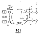
- FIG. 1 shows a monopulse-type radar receiver 10, which is one example of an application which requires a DPST switch.
- the radar receiver 10 includes first and second reception antennae 20, 30 which are coupled to the two inputs of the DPST switch 50 through low-noise amplifiers (LNAs) 40, 45.
- LNAs low-noise amplifiers
- the DPST switch 50 is used to select between one of the two reception antennae 20, 30, and thus select one of two received signals.
- the output of the DPST switch 50 is coupled to mixers 60, 65 which separate the received signal into in-phase (I) and quadrature phase (Q) components.
- DPST switches operating at microwave and millimeter wave frequencies include complex networks based upon diodes and transmission lines than can be large and expensive.
- US 2002/0113640 discloses a multiplexer circuit for performing time-division multiplexing.
- the multiplexer circuit has two or more select lines for selecting alternate ones of input signal pairs during operation, and two or more resistive loads and associated electronic gates.
- a receiver apparatus comprising at least one antenna and at least one switch according to any one of the appended claims.
- Embodiments of the present invention comprises a Double Pole Single Throw (DPST) switch which may be fabricated as an integrated circuit (IC).
- DPST Double Pole Single Throw
- IC integrated circuit
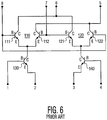
- FIG. 6 shows an exemplary Gilbert Cell 100 which includes a first differential amplifier pair 110 (including transistors 111, 112), and a second differential amplifier pair 120 (including transistors 121, 122).
- the collectors of transistors 111 and 121 are coupled to each other and to pin "5" of the Gilbert Cell 100.
- the collectors of transistors 112 and 122 are coupled to each other and to pin "6" of the Gilbert Cell 100.
- the bases of transistors 111 and 122 are coupled to each other and to pin "8" of the Gilbert Cell 100, and the bases of transistors 112 and 121 are coupled to each other and to pin “7" of the Gilbert Cell.
- the emitters of the transistors 111, 112 of the first differential amplifier pair 110 are coupled to the collector of a first bias transistor 130, and the emitters of the transistors 121, 122 of the second differential amplifier pair 120 are coupled to the collector of a second bias transistor 140.
- a differential AC bias voltage applied to the bases of the first and second bias transistors 130,140 controls the amplitude of an input radio frequency (RF) signal applied across pins "6" and "7” of the Gilbert Cell.
- RF radio frequency
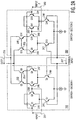
- FIG. 2 (a) shows a DPST switch circuit 200 according to a first exemplary embodiment of the present invention.
- the DPST switch circuit 200 includes a first input port 201, a second input port 202, and a first output port 203.
- the switch circuit 200 also includes a first switch section 205 corresponding to the first input port 201, and a second switch section 206 corresponding to the second input port 202.
- a control input port 207 provides a voltage signal controlling which of the switch sections 205, 206 are active (i.e., transmitting their signal to the output port 203).
- the first switch section 205 includes transistors 240, 241', 245, 247, 250, 252, 254, and 256
- the second switch section 206 includes transistors 241, 240', 246, 248, 251, 253, 255, and 257.
- a control voltage is applied to control input port 207 such that the voltage applied to the base of either transistors 240 and 240' (Q8, Q16) or transistors 241 and 241' (Q7, Q15) is higher than the voltage applied to the other set of transistors by the thermal breakdown voltage of the transistors (e.g., 0.7 Volts (V)).
- transistors 240, 240' are biased 'ON' and the second input port 202 'sees' a high input impedance, and thus the signal at the first input port 201 is transmitted to the output port 203.
- transistors 241, 241' are biased 'ON' and the first input port 201 'sees' a high input impedance, and thus the signal at the second input port 202 is transmitted to the output port 203.
- first input port 201 is coupled to output port 203 (e.g., where transistors 240 and 240' are biased 'ON')
- transistors 251 and 257 are also biased 'ON'
- transistors 246, 248, 253 and 255 are biased 'OFF' so that the second section 206 doesn't load the output of the first switch section 205 at all, and all of the signal transmitted from the first input port 201 will appear at the output port 203.
- transistors 250 and 256 are also biased 'ON' and transistors 245, 247, 252 and 254 (Q3, Q4, Q5, Q6) are biased 'OFF" so that the first section 205 doesn't load the output of the second switch section 206 at all, and all of the signal transmitted from the second input port 202 will appear at the output port 203. Further details of the operation of the switch circuit 200 are discussed below with reference to Figure 2(b) .
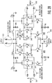
- Figure 2(b) shows the DPST switch circuit 200 according to a first exemplary embodiment of the present invention in greater detail. Many of the elements shown in Figure 2(b) were also shown in Figure 2(a) , and like reference numerals indicate like elements.
- the DPST switch circuit 200 includes a first input port 201, a second input port 202, and a first output port 203.
- a supply voltage V dc is provided to a network of transistor switches 208 (comprised of first section 205 and second section 206) coupled between the inputs 201, 202 and the output 203.
- Inductors 210, 211 provide isolation between the DC supply voltage V dc and the AC voltage at the input ports 201, 202 and output port 203.
- capacitors 215, 216 isolate DC voltages from the output port 203.
- the network includes bias transistors 240, 240', 241, and 241' (corresponding to bias transistors 130, 140 of the Gilbert Cell shown in Figure 14), interior transistors 245, 246 (corresponding to transistors 112, 121 of the Gilbert Cell shown in Figure 14), and exterior transistors 247, 248 (corresponding to transistors 111, 122 of the Gilbert Cell shown in Figure 14).
- bias transistors 240, 240', 241, and 241' corresponding to bias transistors 130, 140 of the Gilbert Cell shown in Figure 14
- interior transistors 245, 246 corresponding to transistors 112, 121 of the Gilbert Cell shown in Figure 14
- exterior transistors 247, 248 corresponding to transistors 111, 122 of the Gilbert Cell shown in Figure 14
- additional transistors 250-257 are provided around the 'modified' Gilbert Cell.
- FIG. 2(b) For ease of illustration, not all of the biasing circuitry for each of the transistors 240, 240', 241, 241', 245-248 and 250-257 is shown in Figure 2(b)
- Bias transistors 240 and 241', and 241 and 240' have their emitters coupled together and to a current source I dc .
- the bases of the bias transistors 240, 240' are fed by a first voltage source V dc1 and the bases of bias transistors 241, 241' are fed by a second voltage source V dc2 .
- transistor pairs 250/256, 245/247, 246/248, and 251/257 of the switch circuit 200 are all coupled in a 'cascode' configuration (i.e., emitter coupled).
- This cascode coupling of the transistors presents a high input impedance to each of the input ports 201 and 202.
- input port 201 presents a high input impedance
- input port 202 presents a high input impedance
- input port 201 presents a high input impedance.
- the high input impedance prevents either of the unwanted ports (e.g., either input port 201 or 202) from loading the desired signal path.
- the cascode configuration of the transistor pairs 250/256, 245/247, 246/248, and 251/257 has little or no effect on the isolation between wanted and unwanted signals. It does, however, ensure that the wanted signal is directed to the output port 203 instead of being lost traveling to the other input port.
- This high input impedance prevents extraneous signals from the unselected input port from being applied to the switch circuit 200.
- Each of the two input ports 201, 202 is coupled to a separate portion of the network of transistors 208.
- input port 201 is coupled to a first portion 205 including transistors 240, 241', 245, 247, 250, 252, 254 and 256
- input port 202 is coupled to a second portion 206 including transistors 240', 241, 246, 248, 251, 253, 255 and 257.
- Each of the these first and second portions 205, 206 further include both a 'transmit' channel and an 'isolation' channel.
- the 'transmit' channel for the first portion 205 (corresponding to input port 201) comprises transistors 245, 247, 252 and 254, and the 'isolation' channel comprises transistors 250 and 256.
- the 'transmit' channel for the second portion 206 comprises transistors 246, 248, 253 and 255
- the 'isolation' channel comprises transistors 251 and 257.
- signals are applied to input ports 201 and 202, and either the input signal at port 201 or the input signal at port 202 is transmitted to the output port 203 at any given instant.
- the selection of which input port (e.g., 201 or 202) is applied to the output port 203 is accomplished by applying different voltages to the bases of bias transistors 240, 240', 241, and 241'.
- voltage sources V dc1 and V dc2 directly control the voltage applied to the respective bases of the bias transistor 240, 240', 241, and 241'.
- bias transistors 240 and 240' have a greater voltage applied thereto than bias transistors 241 and 241' (by at least approximately 0.7 volts, which is the thermal breakdown voltage of the bias transistors)
- input port 201 will be coupled to output port 203.
- bias transistors 241 and 241' have a greater voltage applied thereto than bias transistors 240 and 240' (by at least approximately 0.7 volts)
- input port 202 will be coupled to output port 203.
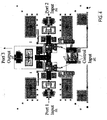
- Figure 3 shows the switch circuit 200 of Figure 2 implemented monolithically.
- Figure 4 is an enlarged view of a portion of the monolithically-implemented switch circuit 200 showing the input ports 201, 202, and the output port 203 in greater detail.
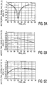
- Figures 5(a)-5(i) are graphs showing a frequency in GigaHertz (GHz) versus decibel (dB) response for the switch circuit 200 of Figure 2 .
- Figures 5(a) , (e) and (i) show input impedance matching curves for input ports 201 (Port 1), 202 (Port 2) and output port 203 (Port 3), respectively.
- the remaining figures show isolation curves for the switch circuit 200 as between different ports (e.g., Figure 5(b) shows an isolation curve between one of the input ports (Port 2) and another of the input ports (Port 1).
- the isolation between the ports 201-203 of the switch circuit 200 is relatively uniform across the operational frequency range.
- the switch circuit 200 is always matched (i.e., the return loss of each port 201-203 stays constant irrespective of the switch's state).
Landscapes
- Electronic Switches (AREA)
- Waveguide Switches, Polarizers, And Phase Shifters (AREA)
Claims (4)
- Empfangsvorrichtung, die wenigstens eine Antenne und wenigstens einen mit der Antenne gekoppelten Schalter (200) umfasst, wobei der genannte Schalter Folgendes umfasst:einen ersten Schaltkreisabschnitt (205) entsprechend einem ersten Eingangsport (201),einen zweiten Schaltkreisabschnitt (206) entsprechend einem zweiten Eingangsport (202), undeinen Ausgangsport (203),wobei der erste Schaltkreisabschnitt (205) einen Isolationskanal mit wenigstens einem ersten Differentialverstärkerpaar von zwei Transistoren (256, 250) umfasst, wobei der genannte Isolationskanal Isolation zwischen dem ersten Eingangsport (201) und dem Ausgangsport (203) bereitstellt, einen Sendekanal mit wenigstens einem zweiten Differentialverstärkerpaar von zwei Transistoren (245, 247), wobei der genannte Sendekanal Kopplung zwischen dem ersten Eingangsport (201) und dem Ausgangsport (203) bereitstellt, und wenigstens einen dritten Transistor (241', 240) zum Erzeugen einer Steuervorspannung zum Wählen des Isolationskanals oder des Sendekanals des ersten Schaltkreisabschnitts (205), wobei der Isolations- und der Sendekanal des ersten Schaltkreisabschnitts (205) eine konstante Rückflussdämpfung am ersten Eingangsport (201) unabhängig davon bereitstellen, welcher Kanal des ersten Schaltkreisabschnitts (205) gewählt ist,wobei der zweite Schaltkreisabschnitt (206) einen Isolationskanal mit wenigstens einem ersten Differentialverstärkerpaar von zwei Transistoren (251, 257) beinhaltet, wobei der genannte Isolationskanal Isolation zwischen dem zweiten Eingangsport (202) und dem Ausgangsport (203) bereitstellt, einen Sendekanal mit wenigstens einem zweiten Differentialverstärkerpaar von zwei Transistoren (248, 246), wobei der genannte Sendekanal Kopplung zwischen dem zweiten Eingangsport (202) und dem Ausgangsport (203) bereitstellt, und wenigstens einen dritten Transistor (240', 241) zum Bereitstellen einer Steuervorspannung zum Wählen entweder des Isolationskanals oder des Sendekanals des zweiten Schaltkreisabschnitts, wobei der Isolations- und der Sendekanal des zweiten Schaltkreisabschnitts (206) eine konstante Rückflussdämpfung am zweiten Eingangsport (202) unabhängig davon bereitstellen, welcher Kanal des zweiten Schaltkreisabschnitts (206) gewählt ist,wobei der wenigstens eine dritte Transistor (240, 240', 241, 241') von jedem aus erstem und zweitem Schaltkreisabschnitt die Steuervorspannung zum Wählen bereitstellt, welcher aus erstem und zweiten Eingangsport (201, 202) mit dem Ausgangsport (203) gekoppelt wird.
- Schaltkreis (200) nach Anspruch 1, wobei der Kreis als integrierte Schaltung ausgebildet ist.
- Schaltkreis (200) nach Anspruch 1, wobei wenigstens ein dritter Transistor zwei Transistoren umfasst.
- Schaltkreis (200) nach Anspruch 1, wobei:die jeweiligen Emitter der beiden Transistoren (256, 250) des ersten Differentialpaars des ersten Schaltkreisabschnitts miteinander gekoppelt sind und zusätzlich mit einem Kollektor des wenigstens einen dritten Transistors (241') des ersten Schaltkreisabschnitts gekoppelt sind,die jeweiligen Emitter der beiden Transistoren (245, 247) des zweiten Differentialpaars des ersten Schaltkreisabschnitts miteinander gekoppelt sind und zusätzlich mit einem Kollektor des wenigstens einen dritten Transistors (240) des ersten Schaltkreisabschnitts gekoppelt sind,die jeweiligen Emitter der beiden Transistoren (251, 257) des ersten Differentialpaars des zweiten Schaltkreisabschnitts miteinander gekoppelt sind und zusätzlich mit einem Kollektor des wenigstens einen dritten Transistors (240') des zweiten Schaltkreisabschnitts gekoppelt sind,die jeweiligen Emitter der beiden Transistoren (248, 246) des zweiten Differentialpaars des zweiten Schaltkreisabschnitts miteinander gekoppelt sind und zusätzlich mit einem Kollektor des wenigstens einen dritten Transistors (241) des zweiten Schaltkreisabschnitts gekoppelt sind.
Applications Claiming Priority (2)
| Application Number | Priority Date | Filing Date | Title |
|---|---|---|---|
| US10/621,147 US7547993B2 (en) | 2003-07-16 | 2003-07-16 | Radiofrequency double pole single throw switch |
| PCT/US2004/020252 WO2005010906A2 (en) | 2003-07-16 | 2004-06-23 | Radiofrequency double pole single throw switch |
Publications (2)
| Publication Number | Publication Date |
|---|---|
| EP1649476A2 EP1649476A2 (de) | 2006-04-26 |
| EP1649476B1 true EP1649476B1 (de) | 2019-03-27 |
Family
ID=34062928
Family Applications (1)
| Application Number | Title | Priority Date | Filing Date |
|---|---|---|---|
| EP04777018.5A Expired - Lifetime EP1649476B1 (de) | 2003-07-16 | 2004-06-23 | Hochfrequenz-doppelpol-einzelbetätigungs-schalter |
Country Status (6)
| Country | Link |
|---|---|
| US (1) | US7547993B2 (de) |
| EP (1) | EP1649476B1 (de) |
| JP (1) | JP2007531348A (de) |
| KR (1) | KR101093882B1 (de) |
| CN (1) | CN1853346A (de) |
| WO (1) | WO2005010906A2 (de) |
Families Citing this family (8)
| Publication number | Priority date | Publication date | Assignee | Title |
|---|---|---|---|---|
| JP2007274428A (ja) * | 2006-03-31 | 2007-10-18 | Thine Electronics Inc | アナログマルチプレクサ |
| US7808342B2 (en) * | 2006-10-02 | 2010-10-05 | Skyworks Solutions, Inc. | Harmonic phase tuning filter for RF switches |
| US7839234B2 (en) * | 2006-10-02 | 2010-11-23 | Skyworks Solutions, Inc. | Switching module with harmonic phase tuning filter |
| US7646260B2 (en) * | 2007-07-13 | 2010-01-12 | Skyworks Solutions, Inc. | Switching device with selectable phase shifting modes for reduced intermodulation distortion |
| US7817966B2 (en) * | 2007-07-13 | 2010-10-19 | Skyworks Solutions, Inc. | Switching device with reduced intermodulation distortion |
| CN101673861B (zh) * | 2009-10-12 | 2013-05-01 | 京信通信系统(中国)有限公司 | 一种单刀双掷射频开关装置及其实现方法 |
| US10193507B1 (en) * | 2017-07-31 | 2019-01-29 | Analog Devices Global | Current switching circuit |
| US11105891B2 (en) * | 2018-12-13 | 2021-08-31 | Semiconductor Components Industries, Llc | Multi-input downconversion mixer |
Citations (1)
| Publication number | Priority date | Publication date | Assignee | Title |
|---|---|---|---|---|
| US20020113640A1 (en) * | 2001-02-21 | 2002-08-22 | Jenkins Julian L. | Method for achieving low feed-through and consistent transition delay in a multiplexor circuit |
Family Cites Families (36)
| Publication number | Priority date | Publication date | Assignee | Title |
|---|---|---|---|---|
| US3798376A (en) * | 1969-12-29 | 1974-03-19 | Rca Corp | Multiplex decoding system |
| JPS58181310A (ja) | 1982-04-15 | 1983-10-24 | Mitsubishi Electric Corp | 電圧利得制御増幅装置 |
| US4460873A (en) * | 1982-11-19 | 1984-07-17 | Control Data Corporation | Active differential output direct current offset voltage compensation circuit for a differential amplifier |
| JP2621311B2 (ja) * | 1988-03-10 | 1997-06-18 | 日本電気株式会社 | ラッチ回路付きコンパレータ |
| JPH04150310A (ja) * | 1990-10-11 | 1992-05-22 | Matsushita Electric Ind Co Ltd | アナログスイッチ回路 |
| JP2875922B2 (ja) * | 1992-03-05 | 1999-03-31 | 三菱電機株式会社 | A/d変換器 |
| DE4235909C2 (de) * | 1992-10-23 | 2003-01-02 | Atmel Germany Gmbh | Mono/Stereo-Umschalter |
| US5487048A (en) * | 1993-03-31 | 1996-01-23 | Sgs-Thomson Microelectronics, Inc. | Multiplexing sense amplifier |
| JP2713167B2 (ja) * | 1994-06-14 | 1998-02-16 | 日本電気株式会社 | 比較器 |
| EP0691734B1 (de) * | 1994-07-08 | 2001-08-22 | Infineon Technologies AG | Verstärkeranordnung für Hochfrequenzsignale |
| US5448772A (en) * | 1994-08-29 | 1995-09-05 | Motorola, Inc. | Stacked double balanced mixer circuit |
| US5901350A (en) * | 1996-09-30 | 1999-05-04 | Fairchild Semiconductor Corporation | Low distortion large swing frequency down coverter filter amplifier circuit |
| JPH10173547A (ja) * | 1996-12-11 | 1998-06-26 | Matsushita Electric Ind Co Ltd | 送信出力検出回路 |
| DE19725286A1 (de) * | 1997-06-14 | 1998-12-17 | Philips Patentverwaltung | Schaltungsanordnung mit einer Differenzverstärkerstufe |
| JP3506587B2 (ja) * | 1997-08-19 | 2004-03-15 | アルプス電気株式会社 | 二重平衡変調器及び四相位相変調器並びにデジタル通信機 |
| US6054889A (en) * | 1997-11-11 | 2000-04-25 | Trw Inc. | Mixer with improved linear range |
| US6137852A (en) * | 1997-12-23 | 2000-10-24 | Motorola, Inc | Phase detector circuit and method of phase detecting |
| US6188339B1 (en) * | 1998-01-23 | 2001-02-13 | Fuji Photo Film Co., Ltd. | Differential multiplexer and differential logic circuit |
| US6393260B1 (en) * | 1998-04-17 | 2002-05-21 | Nokia Mobile Phones Limited | Method for attenuating spurious signals and receiver |
| US6073002A (en) * | 1998-05-04 | 2000-06-06 | Motorola | Mixer circuit and communication device using the same |
| DE69822836T2 (de) * | 1998-10-30 | 2005-03-24 | Stmicroelectronics S.R.L., Agrate Brianza | I-Q Mischer mit niedrigem Rauschen |
| JP2000174576A (ja) * | 1998-12-08 | 2000-06-23 | Fujitsu Ltd | 可変利得増幅器 |
| US6573760B1 (en) * | 1998-12-28 | 2003-06-03 | Agere Systems Inc. | Receiver for common mode data signals carried on a differential interface |
| US6157257A (en) * | 1999-06-30 | 2000-12-05 | Conexant Systems, Inc. | Low power folding amplifier |
| JP2001274707A (ja) * | 2000-03-27 | 2001-10-05 | Clarion Co Ltd | 受信装置 |
| WO2002045253A1 (en) * | 2000-12-01 | 2002-06-06 | Mitsubishi Denki Kabushiki Kaisha | High-frequency amplifier |
| JP2002223126A (ja) * | 2001-01-29 | 2002-08-09 | Fujitsu Ltd | 周波数逓倍装置 |
| US6642878B2 (en) * | 2001-06-06 | 2003-11-04 | Furaxa, Inc. | Methods and apparatuses for multiple sampling and multiple pulse generation |
| US6680625B1 (en) * | 2002-01-31 | 2004-01-20 | Lattice Semiconductor Corp. | Symmetrical CML logic gate system |
| US6518842B1 (en) * | 2002-06-07 | 2003-02-11 | Analog Devices, Inc. | Bipolar rail-to-rail input stage with selectable transition threshold |
| US6819201B2 (en) * | 2002-07-19 | 2004-11-16 | M/A-Com | Balanced high isolation fast state transitioning switch apparatus |
| US7088170B2 (en) * | 2003-06-30 | 2006-08-08 | International Business Machines Corporation | Multiplexer and demultiplexer |
| US6987419B2 (en) * | 2003-07-07 | 2006-01-17 | M/A-Com, Inc. | Absorptive microwave single pole single throw switch |
| US6940352B2 (en) * | 2003-11-26 | 2005-09-06 | Scintera Networks, Inc. | Analog signal interpolation |
| US7123074B2 (en) * | 2004-02-24 | 2006-10-17 | Micrel, Inc. | Method and system for multichannel-isolation-technique multiplexer |
| US7386290B2 (en) * | 2004-07-30 | 2008-06-10 | Broadcom Corporation | RX dual-band mixer |
-
2003
- 2003-07-16 US US10/621,147 patent/US7547993B2/en not_active Expired - Fee Related
-
2004
- 2004-06-23 WO PCT/US2004/020252 patent/WO2005010906A2/en not_active Ceased
- 2004-06-23 EP EP04777018.5A patent/EP1649476B1/de not_active Expired - Lifetime
- 2004-06-23 CN CNA200480026431XA patent/CN1853346A/zh active Pending
- 2004-06-23 JP JP2006520187A patent/JP2007531348A/ja active Pending
- 2004-06-23 KR KR1020067001017A patent/KR101093882B1/ko not_active Expired - Fee Related
Patent Citations (1)
| Publication number | Priority date | Publication date | Assignee | Title |
|---|---|---|---|---|
| US20020113640A1 (en) * | 2001-02-21 | 2002-08-22 | Jenkins Julian L. | Method for achieving low feed-through and consistent transition delay in a multiplexor circuit |
Also Published As
| Publication number | Publication date |
|---|---|
| WO2005010906A8 (en) | 2005-10-06 |
| WO2005010906A2 (en) | 2005-02-03 |
| CN1853346A (zh) | 2006-10-25 |
| KR101093882B1 (ko) | 2011-12-13 |
| EP1649476A2 (de) | 2006-04-26 |
| US20050012400A1 (en) | 2005-01-20 |
| JP2007531348A (ja) | 2007-11-01 |
| US7547993B2 (en) | 2009-06-16 |
| KR20060033801A (ko) | 2006-04-19 |
Similar Documents
| Publication | Publication Date | Title |
|---|---|---|
| US10879623B2 (en) | Method to improve power amplifier output return loss and back-off performance with RC feedback network | |
| US5760645A (en) | Demodulator stage for direct demodulation of a phase quadrature modulated signal and receiver including a demodulator stage of this kind | |
| US6259301B1 (en) | Method and apparatus for selecting from multiple mixers | |
| US8482364B2 (en) | Differential cross-coupled power combiner or divider | |
| KR100189309B1 (ko) | 모놀리식 다중 기능 밸런스 스위치 및 위상 시프터 | |
| CN110784179B (zh) | 一种双平衡fet混频器 | |
| US7843282B2 (en) | Phase shifter with flexible control voltage | |
| US8467739B2 (en) | Monolithic integrated transceiver | |
| US6242990B1 (en) | Quadrature phase shift keyed/bi-phase shift keyed modulator | |
| US6950634B2 (en) | Transceiver circuit arrangement and method | |
| US6459885B1 (en) | Radio transceiver switching circuit | |
| US6950631B2 (en) | Active receiving array antenna | |
| EP1649476B1 (de) | Hochfrequenz-doppelpol-einzelbetätigungs-schalter | |
| US12199578B2 (en) | Amplifiers suitable for mm-wave signal splitting and combining | |
| US7817968B2 (en) | Transmitter and receiver circuit | |
| US5323064A (en) | Radio frequency signal frequency converter | |
| EP0714177A2 (de) | Funkgerät für Zeitmultiplex | |
| US7511592B2 (en) | Switch circuit and integrated circuit | |
| US20080258821A1 (en) | Cmos triple-band rf vga and power amplifier in linear transmitter | |
| US5748049A (en) | Multi-frequency local oscillators | |
| WO2001052426A2 (en) | Improved mmic transceiver | |
| JPH02238710A (ja) | スイッチ回路 |
Legal Events
| Date | Code | Title | Description |
|---|---|---|---|
| PUAI | Public reference made under article 153(3) epc to a published international application that has entered the european phase |
Free format text: ORIGINAL CODE: 0009012 |
|
| 17P | Request for examination filed |
Effective date: 20060208 |
|
| AK | Designated contracting states |
Kind code of ref document: A2 Designated state(s): AT BE BG CH CY CZ DE DK EE ES FI FR GB GR HU IE IT LI LU MC NL PL PT RO SE SI SK TR |
|
| AX | Request for extension of the european patent |
Extension state: AL HR LT LV MK |
|
| DAX | Request for extension of the european patent (deleted) | ||
| RBV | Designated contracting states (corrected) |
Designated state(s): DE FR GB SE |
|
| PUAK | Availability of information related to the publication of the international search report |
Free format text: ORIGINAL CODE: 0009015 |
|
| RAP1 | Party data changed (applicant data changed or rights of an application transferred) |
Owner name: AUTOLIV ASP, INC. |
|
| 17Q | First examination report despatched |
Effective date: 20091022 |
|
| GRAP | Despatch of communication of intention to grant a patent |
Free format text: ORIGINAL CODE: EPIDOSNIGR1 |
|
| RAP1 | Party data changed (applicant data changed or rights of an application transferred) |
Owner name: VEONEER US, INC. |
|
| INTG | Intention to grant announced |
Effective date: 20181206 |
|
| GRAS | Grant fee paid |
Free format text: ORIGINAL CODE: EPIDOSNIGR3 |
|
| GRAA | (expected) grant |
Free format text: ORIGINAL CODE: 0009210 |
|
| AK | Designated contracting states |
Kind code of ref document: B1 Designated state(s): DE FR GB SE |
|
| REG | Reference to a national code |
Ref country code: GB Ref legal event code: FG4D |
|
| REG | Reference to a national code |
Ref country code: DE Ref legal event code: R096 Ref document number: 602004053820 Country of ref document: DE |
|
| PG25 | Lapsed in a contracting state [announced via postgrant information from national office to epo] |
Ref country code: SE Free format text: LAPSE BECAUSE OF FAILURE TO SUBMIT A TRANSLATION OF THE DESCRIPTION OR TO PAY THE FEE WITHIN THE PRESCRIBED TIME-LIMIT Effective date: 20190327 |
|
| REG | Reference to a national code |
Ref country code: DE Ref legal event code: R097 Ref document number: 602004053820 Country of ref document: DE |
|
| PLBE | No opposition filed within time limit |
Free format text: ORIGINAL CODE: 0009261 |
|
| STAA | Information on the status of an ep patent application or granted ep patent |
Free format text: STATUS: NO OPPOSITION FILED WITHIN TIME LIMIT |
|
| GBPC | Gb: european patent ceased through non-payment of renewal fee |
Effective date: 20190627 |
|
| 26N | No opposition filed |
Effective date: 20200103 |
|
| PG25 | Lapsed in a contracting state [announced via postgrant information from national office to epo] |
Ref country code: GB Free format text: LAPSE BECAUSE OF NON-PAYMENT OF DUE FEES Effective date: 20190627 |
|
| PG25 | Lapsed in a contracting state [announced via postgrant information from national office to epo] |
Ref country code: FR Free format text: LAPSE BECAUSE OF NON-PAYMENT OF DUE FEES Effective date: 20190630 |
|
| PGFP | Annual fee paid to national office [announced via postgrant information from national office to epo] |
Ref country code: DE Payment date: 20200623 Year of fee payment: 17 |
|
| REG | Reference to a national code |
Ref country code: DE Ref legal event code: R119 Ref document number: 602004053820 Country of ref document: DE |
|
| PG25 | Lapsed in a contracting state [announced via postgrant information from national office to epo] |
Ref country code: DE Free format text: LAPSE BECAUSE OF NON-PAYMENT OF DUE FEES Effective date: 20220101 |