EP1648041A2 - Unipolarer Nanoröhrchen-Transistor mit Ladungsträgerfangstellenmaterial - Google Patents
Unipolarer Nanoröhrchen-Transistor mit Ladungsträgerfangstellenmaterial Download PDFInfo
- Publication number
- EP1648041A2 EP1648041A2 EP05256381A EP05256381A EP1648041A2 EP 1648041 A2 EP1648041 A2 EP 1648041A2 EP 05256381 A EP05256381 A EP 05256381A EP 05256381 A EP05256381 A EP 05256381A EP 1648041 A2 EP1648041 A2 EP 1648041A2
- Authority
- EP
- European Patent Office
- Prior art keywords
- nanotube
- carrier
- field effect
- effect transistor
- trapping material
- Prior art date
- Legal status (The legal status is an assumption and is not a legal conclusion. Google has not performed a legal analysis and makes no representation as to the accuracy of the status listed.)
- Withdrawn
Links
Images


Classifications
-
- B—PERFORMING OPERATIONS; TRANSPORTING
- B82—NANOTECHNOLOGY
- B82Y—SPECIFIC USES OR APPLICATIONS OF NANOSTRUCTURES; MEASUREMENT OR ANALYSIS OF NANOSTRUCTURES; MANUFACTURE OR TREATMENT OF NANOSTRUCTURES
- B82Y10/00—Nanotechnology for information processing, storage or transmission, e.g. quantum computing or single electron logic
-
- H—ELECTRICITY
- H10—SEMICONDUCTOR DEVICES; ELECTRIC SOLID-STATE DEVICES NOT OTHERWISE PROVIDED FOR
- H10D—INORGANIC ELECTRIC SEMICONDUCTOR DEVICES
- H10D62/00—Semiconductor bodies, or regions thereof, of devices having potential barriers
- H10D62/10—Shapes, relative sizes or dispositions of the regions of the semiconductor bodies; Shapes of the semiconductor bodies
- H10D62/117—Shapes of semiconductor bodies
- H10D62/118—Nanostructure semiconductor bodies
-
- H—ELECTRICITY
- H10—SEMICONDUCTOR DEVICES; ELECTRIC SOLID-STATE DEVICES NOT OTHERWISE PROVIDED FOR
- H10D—INORGANIC ELECTRIC SEMICONDUCTOR DEVICES
- H10D62/00—Semiconductor bodies, or regions thereof, of devices having potential barriers
- H10D62/10—Shapes, relative sizes or dispositions of the regions of the semiconductor bodies; Shapes of the semiconductor bodies
- H10D62/117—Shapes of semiconductor bodies
- H10D62/118—Nanostructure semiconductor bodies
- H10D62/119—Nanowire, nanosheet or nanotube semiconductor bodies
- H10D62/121—Nanowire, nanosheet or nanotube semiconductor bodies oriented parallel to substrates
-
- H—ELECTRICITY
- H10—SEMICONDUCTOR DEVICES; ELECTRIC SOLID-STATE DEVICES NOT OTHERWISE PROVIDED FOR
- H10D—INORGANIC ELECTRIC SEMICONDUCTOR DEVICES
- H10D62/00—Semiconductor bodies, or regions thereof, of devices having potential barriers
- H10D62/10—Shapes, relative sizes or dispositions of the regions of the semiconductor bodies; Shapes of the semiconductor bodies
- H10D62/17—Semiconductor regions connected to electrodes not carrying current to be rectified, amplified or switched, e.g. channel regions
- H10D62/213—Channel regions of field-effect devices
- H10D62/221—Channel regions of field-effect devices of FETs
- H10D62/235—Channel regions of field-effect devices of FETs of IGFETs
-
- H—ELECTRICITY
- H10—SEMICONDUCTOR DEVICES; ELECTRIC SOLID-STATE DEVICES NOT OTHERWISE PROVIDED FOR
- H10K—ORGANIC ELECTRIC SOLID-STATE DEVICES
- H10K10/00—Organic devices specially adapted for rectifying, amplifying, oscillating or switching; Organic capacitors or resistors having potential barriers
- H10K10/40—Organic transistors
- H10K10/46—Field-effect transistors, e.g. organic thin-film transistors [OTFT]
- H10K10/462—Insulated gate field-effect transistors [IGFETs]
- H10K10/466—Lateral bottom-gate IGFETs comprising only a single gate
-
- H—ELECTRICITY
- H10—SEMICONDUCTOR DEVICES; ELECTRIC SOLID-STATE DEVICES NOT OTHERWISE PROVIDED FOR
- H10K—ORGANIC ELECTRIC SOLID-STATE DEVICES
- H10K10/00—Organic devices specially adapted for rectifying, amplifying, oscillating or switching; Organic capacitors or resistors having potential barriers
- H10K10/40—Organic transistors
- H10K10/46—Field-effect transistors, e.g. organic thin-film transistors [OTFT]
- H10K10/462—Insulated gate field-effect transistors [IGFETs]
- H10K10/484—Insulated gate field-effect transistors [IGFETs] characterised by the channel regions
-
- H—ELECTRICITY
- H10—SEMICONDUCTOR DEVICES; ELECTRIC SOLID-STATE DEVICES NOT OTHERWISE PROVIDED FOR
- H10K—ORGANIC ELECTRIC SOLID-STATE DEVICES
- H10K85/00—Organic materials used in the body or electrodes of devices covered by this subclass
- H10K85/20—Carbon compounds, e.g. carbon nanotubes or fullerenes
- H10K85/221—Carbon nanotubes
Definitions
- the present invention relates to the realization of a unipolar nanotube transistor, and more particularly, a nanotube field effect transistor (NT FET) from an ambipolar nanotube field effect transistor, and especially the realization of a unipolar carbon nanotube field effect transistor (CNT FET) from an ambipolar carbon nanotube field effect transistor.
- NT FET nanotube field effect transistor
- CNT FET unipolar carbon nanotube field effect transistor
- Nanotube field effect transistors are known and demonstrate excellent electronic properties which makes them potentially valuable for a wide range of electronic applications. However, such nanotube field effect transistors typically display ambipolar electronic characteristics which makes them undesirable for use in many device applications.
- the switching behavior of carbon nanotube FETs has also been improved by using dielectric materials with relatively high ⁇ .
- the Schottky barrier contacts formed at the interface between the nanotubes and the metal in the transistor causes the scaling behavior to be different in carbon nanotube FETs than in conventional FETs.
- CNT FETs unipolar carbon nanotube field effect transistors
- an ambipolar CNT FET can be made unipolar by providing a V-shaped trench through the oxide layer and into the gate along the length of the drain electrode.
- a carbon nanotube extends between the source and the drain.
- the use of a relatively large (deep) trench is required in order to obtain satisfactory unipolar characteristics.
- the trench has a depth which extends into the substrate.
- the trench provides an asymmetry between the source and the drain electrostatics and, accordingly, only part of the nanotube is electrostatically controlled through the back gate.
- the ability of such a trench to convert an ambipolar CNT FET to a unipolar CNT FET is a function of the trench width (due to fringing field effects) which makes scale reduction of such devices undesirable or problematic.
- the authors suggest that n-type CNT FETs may be possible by eliminating thep-type branch of an ambipolar CNT FET with a similar partial gate structure using a relatively deep trench.
- the nanotube field effect transistor includes a source electrode, a drain electrode, a gate, and an insulator layer which separates the gate from both the source electrode and the drain electrode.
- a nanotube is provided in electrical contact with the source electrode and the drain electrode with the nanotube acting as a channel region of the field effect transistor.
- a carrier-trapping material is provided for the nanotube.
- the present invention provides convenient method of converting an ambipolar nanotube field effect transistor to a unipolar nanotube field effect transistor provided by using a carrier-trapping material.
- the carrier-trapping material is oxygen molecules and the oxygen molecules is adsorbed by the nanotube.
- the step of providing a carrier-trapping material for the nanotube includes adsorbing the carrier-trapping material by the nanotube with the carrier-trapping material being oxygen molecules.
- the step of providing a carner-trapping material for the nanotube includes providing a layer of material between the insulator layer and the nanotube.
- the layer of material includes the carrier-trapping material for the nanotube and the carrier-trapping material is oxygen molecules.
- the step of providing a carrier-trapping material for the nanotube includes causing a surface near the nanotube to adsorb the carrier-trapping material with the carrier-trapping material being oxygen molecules.
- a exemplary method of making a field effect transistor according to the present invention also comprises the steps of providing a substrate, forming an insulative layer above the substrate, and forming a source electrode and a drain electrode above the insulative layer.
- a nanotube is provided between the source electrode and the drain electrode with the nanotube being in functional contact with the source electrode and the drain electrode.
- the nanotube acts as a channel region of the field effect transistor with a carrier-trapping material provided for the nanotube.
- the carrier-trapping material is oxygen molecules and the substrate is doped to act as a back gate for the field effect transistor.
- the step of providing a carrier-trapping material for the nanotube includes adsorbing the carrier-trapping material by the nanotube.
- the step of providing a carrier-trapping material for the nanotube includes providing a layer of material between the insulator layer and the nanotube with the layer of material including the carrier-trapping material for the nanotube or causing a surface near the nanotube to adsorb the carrier-trapping material.
- the present invention also includes a field effect transistor which comprises a source electrode, a drain electrode, a gate, an insulator layer which separates the gate from both the source electrode and the drain electrode, and a nanotube provided in electrical contact with the source electrode and the drain electrode.
- the nanotube acts as a channel region of the field effect transistor and a carrier-trapping material is provided for the nanotube.
- the carrier-trapping material is oxygen molecules and the carrier-trapping material converts the field effect transistor from being ambipolar to being unipolar
- the field effect transistor further comprises an additional layer of material between the insulator layer and the nanotube.
- the additional layer of material contains the carrier-trapping material for the nanotube.
- the carrier-trapping material has been adsorbed by the nanotube.
- the gate comprises a substrate for the field effect transistor with the insulator layer being provided above the substrate and with the source electrode, the drain electrode, and the nanotube being provided above the insulator layer.
- the nanotube extends between the source electrode and the drain electrode and the substrate has been doped to act as a back gate.
- FETs Field effect transistors
- CNT FETs carbon nanotube field effect transistors
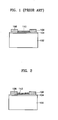
- a conventional carbon nanotube field effect transistor includes a layer of p -doped silicon 102 which forms a back gate for the device.
- An insulative layer 104 of silicon dioxide SiO 2 is provided above the back gate 102 with a source electrode 106 (which has been labeled "S") provided above the layer 104 of silicon dioxide.
- a drain electrode 108 is also provided above the layer 104 of silicon dioxide.
- a carbon nanotube 110 (not drawn to scale in Fig. 1 or in the other figures for ease of understanding) is provided between the source 106 and the drain 108 with the carbon nanotube 110 in electrical contact with both the source electrode 106 and with the drain electrode 108.
- CNT FET carbon nanotube field effect transistor
- the physical device structure of a CNT FET of Fig. 1 is inverted (or "upside down") with respect to the typical physical device structure of a silicon FET.
- the source and drain are above the gate in the CNT FET rather than having the gate above the source and drain as in a conventional silicon FET.
- the channel between the source and drain is provided by the carbon nanotube instead of by a single crystal of silicon.
- the carbon nanotube and the source and drain are provided above the gate, it is believed that the source and drain could be below the gate or that the carbon nanotube could be buried within the device structure.
- the substrate of the CNT FET could be a layer of silicon with a separate gate provided above the source and drain or with a multi-gate arrangement.
- the present invention is not limited to use with the CNT FET of Fig. 1 but instead is believed to be usable with all FETs having a channel provided by a nanotube or nanowire.
- the source and drain electrodes are typically comprised of metal(s) although the source and drain electrodes could also be comprised of polysilicon which has been doped to act as a conductor.
- the substrate which forms the back gate 102 is typically comprised of silicon although the substrate may be comprised of any material which provides a functional gate for the CNT FET.
- the oxide layer above the gate 102 is preferably comprised of silicon dioxide although the oxide layer may be comprised of any suitable, conventional material, such as another oxide material.
- the oxide/insulative layer may be comprised of any suitable material having a relatively high index of dielectric constant ⁇ .
- a relatively high index of dielectric constant ⁇ generally means a value for ⁇ which is higher than the index of dielectric constant ⁇ value of SiO 2 of about 4.0.
- the nanotube is preferably comprised of carbon as conventionally known although the nanotube may be comprised of other materials.
- the nanotube 110 in devices according to the present invention may be a single wall carbon nanotube (SWCNT) or a double wall carbon nanotube (DWCNT) or bundles of such nanotubes, as desired.
- a nanowire may be used for the nanotube 110.
- the nanotube may comprise any material which forms a Schottky barrier, with the energy of the Schottky barrier being changeable through the presence of a carrier-trapping material such as oxygen molecules which has been adsorbed by the material.
- the carrier-trapping material preferably has a Lowest Unoccupied Molecular Level or LUMO which is within the band gap of the channel material, i.e., the nanotube. If the LUMO value of the carrier-trapping material is below the Fermi level of the channel material, holes would be trapped as the carriers.
- the conventional CNT FETs are ambipolar devices. Although only a typical, single gate CNT FET device is illustrated, the present invention may be used in any type of FET design which is conducive to the use of carbon nanotubes such as multigate or multiwalled FETs as well as FETs in which the CNT is suspended between the source and drain electrodes.
- the CNT serves as the channel instead of a single crystal of silicon.
- the CNT may also be buried in the device.
- a junction typically does not exist between the CNT and the metal electrodes but instead an interface is provided between the CNT and the source electrode and the drain electrode.
- the gate may be provided above or below the CNT.
- a nanotube field effect transistor corresponds generally to the conventional devices such as is shown in connection with Fig. 1.
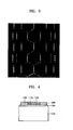
- the nanotube field effect transistor of Fig. 2 includes a layer of p- doped silicon 102 which forms a gate for the device.
- the layer 102 in the exemplary embodiment is a single crystal of silicon which has been highly doped to act as a back gate for the device, as conventionally known in the art.
- An insulative layer 104 of silicon dioxide SiO 2 is provided above the doped substrate 102 with a source electrode 106 provided above the layer 104 of silicon dioxide.
- a drain electrode 108 is provided above the layer 104 of silicon dioxide.
- the source electrode 106 and the drain electrode 108 are preferably comprised of metal such as titanium, molybdenum, or gold or alloys of those elements.
- the electrodes 106 and 108 may also be comprised of polysilicon which has been doped to function as a conductor.
- a carbon nanotube 110 (not drawn to scale) extends between the source electrode 106 and the drain electrode 108 with the carbon nanotube 110 in electrical contact both with the source electrode 106 and with the drain electrode 108.
- the carbon nanotube field effect transistor (CNT FET) differs from the conventional carbon nanotube field effect transistor in that a carrier-trapping material 112 is provided for the nanotube.
- the carner-trapping material comprises molecules of oxygen molecules (O 2 ).
- the oxygen molecules is adsorbed by the nanotube 110 during fabrication of the CNT FET.
- the presence of the carrier-trapping material such as oxygen molecules suppresses electron injection from the drain electrode which changes the conventional CNT FET from an ambipolar device to a unipolar CNT FET device.
- the presence of the carrier-trapping material provides a LUMO (lowest unoccupied molecular level) roughly in the middle of the CNT energy gap (see also Figs. 6a-6c discussed below).
- the LUMO level of the O 2 molecules is provided by the Opp ⁇ * orbital level of the oxygen atom.
- the oxygen molecules or other carrier-trapping material trap electrons from the drain electrode.
- the whole band both conduction band as well as valence band
- the energy barrier for electron injection increases which causes the CNT FET to be unipolar rather than ambipolar.
- the carbon nanotube is exposed to oxygen molecules (O 2 ) preferably under sufficient pressure to facilitate the adsorption of the oxygen molecules by the nanotube so that the oxygen molecules adhere to the carbon nanotube.
- Oxygen molecules are stable up to about 200°C which may be unsuitable for some semiconductor fabrication steps.
- the carrier-trapping material may be another material besides oxygen molecules (with a higher temperature level tolerance) so long as the material has a LUMO (lowest unoccupied molecular level) which is within the band gap of the channel material, i.e., roughly equal to the Fermi level of the CNT.
- the channel between the source and drain is provided by the carbon nanotube instead of by a silicon single crystal.
- the carbon nanotube and the source and drain electrodes are provided above the gate, the present invention is applicable to devices in which the source and drain electrodes are provided below the gate and where the carbon nanotube is buried within the device structure.
- the substrate of the CNT FET could be a layer of silicon with a separate gate provided above the source and drain electrodes or with a multi-gate arrangement as conventionally known for CNT FETs.
- the source and drain electrodes are typically comprised of metal(s) although the source and drain electrodes could also be comprised of polysilicon which has been sufficiently doped to function as a conductor.
- the substrate which forms the gate 102 is typically comprised of silicon although the substrate may be comprised of any material which provides a gate for the CNT FET.
- the oxide layer 104 above the gate 102 is preferably comprised of silicon dioxide although the oxide layer may be comprised of any suitable insulative material, and preferably of an oxide material.
- the nanotube is preferably comprised of carbon as conventionally known although the nanotube may be comprised of other materials.
- the adsorption of oxygen molecules by the carbon nanotube is illustrated with the individual atoms of oxygen held by adjacent atoms of carbon in the nanotube.
- the oxygen atoms facilitate carrier-trapping in the nanotube.
- the carrier-trapping material such as oxygen molecules is adsorbed by the nanotube
- the carrier-trapping material may also be adsorbed by the insulative layer 104, such as the layer of SiO 2 .
- the oxygen molecules may be adsorbed on the surface of the CNT as well as on the inside of the CNT.
- the carrier-trapping material such as oxygen molecules may be adsorbed on the insulative layer of SiO 2 which is physically near to the CNT and thereby render the device unipolar.
- the carrier-trapping material may also be provided in an additional layer 105 which is applied as a spin-coat on the device or which is deposited in any suitable conventional way for semiconductor device fabrication.
- the carrier-trapping material may be provided in the material of the additional layer 105 as applied to the device or the carrier-trapping material may be adsorbed by the layer in a subsequent processing step during fabrication.
- the additional layer 105 may be comprised of any suitable material which can adsorb or contain the carrier-trapping material, such as oxygen molecules.
- the additional layer 105 may be a protective layer for the device, especially a layer which is applied during a relatively low temperature fabrication process
- the gap between the CNT and the material with the carrier-trapping material be less than about 1 nm (i.e., less than the quantum length of electron travel).
- the additional layer of material 105 may be provided during manufacture of the CNT FET either physically above or below the carbon nanotube or both (i.e., to enclose the nanotube).
- the additional layer 105 may also be provided either before or after the carbon nanotube has been provided between the source electrode 106 and the drain electrode 108.
- a graph of the Energy-K (i.e., the wave vector) at zero gate voltage is shown in a conventional CNT FET (i.e., without the use of a carrier-trapping material such as oxygen molecules).
- the lower curve represents the HOMO (or highest occupied molecular level) and the upper curve represents the LUMO (or lowest unoccupied molecular level) for the CNT channel in a conventional CNT FET.
- a graph of the Energy-K (i.e., the wave vector) at zero gate voltage is shown in a CNT FET according to an embodiment of the present invention in which a carrier-trapping material such as oxygen molecules has been adsorbed by the CNT.
- CMOS devices and logic gates which comprise CNT FETs generally require either n or p transistor devices (i.e., devices which are unipolar) and which operate at the same gate bias.
- Conventional CNT FETs demonstrate ambiopolar characteristics as a result of the injection of carriers from a lowering of the barriers in either the source or the drain.
- the band alignment at different bias conditions of the gate are shown.
- the energy of a hole injection is plotted at different voltages as a function of position along the carbon nanotube. The energy is provided in electron-volts (eV) and the position is shown in nanometers (nm).
- Fermi level 220 of the CNT is shown as a dashed line between the LUMO level 212 of the CNT and the HOMO level 214 of the CNT.
- the LUMO level 216 of the oxygen molecules is roughly midway between the LUMO level 212 and the HOMO level 214 of the CNT.
- a nanotube field effect transistor is converted from an ambipolar device to a unipolar device by providing a carrier-trapping material such as oxygen molecules for the nanotube.
- the carrier-trapping material is preferably adsorbed by the nanotube by subjecting the nanotube to oxygen molecules under suitable pressure and at a temperature which facilitates the adsorption of the material by the nanotube.
- the carrier-trapping material may be provided in the insulative layer of the device (such as a layer of SiO 2 ). Alternatively (or in addition thereto) another layer can be spun-on or deposited above or below the CNT during fabrication of the device. If the carrier-trapping material is not provided in the additional layer during fabrication, then the device is again exposed to the carrier-trapping material (such as O 2 ) during fabrication to enable the carrier-trapping material to be adsorbed by the additional layer.
- the insulative layer or additional layer containing the carrier-trapping material is close to or touching the CNT so that any gap between the CNT and the material containing the carrier-trapping material is less than about 1 nanometer (or the quantum length of electron travel).
Landscapes
- Engineering & Computer Science (AREA)
- Chemical & Material Sciences (AREA)
- Nanotechnology (AREA)
- Physics & Mathematics (AREA)
- Mathematical Physics (AREA)
- Theoretical Computer Science (AREA)
- Crystallography & Structural Chemistry (AREA)
- Thin Film Transistor (AREA)
- Carbon And Carbon Compounds (AREA)
Applications Claiming Priority (2)
| Application Number | Priority Date | Filing Date | Title |
|---|---|---|---|
| KR20040081751 | 2004-10-13 | ||
| KR1020050063305A KR100647330B1 (ko) | 2004-10-13 | 2005-07-13 | 캐리어 트래핑 물질을 구비한 유니폴라 나노튜브트랜지스터 및 그 제조방법 |
Publications (2)
| Publication Number | Publication Date |
|---|---|
| EP1648041A2 true EP1648041A2 (de) | 2006-04-19 |
| EP1648041A3 EP1648041A3 (de) | 2008-08-27 |
Family
ID=35696007
Family Applications (1)
| Application Number | Title | Priority Date | Filing Date |
|---|---|---|---|
| EP05256381A Withdrawn EP1648041A3 (de) | 2004-10-13 | 2005-10-13 | Unipolarer Nanoröhrchen-Transistor mit Ladungsträgerfangstellenmaterial |
Country Status (4)
| Country | Link |
|---|---|
| US (1) | US20070246784A1 (de) |
| EP (1) | EP1648041A3 (de) |
| JP (1) | JP2006114912A (de) |
| CN (1) | CN100481502C (de) |
Families Citing this family (19)
| Publication number | Priority date | Publication date | Assignee | Title |
|---|---|---|---|---|
| US7999251B2 (en) * | 2006-09-11 | 2011-08-16 | International Business Machines Corporation | Nanowire MOSFET with doped epitaxial contacts for source and drain |
| KR101227144B1 (ko) | 2006-12-13 | 2013-01-28 | 엘지디스플레이 주식회사 | 박막 트랜지스터 및 이의 제조 방법 |
| US8563380B2 (en) * | 2008-01-07 | 2013-10-22 | Shachar Richter | Electric nanodevice and method of manufacturing same |
| KR102108121B1 (ko) | 2013-06-10 | 2020-05-08 | 삼성디스플레이 주식회사 | 박막 트랜지스터 기판 |
| US9455421B2 (en) | 2013-11-21 | 2016-09-27 | Atom Nanoelectronics, Inc. | Devices, structures, materials and methods for vertical light emitting transistors and light emitting displays |
| US9203041B2 (en) * | 2014-01-31 | 2015-12-01 | International Business Machines Corporation | Carbon nanotube transistor having extended contacts |
| US9786853B2 (en) | 2014-02-11 | 2017-10-10 | Wisconsin Alumni Research Foundation | Floating evaporative assembly of aligned carbon nanotubes |
| US9368723B2 (en) * | 2014-02-11 | 2016-06-14 | Wisconsin Alumni Research Foundation | Dose-controlled, floating evaporative assembly of aligned carbon nanotubes for use in high performance field effect transistors |
| US9425405B1 (en) * | 2015-02-11 | 2016-08-23 | Wisconsin Alumni Research Foundation | Continuous, floating evaporative assembly of aligned carbon nanotubes |
| CN105336792B (zh) * | 2015-11-02 | 2019-03-01 | 京东方科技集团股份有限公司 | 碳纳米管半导体器件及其制备方法 |
| US10957868B2 (en) | 2015-12-01 | 2021-03-23 | Atom H2O, Llc | Electron injection based vertical light emitting transistors and methods of making |
| US10541374B2 (en) | 2016-01-04 | 2020-01-21 | Carbon Nanotube Technologies, Llc | Electronically pure single chirality semiconducting single-walled carbon nanotube for large scale electronic devices |
| CN108336226B (zh) * | 2017-01-20 | 2020-03-17 | 清华大学 | 薄膜晶体管 |
| US10873026B2 (en) | 2017-03-10 | 2020-12-22 | Wisconsin Alumni Research Foundation | Alignment of carbon nanotubes in confined channels |
| US10847757B2 (en) | 2017-05-04 | 2020-11-24 | Carbon Nanotube Technologies, Llc | Carbon enabled vertical organic light emitting transistors |
| US10665796B2 (en) | 2017-05-08 | 2020-05-26 | Carbon Nanotube Technologies, Llc | Manufacturing of carbon nanotube thin film transistor backplanes and display integration thereof |
| US10978640B2 (en) | 2017-05-08 | 2021-04-13 | Atom H2O, Llc | Manufacturing of carbon nanotube thin film transistor backplanes and display integration thereof |
| KR20210134616A (ko) | 2019-01-04 | 2021-11-10 | 아톰 에이치투오, 엘엘씨 | 탄소 나노튜브 기반 무선 주파수 장치 |
| US11165032B2 (en) * | 2019-09-05 | 2021-11-02 | Taiwan Semiconductor Manufacturing Co., Ltd. | Field effect transistor using carbon nanotubes |
Family Cites Families (11)
| Publication number | Priority date | Publication date | Assignee | Title |
|---|---|---|---|---|
| US6423583B1 (en) * | 2001-01-03 | 2002-07-23 | International Business Machines Corporation | Methodology for electrically induced selective breakdown of nanotubes |
| JP2003017508A (ja) * | 2001-07-05 | 2003-01-17 | Nec Corp | 電界効果トランジスタ |
| KR100426495B1 (ko) * | 2001-12-28 | 2004-04-14 | 한국전자통신연구원 | 단일 탄소 나노튜브를 이용한 반도체 소자 및 그 제조 방법 |
| US6891227B2 (en) * | 2002-03-20 | 2005-05-10 | International Business Machines Corporation | Self-aligned nanotube field effect transistor and method of fabricating same |
| JP4974263B2 (ja) * | 2002-05-20 | 2012-07-11 | 富士通株式会社 | 半導体装置の製造方法 |
| TWI222742B (en) * | 2003-05-05 | 2004-10-21 | Ind Tech Res Inst | Fabrication and structure of carbon nanotube-gate transistor |
| EP1634296A4 (de) * | 2003-06-09 | 2007-02-14 | Nantero Inc | Nichtflüchtige elektromechanische feldeffektbausteine und schaltungen damit und verfahren zu ihrer herstellung |
| JP4228204B2 (ja) * | 2003-07-07 | 2009-02-25 | セイコーエプソン株式会社 | 有機トランジスタの製造方法 |
| TWI253502B (en) * | 2003-08-26 | 2006-04-21 | Ind Tech Res Inst | A structure and manufacturing process of a nano device transistor for a biosensor |
| KR100601965B1 (ko) * | 2004-10-02 | 2006-07-18 | 삼성전자주식회사 | n형 탄소 나노튜브를 구비한 n형 탄소나노튜브 전계효과트랜지스터 및 그 제조방법 |
| US7582534B2 (en) * | 2004-11-18 | 2009-09-01 | International Business Machines Corporation | Chemical doping of nano-components |
-
2005
- 2005-08-29 US US11/212,582 patent/US20070246784A1/en not_active Abandoned
- 2005-10-12 CN CNB2005101067809A patent/CN100481502C/zh not_active Expired - Fee Related
- 2005-10-13 JP JP2005298837A patent/JP2006114912A/ja not_active Withdrawn
- 2005-10-13 EP EP05256381A patent/EP1648041A3/de not_active Withdrawn
Non-Patent Citations (1)
| Title |
|---|
| YU-MING LIN; JOERG APPENZELLER; PHAEDON AVOURIS: "Ambipolar-to-Unipolar Conversion of Carbon Nanotube Transistors by Gate Structure Engineering", NANO LETTERS, vol. 4, no. 5, 2004, pages 947 - 950 |
Also Published As
| Publication number | Publication date |
|---|---|
| US20070246784A1 (en) | 2007-10-25 |
| EP1648041A3 (de) | 2008-08-27 |
| CN100481502C (zh) | 2009-04-22 |
| CN1770467A (zh) | 2006-05-10 |
| JP2006114912A (ja) | 2006-04-27 |
Similar Documents
| Publication | Publication Date | Title |
|---|---|---|
| EP1648041A2 (de) | Unipolarer Nanoröhrchen-Transistor mit Ladungsträgerfangstellenmaterial | |
| Wind et al. | Vertical scaling of carbon nanotube field-effect transistors using top gate electrodes | |
| Wind et al. | Fabrication and electrical characterization of top gate single-wall carbon nanotube field-effect transistors | |
| Lin et al. | High-performance carbon nanotube field-effect transistor with tunable polarities | |
| Chen et al. | Self-aligned carbon nanotube transistors with charge transfer doping | |
| US7170120B2 (en) | Carbon nanotube energy well (CNEW) field effect transistor | |
| Avouris et al. | Carbon nanotube transistors and logic circuits | |
| Chen et al. | Electric-field-dependent charge-carrier velocity in semiconducting carbon nanotubes | |
| TWI463654B (zh) | 奈米管/奈米導線場效電晶體之自行對準製程 | |
| JP4717855B2 (ja) | 静電的に制御されるトンネリング・トランジスタ | |
| US20110089404A1 (en) | Microfabrication of Carbon-based Devices Such as Gate-Controlled Graphene Devices | |
| KR102075804B1 (ko) | 그래핀-계 반도체 소자 | |
| US20080251862A1 (en) | Accumulation field effect microelectronic device and process for the formation thereof | |
| Appenzeller et al. | Dual-gate silicon nanowire transistors with nickel silicide contacts | |
| Antonova | Vertical heterostructures based on graphene and other 2D materials | |
| KR20000034979A (ko) | 마이크로전자 디바이스 | |
| US9209246B2 (en) | Accumulation field effect microelectronic device and process for the formation thereof | |
| Avouris et al. | Carbon nanotube electronics and optoelectronics | |
| US20140287575A1 (en) | Spatial orientation of the carbon nanotubes in electrophoretic deposition process | |
| Tang et al. | Carbon nanotube complementary logic with low-temperature processed end-bonded metal contacts | |
| Mei et al. | Two-dimensional vertical transistor with one-dimensional van der Waals contact | |
| KR100647330B1 (ko) | 캐리어 트래핑 물질을 구비한 유니폴라 나노튜브트랜지스터 및 그 제조방법 | |
| Ramezani et al. | Fundamental phenomena in nanoscale semiconductor devices | |
| Moriyama et al. | High-performance top-gate carbon nanotube field-effect transistors and complementary metal–oxide–semiconductor inverters realized by controlling interface charges | |
| Park et al. | Formation of a quantum dot in a single-walled carbon nanotube using the Al top-gates |
Legal Events
| Date | Code | Title | Description |
|---|---|---|---|
| PUAI | Public reference made under article 153(3) epc to a published international application that has entered the european phase |
Free format text: ORIGINAL CODE: 0009012 |
|
| 17P | Request for examination filed |
Effective date: 20051026 |
|
| AK | Designated contracting states |
Kind code of ref document: A2 Designated state(s): AT BE BG CH CY CZ DE DK EE ES FI FR GB GR HU IE IS IT LI LT LU LV MC NL PL PT RO SE SI SK TR |
|
| AX | Request for extension of the european patent |
Extension state: AL BA HR MK YU |
|
| RIN1 | Information on inventor provided before grant (corrected) |
Inventor name: PARK, NOE-JUNG Inventor name: PARK, WAN-JUN Inventor name: KANG, DONG-HUN |
|
| PUAL | Search report despatched |
Free format text: ORIGINAL CODE: 0009013 |
|
| RIC1 | Information provided on ipc code assigned before grant |
Ipc: H01L 51/05 20060101ALI20080716BHEP Ipc: H01L 51/30 20060101ALI20080716BHEP Ipc: H01L 29/10 20060101ALI20080716BHEP Ipc: H01L 29/06 20060101ALI20080716BHEP Ipc: H01L 29/78 20060101AFI20080716BHEP |
|
| AK | Designated contracting states |
Kind code of ref document: A3 Designated state(s): AT BE BG CH CY CZ DE DK EE ES FI FR GB GR HU IE IS IT LI LT LU LV MC NL PL PT RO SE SI SK TR |
|
| AX | Request for extension of the european patent |
Extension state: AL BA HR MK YU |
|
| 17Q | First examination report despatched |
Effective date: 20090212 |
|
| AKX | Designation fees paid |
Designated state(s): DE FR GB |
|
| STAA | Information on the status of an ep patent application or granted ep patent |
Free format text: STATUS: THE APPLICATION IS DEEMED TO BE WITHDRAWN |
|
| 18D | Application deemed to be withdrawn |
Effective date: 20090623 |