EP1643553A2 - Kupferner Zwischenträger zur Verringerung der Verbiegung von Chipstapeln sowie Herstellung von Chipstapeln - Google Patents
Kupferner Zwischenträger zur Verringerung der Verbiegung von Chipstapeln sowie Herstellung von Chipstapeln Download PDFInfo
- Publication number
- EP1643553A2 EP1643553A2 EP05255975A EP05255975A EP1643553A2 EP 1643553 A2 EP1643553 A2 EP 1643553A2 EP 05255975 A EP05255975 A EP 05255975A EP 05255975 A EP05255975 A EP 05255975A EP 1643553 A2 EP1643553 A2 EP 1643553A2
- Authority
- EP
- European Patent Office
- Prior art keywords
- integrated circuit
- die
- substrate
- interposer
- copper
- Prior art date
- Legal status (The legal status is an assumption and is not a legal conclusion. Google has not performed a legal analysis and makes no representation as to the accuracy of the status listed.)
- Ceased
Links
Images

Classifications
-
- H—ELECTRICITY
- H10—SEMICONDUCTOR DEVICES; ELECTRIC SOLID-STATE DEVICES NOT OTHERWISE PROVIDED FOR
- H10W—GENERIC PACKAGES, INTERCONNECTIONS, CONNECTORS OR OTHER CONSTRUCTIONAL DETAILS OF DEVICES COVERED BY CLASS H10
- H10W90/00—Package configurations
-
- H—ELECTRICITY
- H10—SEMICONDUCTOR DEVICES; ELECTRIC SOLID-STATE DEVICES NOT OTHERWISE PROVIDED FOR
- H10W—GENERIC PACKAGES, INTERCONNECTIONS, CONNECTORS OR OTHER CONSTRUCTIONAL DETAILS OF DEVICES COVERED BY CLASS H10
- H10W72/00—Interconnections or connectors in packages
- H10W72/071—Connecting or disconnecting
- H10W72/072—Connecting or disconnecting of bump connectors
-
- H—ELECTRICITY
- H10—SEMICONDUCTOR DEVICES; ELECTRIC SOLID-STATE DEVICES NOT OTHERWISE PROVIDED FOR
- H10W—GENERIC PACKAGES, INTERCONNECTIONS, CONNECTORS OR OTHER CONSTRUCTIONAL DETAILS OF DEVICES COVERED BY CLASS H10
- H10W72/00—Interconnections or connectors in packages
- H10W72/071—Connecting or disconnecting
- H10W72/073—Connecting or disconnecting of die-attach connectors
-
- H—ELECTRICITY
- H10—SEMICONDUCTOR DEVICES; ELECTRIC SOLID-STATE DEVICES NOT OTHERWISE PROVIDED FOR
- H10W—GENERIC PACKAGES, INTERCONNECTIONS, CONNECTORS OR OTHER CONSTRUCTIONAL DETAILS OF DEVICES COVERED BY CLASS H10
- H10W72/00—Interconnections or connectors in packages
- H10W72/20—Bump connectors, e.g. solder bumps or copper pillars; Dummy bumps; Thermal bumps
- H10W72/251—Materials
- H10W72/252—Materials comprising solid metals or solid metalloids, e.g. PbSn, Ag or Cu
-
- H—ELECTRICITY
- H10—SEMICONDUCTOR DEVICES; ELECTRIC SOLID-STATE DEVICES NOT OTHERWISE PROVIDED FOR
- H10W—GENERIC PACKAGES, INTERCONNECTIONS, CONNECTORS OR OTHER CONSTRUCTIONAL DETAILS OF DEVICES COVERED BY CLASS H10
- H10W72/00—Interconnections or connectors in packages
- H10W72/30—Die-attach connectors
- H10W72/351—Materials of die-attach connectors
- H10W72/353—Materials of die-attach connectors not comprising solid metals or solid metalloids, e.g. ceramics
- H10W72/354—Materials of die-attach connectors not comprising solid metals or solid metalloids, e.g. ceramics comprising polymers
-
- H—ELECTRICITY
- H10—SEMICONDUCTOR DEVICES; ELECTRIC SOLID-STATE DEVICES NOT OTHERWISE PROVIDED FOR
- H10W—GENERIC PACKAGES, INTERCONNECTIONS, CONNECTORS OR OTHER CONSTRUCTIONAL DETAILS OF DEVICES COVERED BY CLASS H10
- H10W72/00—Interconnections or connectors in packages
- H10W72/851—Dispositions of multiple connectors or interconnections
- H10W72/874—On different surfaces
- H10W72/877—Bump connectors and die-attach connectors
-
- H—ELECTRICITY
- H10—SEMICONDUCTOR DEVICES; ELECTRIC SOLID-STATE DEVICES NOT OTHERWISE PROVIDED FOR
- H10W—GENERIC PACKAGES, INTERCONNECTIONS, CONNECTORS OR OTHER CONSTRUCTIONAL DETAILS OF DEVICES COVERED BY CLASS H10
- H10W90/00—Package configurations
- H10W90/20—Configurations of stacked chips
- H10W90/231—Configurations of stacked chips the stacked chips being on both top and bottom sides of an auxiliary carrier having no electrical connection structure
-
- H—ELECTRICITY
- H10—SEMICONDUCTOR DEVICES; ELECTRIC SOLID-STATE DEVICES NOT OTHERWISE PROVIDED FOR
- H10W—GENERIC PACKAGES, INTERCONNECTIONS, CONNECTORS OR OTHER CONSTRUCTIONAL DETAILS OF DEVICES COVERED BY CLASS H10
- H10W90/00—Package configurations
- H10W90/20—Configurations of stacked chips
- H10W90/288—Configurations of stacked chips characterised by arrangements for thermal management of the stacked chips
-
- H—ELECTRICITY
- H10—SEMICONDUCTOR DEVICES; ELECTRIC SOLID-STATE DEVICES NOT OTHERWISE PROVIDED FOR
- H10W—GENERIC PACKAGES, INTERCONNECTIONS, CONNECTORS OR OTHER CONSTRUCTIONAL DETAILS OF DEVICES COVERED BY CLASS H10
- H10W90/00—Package configurations
- H10W90/701—Package configurations characterised by the relative positions of pads or connectors relative to package parts
- H10W90/721—Package configurations characterised by the relative positions of pads or connectors relative to package parts of bump connectors
- H10W90/724—Package configurations characterised by the relative positions of pads or connectors relative to package parts of bump connectors between a chip and a stacked insulating package substrate, interposer or RDL
-
- H—ELECTRICITY
- H10—SEMICONDUCTOR DEVICES; ELECTRIC SOLID-STATE DEVICES NOT OTHERWISE PROVIDED FOR
- H10W—GENERIC PACKAGES, INTERCONNECTIONS, CONNECTORS OR OTHER CONSTRUCTIONAL DETAILS OF DEVICES COVERED BY CLASS H10
- H10W90/00—Package configurations
- H10W90/701—Package configurations characterised by the relative positions of pads or connectors relative to package parts
- H10W90/731—Package configurations characterised by the relative positions of pads or connectors relative to package parts of die-attach connectors
- H10W90/736—Package configurations characterised by the relative positions of pads or connectors relative to package parts of die-attach connectors between a chip and a stacked lead frame, conducting package substrate or heat sink
Definitions
- the present invention relates generally to integrated circuit (IC) packages and, more specifically, to a stacked die ID package using a copper interposer to reduce warping of a substrate.
- IC integrated circuit
- SoC system-on-a-chip
- manufacturers are also packing as many IC dies as possible onto circuit board.
- manufactures place IC dies as close together as possible on a substrate to thereby increase IC die density.
- manufacturers also stack IC dies vertically in order to improve the packing density of the integrated circuit dies.
- a first IC die is mounted on a substrate by means of, for example, a solder ball grid array (BGA).
- BGA solder ball grid array
- a silicon (Si) interposer mounted on top of the first IC die by means of an attachment layer, such as an adhesive layer or die attach.
- a second IC die is then mounted on top of the silicon interposer by means of another attachment layer (i.e., another adhesive layer/die attach). Additional IC dies and silicon interposers may subsequently be added to the stack to further improve packing density.
- Such a stack of IC chips may be implemented on an open substrate or within a sealed IC package.
- solder joint reliability SJR
- solder joints frequently crack due to thermal stresses encountered during manufacturing or during operation. Alternate cycles of heating and cooling may cause the substrate to warp, particularly as a result of shrinkage that occurs as the substrate cools.
- the coefficient of thermal expansion (CTE) of a silicon die is significantly less than the CTE of a substrate.
- the solder joints of a ball grid array connecting an IC die to a substrate are very fine. As the substrate warps, some of the solder joints may crack, thereby causing defects. This substrate warping is particularly damaging to stacked assemblies of integrated circuit dies.
- the present invention provides a copper interposer that reduces the warping of a stacked die integrated circuit (IC) package caused by the warping of the substrate due to thermal changes in the substrate.
- the copper (Cu) interposer has a significantly higher coefficient of thermal expansion (CTE) than a conventional silicon (Si) interposer. The higher CTE enables the copper interposer to counteract the substrate shrinkage more effectively.
- It is a primary object of the present invention to provide a stacked die integrated circuit assembly comprising: 1) a substrate; 2) a first integrated circuit die mounted on the substrate; 3) a copper interposer mounted on the first integrated circuit die; and 4) a second integrated circuit die mounted on the copper interposer.
- a coefficient of thermal expansion associated with the copper interposer is more closely matched to a coefficient of thermal expansion of the substrate than a coefficient of thermal expansion of a silicon interposer.
- the method comprises the steps of 1) attaching a lower surface of a first integrated circuit die to a substrate; 2) attaching a lower surface of a copper interposer to an upper surface of the first integrated circuit die; and 3) attaching a lower surface of a second integrated circuit die to an upper surface of the copper interposer.
- the lower surface of the first integrated circuit die is attached to the substrate using a solder ball grid array
- the lower surface of the copper interposer is attached to the upper surface of the first integrated circuit die using a first adhesive layer
- the lower surface of the second integrated circuit die is attached to the upper surface of the copper interposer using a second adhesive layer.
- FIGURE 1 illustrates a top view of an exemplary electronic assembly board on which is disposed stacked die integrated circuits according to the principles of the present invention
- FIGURE 2A illustrates a cross-sectional view of an exemplary stacked die integrated circuit using only a single die according to one embodiment of the present invention
- FIGURE 2B illustrates a cross-sectional view of an exemplary stacked die integrated circuit using two dies according to another embodiment of the present invention
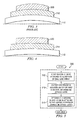
- FIGURE 3 illustrates the warping of an exemplary stacked die integrated circuit assembly containing a PRIOR ART silicon interposer
- FIGURE 4 illustrates the warping of an exemplary stacked die assembly containing a copper interposer according to the principles of the present invention.
- FIGURE 5 is a flow diagram illustrating an exemplary process for making a stacked die assembly containing a copper interposer according to the principles of the present invention.
- FIGURES 1 through 5 discussed below, and the various embodiments used to describe the principles of the present invention in this patent document are by way of illustration only and should not be construed in any way to limit the scope of the invention. Those skilled in the art will understand that the principles of the present invention may be implemented in any suitably arranged stacked die integrated circuit assembly.
- FIGURE 1 is a top view of exemplary electronic assembly board 100, on which is disposed a plurality of stacked die integrated circuits according to the principles of the present invention.
- Electronic assembly board 100 comprises substrate 110, which provides support and electrical connections for a block of stacked die ball grid array (SDBGA) integrated circuit assemblies, which are arbitrarily labeled SDBGA 1 through SDBGA 12, respectively.
- Stacked die integrated circuit (IC) assembly 120 labeled SDBGA 1, is a representative one of SDGA 1 through SDBGA 12.
- Stacked die IC assembly 120 comprises one or more silicon (Si) dies (or wafers) that are vertically stacked on substrate 110.
- a first silicon IC die is attached to substrate 110 by means of a grid array of solder balls that also provide electrical connection paths between electronic pads on the lower surface of the first silicon IC die and electronic pads on the upper surface of substrate 110.
- a copper interposer according to the present invention is then mounted on the upper surface of the first silicon IC day by means of a die attach (or adhesive layer). Additional layers of IC dies an interposers may also be added.
- the use of a copper interposer in lieu of a silicon interposer improves solder joint reliability (SJR) by reducing the warping of the substrate caused by thermal changes.
- the coefficient of thermal expansion (CTE) of a copper interposer e.g., 17.7 ppm/°C
- the CTE of a silicon interposer e.g., 2.8 ppm/°C
- the higher CTE of copper is much closer to the CTE of a typical substrate (e.g., 18 ppm/°C). This helps to counteract the substrate shrinkage.
- FIGURE 2A is a cross-sectional view of an exemplary stacked die integrated circuit (IC) assembly 120 that uses only a single die according to one embodiment of the present invention.
- Stacked die IC assembly 120 comprises substrate 110, silicon (Si) integrated circuit (IC) die 210, and copper (Cu) interposer 220.
- Silicon IC die 210 is mounted on substrate 110 by means of solder ball grid array 201.
- Copper interposer 220 is mounted on silicon IC die 210 by means of adhesive layer 202 (i.e. , a die attach layer).
- copper interposer 220 still reduces warping of substrate 110 due to thermal change. Additional silicon IC dies may subsequently be mounted on the upper surface of copper interposer 220.
- FIGURE 2B is a cross-sectional view of an exemplary stacked die integrated circuit (IC) assembly 120 using two dies according to another embodiment of the present invention.
- Stacked die IC assembly 120 comprises substrate 110, silicon (Si) integrated (IC) die 210, copper (Cu) interposer 220, and silicon (Si) integrated (IC) assembly 230.
- silicon IC die 210 is mounted on substrate 110 by means of solder ball grid array 201 and copper interposer 220 is mounted on silicon IC die 210 by means of adhesive layer 202 ((i.e., die attach).
- silicon IC die 230 is mounted on copper interposer 220 by means of adhesive layer 203. Additional layers of copper interposers and silicon IC dies may subsequently be mounted on the upper surface of silicon IC die 230.
- FIGURE 3 illustrates the warping of an exemplary stacked die integrated circuit assembly containing PRIOR ART silicon (Si) interposer 300.
- FIGURE 4 illustrates warping of an exemplary stacked die assembly containing copper interposer 230 according to the principles of the present invention.
- the components illustrated in FIGURES 3 and 4 are not intended to be drawn to scale.
- the dotted lines in FIGURES 3 and 4 are straight lines indicating the relative amounts of warping that occur with a silicon interposer and a copper interposer.
- FIGURES 3 and 4 are intended to illustrate that there is relatively less warping (or warpage) of the substrate and integrated circuit die when copper interposer 220 is used (in FIGURE 4) than when silicon interposer 300 is used (FIGURE 3).
- FIGURE 5 depicts flow diagram 500, which illustrates an exemplary process for making a stacked die assembly containing a copper interposer according to the principles of the present invention.
- a first silicon IC die is mounted on a substrate by means of a solder ball grid array (or any other similar or suitable interconnection layer; process step 505).
- a copper interposer is mounted on the first silicon IC die by means of a die attach layer (process step 510).
- a second silicon IC die is mounted on top of the copper interposer by means of another die attach layer (process step 515).
- Process steps 510 and 515 may then be repeated for additional layers of interposers and silicon IC dies.
Landscapes
- Die Bonding (AREA)
- Cooling Or The Like Of Semiconductors Or Solid State Devices (AREA)
Applications Claiming Priority (1)
| Application Number | Priority Date | Filing Date | Title |
|---|---|---|---|
| US10/954,630 US7196425B2 (en) | 2004-09-30 | 2004-09-30 | Copper interposer for reducing warping of integrated circuit packages and method of making IC packages |
Publications (2)
| Publication Number | Publication Date |
|---|---|
| EP1643553A2 true EP1643553A2 (de) | 2006-04-05 |
| EP1643553A3 EP1643553A3 (de) | 2006-11-22 |
Family
ID=35559376
Family Applications (1)
| Application Number | Title | Priority Date | Filing Date |
|---|---|---|---|
| EP05255975A Ceased EP1643553A3 (de) | 2004-09-30 | 2005-09-26 | Kupferner Zwischenträger zur Verringerung der Verbiegung von Chipstapeln sowie Herstellung von Chipstapeln |
Country Status (2)
| Country | Link |
|---|---|
| US (1) | US7196425B2 (de) |
| EP (1) | EP1643553A3 (de) |
Cited By (1)
| Publication number | Priority date | Publication date | Assignee | Title |
|---|---|---|---|---|
| US8178984B2 (en) | 2007-04-12 | 2012-05-15 | Micron Technology, Inc. | Flip chip with interposer |
Families Citing this family (7)
| Publication number | Priority date | Publication date | Assignee | Title |
|---|---|---|---|---|
| CN101652019B (zh) * | 2008-08-14 | 2011-07-27 | 富葵精密组件(深圳)有限公司 | 电路板预制品以及电路板组装方法 |
| US9159649B2 (en) * | 2011-12-20 | 2015-10-13 | Intel Corporation | Microelectronic package and stacked microelectronic assembly and computing system containing same |
| TWI444113B (zh) * | 2012-10-18 | 2014-07-01 | 同欣電子工業股份有限公司 | A circuit board with a hierarchical conductive unit |
| US9837352B2 (en) | 2015-10-07 | 2017-12-05 | Advanced Semiconductor Engineering, Inc. | Semiconductor device and method for manufacturing the same |
| US9852971B1 (en) | 2016-06-09 | 2017-12-26 | Advanced Semiconductor Engineering, Inc. | Interposer, semiconductor package structure, and semiconductor process |
| US10790232B2 (en) | 2018-09-15 | 2020-09-29 | International Business Machines Corporation | Controlling warp in semiconductor laminated substrates with conductive material layout and orientation |
| CN112151545B (zh) * | 2019-06-28 | 2024-05-14 | 西部数据技术公司 | 包括磁性压持层的半导体设备 |
Family Cites Families (13)
| Publication number | Priority date | Publication date | Assignee | Title |
|---|---|---|---|---|
| US6376904B1 (en) | 1999-12-23 | 2002-04-23 | Rambus Inc. | Redistributed bond pads in stacked integrated circuit die package |
| US6444921B1 (en) * | 2000-02-03 | 2002-09-03 | Fujitsu Limited | Reduced stress and zero stress interposers for integrated-circuit chips, multichip substrates, and the like |
| US6335491B1 (en) * | 2000-02-08 | 2002-01-01 | Lsi Logic Corporation | Interposer for semiconductor package assembly |
| TW498470B (en) | 2001-05-25 | 2002-08-11 | Siliconware Precision Industries Co Ltd | Semiconductor packaging with stacked chips |
| KR20030027413A (ko) | 2001-09-28 | 2003-04-07 | 삼성전자주식회사 | 칩 사이에 스페이서가 삽입된 멀티 칩 패키지와 그 제조방법 |
| US6737750B1 (en) * | 2001-12-07 | 2004-05-18 | Amkor Technology, Inc. | Structures for improving heat dissipation in stacked semiconductor packages |
| KR20030075860A (ko) * | 2002-03-21 | 2003-09-26 | 삼성전자주식회사 | 반도체 칩 적층 구조 및 적층 방법 |
| KR100429885B1 (ko) | 2002-05-09 | 2004-05-03 | 삼성전자주식회사 | 열방출 특성을 개선한 멀티 칩 패키지 |
| TW546795B (en) | 2002-06-04 | 2003-08-11 | Siliconware Precision Industries Co Ltd | Multichip module and manufacturing method thereof |
| US6773958B1 (en) * | 2002-10-17 | 2004-08-10 | Altera Corporation | Integrated assembly-underfill flip chip process |
| ITMI20022767A1 (it) * | 2002-12-24 | 2004-06-25 | St Microelectronics Srl | Processo per realizzare un dispositivo a semiconduttore |
| US6627990B1 (en) * | 2003-02-06 | 2003-09-30 | St. Assembly Test Service Ltd. | Thermally enhanced stacked die package |
| KR20040087501A (ko) * | 2003-04-08 | 2004-10-14 | 삼성전자주식회사 | 센터 패드 반도체 칩의 패키지 및 그 제조방법 |
-
2004
- 2004-09-30 US US10/954,630 patent/US7196425B2/en not_active Expired - Lifetime
-
2005
- 2005-09-26 EP EP05255975A patent/EP1643553A3/de not_active Ceased
Cited By (2)
| Publication number | Priority date | Publication date | Assignee | Title |
|---|---|---|---|---|
| US8178984B2 (en) | 2007-04-12 | 2012-05-15 | Micron Technology, Inc. | Flip chip with interposer |
| TWI411065B (zh) * | 2007-04-12 | 2013-10-01 | 美光科技公司 | 具有插入器之覆晶晶片,以及製造其之方法 |
Also Published As
| Publication number | Publication date |
|---|---|
| US20060071345A1 (en) | 2006-04-06 |
| EP1643553A3 (de) | 2006-11-22 |
| US7196425B2 (en) | 2007-03-27 |
Similar Documents
| Publication | Publication Date | Title |
|---|---|---|
| US5222014A (en) | Three-dimensional multi-chip pad array carrier | |
| US9385098B2 (en) | Variable-size solder bump structures for integrated circuit packaging | |
| CN108766940B (zh) | 用于3d封装的应力补偿层 | |
| US20080157327A1 (en) | Package on package structure for semiconductor devices and method of the same | |
| US5045922A (en) | Installation structure of integrated circuit devices | |
| JP2006502587A (ja) | マルチチップパッケージ用のコンポーネント、方法およびアセンブリ | |
| TWI492350B (zh) | 半導體封裝件及其製法 | |
| US11469152B2 (en) | Semiconductor chip package and fabrication method thereof | |
| US6888238B1 (en) | Low warpage flip chip package solution-channel heat spreader | |
| HK1004352B (en) | Stackable three-dimensional multiple chip semiconductor device and method for making the same | |
| US7439170B1 (en) | Design structure for final via designs for chip stress reduction | |
| US10483217B2 (en) | Warpage balancing in thin packages | |
| TWI411065B (zh) | 具有插入器之覆晶晶片,以及製造其之方法 | |
| CN110444528A (zh) | 包含虚设下拉式引线键合体的半导体装置 | |
| US10651099B2 (en) | Non-destructive testing of integrated circuit chips | |
| US20220285299A1 (en) | Via structure for semiconductor dies | |
| US7196425B2 (en) | Copper interposer for reducing warping of integrated circuit packages and method of making IC packages | |
| CN100394566C (zh) | 半导体封装物及其制造方法 | |
| Koide et al. | Full low temperature solder BGA development for large size BGA package | |
| CN100421245C (zh) | 具有低热膨胀系数基材的半导体元件及其应用 | |
| KR101044135B1 (ko) | 인쇄회로기판의 제조방법 | |
| US20090200362A1 (en) | Method of manufacturing a semiconductor package | |
| US7105920B2 (en) | Substrate design to improve chip package reliability | |
| US20130119540A1 (en) | Semiconductor package and method for manufacturing the same | |
| US20070228580A1 (en) | Semiconductor device having stacked structure and method of manufacturing the same |
Legal Events
| Date | Code | Title | Description |
|---|---|---|---|
| PUAI | Public reference made under article 153(3) epc to a published international application that has entered the european phase |
Free format text: ORIGINAL CODE: 0009012 |
|
| AK | Designated contracting states |
Kind code of ref document: A2 Designated state(s): AT BE BG CH CY CZ DE DK EE ES FI FR GB GR HU IE IS IT LI LT LU LV MC NL PL PT RO SE SI SK TR |
|
| AX | Request for extension of the european patent |
Extension state: AL BA HR MK YU |
|
| RIN1 | Information on inventor provided before grant (corrected) |
Inventor name: TEE, TONG YAN Inventor name: CHIU, ANTHONY M. |
|
| PUAL | Search report despatched |
Free format text: ORIGINAL CODE: 0009013 |
|
| AK | Designated contracting states |
Kind code of ref document: A3 Designated state(s): AT BE BG CH CY CZ DE DK EE ES FI FR GB GR HU IE IS IT LI LT LU LV MC NL PL PT RO SE SI SK TR |
|
| AX | Request for extension of the european patent |
Extension state: AL BA HR MK YU |
|
| 17P | Request for examination filed |
Effective date: 20070514 |
|
| 17Q | First examination report despatched |
Effective date: 20070618 |
|
| AKX | Designation fees paid |
Designated state(s): DE FR GB IT |
|
| RAP1 | Party data changed (applicant data changed or rights of an application transferred) |
Owner name: STMICROELECTRONICS, INC. |
|
| STAA | Information on the status of an ep patent application or granted ep patent |
Free format text: STATUS: THE APPLICATION HAS BEEN REFUSED |
|
| 18R | Application refused |
Effective date: 20160408 |