EP1633048A1 - Schaltungen zur signalformung - Google Patents
Schaltungen zur signalformung Download PDFInfo
- Publication number
- EP1633048A1 EP1633048A1 EP04703946A EP04703946A EP1633048A1 EP 1633048 A1 EP1633048 A1 EP 1633048A1 EP 04703946 A EP04703946 A EP 04703946A EP 04703946 A EP04703946 A EP 04703946A EP 1633048 A1 EP1633048 A1 EP 1633048A1
- Authority
- EP
- European Patent Office
- Prior art keywords
- transistor
- potential
- terminal
- waveform shaping
- control potential
- Prior art date
- Legal status (The legal status is an assumption and is not a legal conclusion. Google has not performed a legal analysis and makes no representation as to the accuracy of the status listed.)
- Granted
Links
Images



Classifications
-
- H—ELECTRICITY
- H03—ELECTRONIC CIRCUITRY
- H03K—PULSE TECHNIQUE
- H03K5/00—Manipulating of pulses not covered by one of the other main groups of this subclass
- H03K5/01—Shaping pulses
- H03K5/08—Shaping pulses by limiting; by thresholding; by slicing, i.e. combined limiting and thresholding
- H03K5/082—Shaping pulses by limiting; by thresholding; by slicing, i.e. combined limiting and thresholding with an adaptive threshold
-
- H—ELECTRICITY
- H03—ELECTRONIC CIRCUITRY
- H03K—PULSE TECHNIQUE
- H03K5/00—Manipulating of pulses not covered by one of the other main groups of this subclass
- H03K5/153—Arrangements in which a pulse is delivered at the instant when a predetermined characteristic of an input signal is present or at a fixed time interval after this instant
- H03K5/1534—Transition or edge detectors
-
- H—ELECTRICITY
- H03—ELECTRONIC CIRCUITRY
- H03K—PULSE TECHNIQUE
- H03K17/00—Electronic switching or gating, i.e. not by contact-making and –breaking
- H03K17/22—Modifications for ensuring a predetermined initial state when the supply voltage has been applied
- H03K17/223—Modifications for ensuring a predetermined initial state when the supply voltage has been applied in field-effect transistor switches
-
- H—ELECTRICITY
- H03—ELECTRONIC CIRCUITRY
- H03K—PULSE TECHNIQUE
- H03K17/00—Electronic switching or gating, i.e. not by contact-making and –breaking
- H03K17/30—Modifications for providing a predetermined threshold before switching
- H03K17/302—Modifications for providing a predetermined threshold before switching in field-effect transistor switches
Definitions
- the present invention relates to a waveform shaping circuit which outputs a digital signal by shaping the waveform of a digital input signal or analog input signal having a slope.
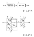
- Fig. 17A shows an arrangement using a Schmitt trigger circuit, as an example of implementation of a conventional waveform shaping circuit.
- this waveform shaping circuit shows a circuit configuration designed by taking account of a case in which an input signal IN changes from Low (a ground potential GND) to High (a power supply potential V DD ).
- this conventional waveform shaping circuit comprises a control potential setting means 11 for generating a control potential on the basis of the input signal IN, and an output means 13 for outputting an output signal OUT on the basis of the output control potential from the control potential setting means 11.
- Fig. 17B shows a practical circuit example.
- reference symbols Q1 and Q15 denote P-channel MOS transistors; Q2, Q3, Q4, and Q16, N-channel MOS transistors; and V DD ; the power supply potential.
- the control potential setting means 11 is made up of the transistors Q1, Q2, Q3, and Q4, and the output means 13 is made up of the transistors Q15 and Q16.
- These elements construct the waveform shaping circuit.
- This waveform shaping circuit outputs a signal having the same polarity as the input signal IN. If one inverter is added in series with the output means 13, the waveform shaping circuit outputs an inverted signal of the input signal IN.
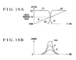
- Fig. 18A is a voltage waveform chart showing the operation of the waveform shaping circuit shown in Fig. 17B.
- the output signal changes to High when the input signal IN exceeds a logical threshold value Vth.
- the gate potential (the potential of N1 in Fig. 17B) of the transistor Q4 lowers, so the transistor Q4 is cut off. Consequently, the logical threshold value Vth of the waveform shaping circuit slightly lowers, so High can be stably output as the output potential even if the input signal IN fluctuates by the influence of external noise or the like.
- the waveform shaping circuit shown in Fig. 17B has a function of stably shaping the waveform of the input signal IN into a Low or High digital signal on the basis of the logical threshold value Vth as a boundary.
- a second arrangement in which the power supply voltage V DD and ground GND are switched by switching the polarities of the MOS transistors in the arrangement (called a first arrangement) shown in Fig. 17B.
- a circuit configuration obtained by combining the first arrangement and second arrangement is used in practice (e.g., reference [Neil H.E. Weste and another, "PRINCIPLES OF CMOS VLSI DESIGN -A Systems Perspective-", the 2nd ed., Addison-Wesley Publishing Company, 1994, p. 367]).
- the conventional waveform shaping circuit has the problem that a large through current (sink current) Itotal flows from the power supply potential V DD to the ground GND if the input signal IN is close to the logical threshold value Vth.
- the paths of the through current Itotal are: paths in which the current flows from the power supply potential V DD to the ground GND via the transistors Q1, Q2, and Q3, and via the transistors Q4 and Q3, since the transistors Q1, Q2, Q3, and Q4 are weakly turned on when the input signal IN is close to the logical threshold value Vth; and a path in which the current flows from the power supply potential V DD to the ground GND via the transistors Q15 and Q16, since the transistors Q15 and Q16 are weakly turned on when the gate potential N1 of the transistor Q4 is close to the logical threshold value Vth.
- the through current occupies a large portion of the current consumption of the overall circuit, so it is necessary to suppress the current consumption by preparing a power supply having a large current capacity, or by limiting the number of waveform shaping circuits.
- Japanese Patent Laid-Open No. 9-83345 discloses a method which performs control by a clock signal or the like by connecting a switch transistor in series in the path of the through current. This method cuts off the series-connected switch transistor when the input is at an intermediate potential and the through current flows, and turns on the switch transistor when the input signal is determined and no through current flows.
- the method disclosed in Japanese Patent Laid-Open No. 9-83345 can eliminate the through current, it cannot capture the moment at which the input signal exceeds the logical threshold value of the waveform shaping circuit. That is, the method cannot be used to detect the time at which an analog input signal having a slope exceeds the logical threshold value as disclosed in Japanese Patent No. 3082141.
- Another through current reducing method is to reduce the through current by using a dynamic operation.
- each node of the circuit is set at (charged or discharged to) a potential determined before the operation, and a switch transistor is cut off during the operation so that no through current flows.
- the charged electric charge is discharged (or the discharged electric charge is charged), and the output voltage changes.
- the waveform shaping circuit which reduces the through current by the dynamic operation has the problem that the threshold value of the circuit is the threshold voltage (normally 0.4 to 0.6 V) of a transistor. It is usually appropriate to set the logical threshold value at about half the power supply potential (e.g., 1.6 to 1.7 V when the power supply voltage is 3.3 V), but this setting cannot be performed in the waveform shaping circuit using the dynamic operation. Accordingly, no conventional method capable of setting the normal threshold value while reducing the through current by the dynamic operation has been proposed.
- the present invention provides a waveform shaping circuit which, on the basis of a logical threshold value, discriminates a level and shapes a waveform of an input signal which changes between a first power supply potential and second power supply potential, comprising first control potential setting means for generating a first control potential, second control potential setting means for generating a second control potential which changes in the same direction as the input signal in accordance with a change in input signal, output means which comprises a first transistor of a first conductivity type having a gate terminal to which the first control potential is applied, and a source terminal to which the second control potential is applied, and a second transistor of a second conductivity type having a source terminal to which the first power supply potential is applied, and a drain terminal to which the drain terminal of the first transistor is connected, and which outputs an output signal having a potential of the drain terminals of the first and second transistors, and reset means for applying a reset signal for turning off the second transistor to the gate terminal of the second transistor, wherein the first control potential setting means generates the first control potential which reverse
- the first control potential setting means comprises a third transistor of the first conductivity type having a source terminal to which the second power supply potential is applied, and a drain terminal which is connected as an output of the first control potential setting means to the gate terminal of the first transistor, a fourth transistor of the second conductivity type having a gate terminal to which the input signal is input, and a drain terminal which is connected as an output of the first control potential setting means to the gate terminal of the first transistor, a fifth transistor of the second conductivity type having a gate terminal to which the reset signal is input, a source terminal to which the first power supply potential is applied, and a drain terminal which is connected to the source terminal of the fourth transistor, an inverter gate having an input terminal to which the reset signal is input, and an output terminal which is connected to the gate terminal of the third transistor, and a first capacitance element having a first terminal which is connected to the source terminal of the fourth transistor and the drain terminal of the fifth transistor, and a second terminal to which the third power
- the first control potential setting means further comprises a second capacitance element having a first terminal which is connected to the drain terminals of the third transistor and the fourth transistor, and a second terminal to which the fourth power supply potential is applied.
- the reset means outputs the reset signal such that the second transistor is turned off before the first transistor is turned on.
- the reset means outputs the reset signal such that the second transistor is turned off before the first transistor is turned on, and the third transistor and the fifth transistor are turned off before the fourth transistor is turned on.
- the second control potential setting means sets the second control potential at the same potential as the input signal.
- the second control potential setting means comprises a signal line which shortcircuits an input terminal of the waveform shaping circuit and the source terminal of the first transistor, and sets the second control potential at the same potential as the input signal.
- the second control potential setting means comprises a sixth transistor of the second conductivity type having a gate terminal to which the input signal is applied, a drain terminal to which the second power supply potential is applied, and a source terminal which is connected to the source terminal of the first transistor, and outputs a potential of the source terminal of the sixth transistor as the second control potential.
- a configuration example of the waveform shaping circuit of the present invention further comprises third control potential setting means for compensating for the second control potential, when the input signal exceeds the logical threshold value, in accordance with the potential of the output signal.
- the third control potential setting means comprises a seventh transistor of the second conductivity type having a gate terminal to which the output signal is input, a drain terminal to which the second power supply potential is applied, and a source terminal which is connected to an input terminal or output terminal of the second control potential setting means.
- a configuration example of the waveform shaping circuit of the present invention further comprises third control potential setting means for compensating for the second control potential, when the input signal exceeds the logical threshold value, in accordance with the first control potential.
- the third control potential setting means comprises an eighth transistor of the first conductivity type having a gate terminal to which the first control potential is input, a source terminal to which the second power supply potential is applied, and a drain terminal which is connected to an input terminal or output terminal of the second control potential setting means.
- the first capacitance element is formed by a MOS capacitor.
- the first capacitance element and the second capacitance element are formed by MOS capacitors.
- the first conductivity type is a P-channel type
- the second conductivity type is an N-channel type
- the first power supply potential is a ground potential
- the second power supply potential is higher than the first power supply potential
- the first conductivity type is an N-channel type
- the second conductivity type is a P-channel type
- the first power supply potential is higher than a ground potential
- the second power supply potential is the ground potential
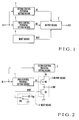
- Fig. 1 is a block diagram showing the principle of a waveform shaping circuit of the first embodiment of the present invention.
- a through current Itotal shown in Fig. 18B a through current I1 flowing through an output means reduces to zero.
- the first control potential setting means 1 comprises a first control potential setting means 1 for generating a first control potential N2, a second control potential setting means 2 for generating a second control potential N3 which changes in the same direction as an input signal IN in accordance with a change in input signal IN, an output means 3 which includes a first transistor (not shown) having a first conductivity type and a second transistor (not shown) having a second conductivity type, and generates an output signal OUT having a predetermined potential on the basis of the first control potential N2, the second control potential N3, and a reset signal RSET, and a reset means 4 for generating the reset signal RSET, and turning off the second transistor while the waveform shaping circuit is in operation.
- the first control potential setting means 1 generates the first control potential N2 which reverses the magnitude relationship with the second control potential N3, when the input signal reaches the vicinity of a logical threshold value.
- the differences from the waveform shaping circuit shown in Figs. 17A and 17B are that the second control potential setting means 2 and reset means 4 are formed, the through current I1 is reduced to zero by shutting off the through current flowing through the second transistor of the output means 3 by the reset means 4, and the logical threshold value of the waveform shaping circuit is controlled by controlling the conduction state of the first transistor of the output means 3 by using the two control potentials N2 and N3 of the first control potential setting means 1 and second control potential setting means 2, respectively.
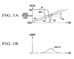
- Fig. 2 is a block diagram showing the configuration of the waveform shaping circuit of the first embodiment of the present invention.
- the output means 3 is made up of a P-channel MOS transistor Q5 as a first transistor having a gate terminal connected to the output of the first control potential setting means 1, a source terminal connected to the output of the second control potential setting means 2, and a drain terminal connected to the output terminal of the waveform shaping circuit, and an N-channel MOS transistor Q6 as a second transistor having a gate terminal connected to the output of the reset means 4, a source terminal to which a ground potential GND as a first power supply potential is applied, and a drain terminal connected to the output terminal of the waveform shaping circuit.
- the first control potential setting means 1 can have, e.g., the same arrangement as the control potential setting means 11 shown in Fig. 17B.
- the reset means 4 has a switch SW which selectively outputs a power supply potential V DD as a second power supply potential or the ground potential GND as the first power supply potential.
- a through current flowing through the N-channel MOS transistor Q6 is shut off by the reset signal RSET output from the reset means 4. If the input signal IN exceeds a logical threshold value Vth, the output signal OUT at High level can be output by turning on the P-channel MOS transistor Q5 by the first control potential setting means 1 and second control potential setting means 2.
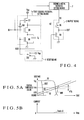
- Fig. 3A is a voltage waveform chart showing the operation of the waveform shaping circuit shown in Fig. 2.
- the reset means 4 sets the reset signal RSET at High before the waveform shaping circuit operates (when there is no signal input or when the input signal IN is fixed to the ground potential GND). Since the N-channel MOS transistor Q6 is turned on, the output signal OUT is set at Low. In this state, the first control potential setting means 1 sets the first control potential N2 at High, so the transistor Q5 is cut off.
- the reset means 4 sets the reset signal RSET at Low. As a consequence, the transistor Q6 is cut off, so no through current I1 flows from the power supply potential V DD via the transistors Q5 and Q6 of the output means 3 even if the transistor Q5 is turned on while the waveform shaping circuit is in operation. Note that the reset means 4 need only set the reset signal RSET such that when the input signal IN changes from Low to High, the transistor Q6 is turned off before the transistor Q5 is turned on.
- the first control potential N2 (the gate potential of the transistor Q5) output from the first control potential setting means 1 gradually decreases.
- the second control potential N3 the source potential of the transistor Q5 output from the second control potential setting means 2 gradually rises.
- the transistor Q5 is turned on and outputs the output signal OUT at the source potential (the potential of the input signal IN) to the output terminal of the waveform shaping circuit.
- the potential of the input signal IN is the logical threshold value Vth. After the transistor Q5 is turned on, the output signal OUT rises at the same potential as the input signal IN.
- Fig. 3B is a through current waveform chart of the waveform shaping circuit of this embodiment.
- the through current I1 can be eliminated by the dynamic operation. Accordingly, when the waveform shaping circuit of this embodiment is applied to an application which uses a number of waveform shaping circuits, it is possible to effectively reduce the through current of each waveform shaping circuit, and thereby greatly reduce the power consumption of the whole. This effect is large because it is possible to alleviate the limitations on the current capacity of the power supply device, and eliminate the limitations imposed by the power consumption on the number of waveform shaping circuits.
- this embodiment shows a circuit configuration designed by taking account of a case in which the input signal IN changes from Low (the ground potential GND) to High (the power supply potential V DD ). If the input signal IN changes from High to Low, it is only necessary, in Fig. 2, to replace the P-channel MOS transistor Q5 with an N-channel MOS transistor, and the N-channel MOS transistor Q6 with a P-channel MOS transistor, and to set the first power supply potential at the power supply potential V DD , the second power supply potential at the ground potential GND, and the reset signal RSET at Low before the waveform shaping circuit operates, and at High while the waveform shaping circuit is in operation.
- the second control potential setting means 2 can take any arbitrary arrangement, provided that it generates the second control potential N3 which changes in the same direction as the input signal IN.
- the first control potential setting means 1 can take any arbitrary arrangement, provided that it generates the first control potential N2 which reverses the magnitude relationship with the second control potential N3 when the input signal IN reaches the vicinity of the logical threshold value Vth.
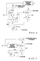
- Fig. 4 is a block diagram showing the configuration of a waveform shaping circuit of the second embodiment of the present invention.
- a through current I1 flowing through an output means 3 reduces to zero as in the first embodiment
- a through current I2 flowing through a first control potential setting means 1a also reduces to zero.
- the relationship between an input signal IN, first control potential N2, and second control potential N3 is the same as explained in the first embodiment.
- the first control potential setting means 1a comprises a P-channel MOS transistor Q7 as a third transistor having a source terminal to which a second power supply potential V DD is applied, and a drain terminal which is connected as an output of the first control potential setting means 1a to the gate terminal of a transistor Q5, an N-channel MOS transistor Q8 as a fourth transistor having a gate terminal to which the input signal IN is input, and a drain terminal which is connected as an output of the first control potential setting means 1a to the gate terminal of the transistor Q5, an N-channel MOS transistor Q9 as a fifth transistor having a gate terminal to which a reset signal RSET is input, a source terminal to which a ground potential GND is applied, and a drain terminal which is connected to the source terminal of the transistor Q8, an inverter gate INV having an input terminal to which the reset signal RSET is input, and an output terminal which is connected to the gate terminal of the transistor Q7, and a first capacitance element Cg having a first terminal which is connected to the source terminal of the
- the capacitance element Cg can be realized by a MOS capacitor, MIM (Metal-Insulator-Metal) capacitor, or PIP (Poly-Insulator-Poly) capacitor.
- the third power supply potential can be a potential at which a MOSFET of the MOS capacitor is turned on.
- the third power supply potential can be an arbitrary potential. In this embodiment, the third power supply potential is the ground potential GND.
- Fig. 5A is a voltage waveform chart showing the operation of the waveform shaping circuit shown in Fig. 4.
- a reset means 4 sets the reset signal RSET at High. Since this turns on an N-channel MOS transistor Q6, an output signal OUT is set at Low. Also, since the reset signal RSET is set at High, the P-channel transistor Q7 and N-channel transistor Q9 are turned on, so the capacitance element Cg is discharged to the ground potential GND. As a consequence, the first control potential N2 is set at High, and the transistor Q5 is cut off.
- the reset means 4 sets the reset signal RSET at Low. Since this cuts off the transistor Q6, no through current I1 flows from the power supply potential V DD via the transistors Q5 and Q6 of the output means 3, even if the transistor Q5 is turned on while the waveform shaping circuit is in operation. Similarly, the transistors Q7 and Q9 are cut off because the reset signal RSET is set at Low, so no through current I2 flows from the power supply potential V DD via the transistors Q7, Q8, and Q9 of the first control potential setting means 1a, even if the transistor Q8 is turned on while the waveform shaping circuit is in operation.
- the reset means 4 need only set the reset signal RSET such that when the input signal IN changes from Low to High, the transistor Q6 is turned off before the transistor Q5 is turned on, and the transistors Q7 and Q9 are turned off before the transistor Q8 is turned on.
- the transistor Q8 When the input signal IN gradually increases and exceeds a threshold voltage VT8 of the transistor Q8, the transistor Q8 is turned on, so the drain terminal of the transistor Q8 is connected to the capacitance element Cg. In this state, the transistors Q7 and Q9 are already cut off. Since the capacitance element Cg is connected, therefore, electric charge charged in the parasitic capacitance of the gate terminal of the transistor Q5 starts moving to the capacitance element Cg, and the first control potential N2 (the gate potential of the transistor Q5) output from the first control potential setting means 1a gradually lowers. On the other hand, the second control potential N3 (the source potential of the transistor Q5) output from the second control potential setting means 2 gradually rises.
- the transistor Q5 when the magnitude relationship between the first control potential N2 and second control potential N3 reverses and the gate-to-source voltage of the transistor Q5 exceeds a threshold voltage VT5, the transistor Q5 is turned on to output the output signal OUT at the source potential (the potential of the input signal IN) to the output terminal of the waveform shaping circuit.
- Fig. 5B is a through current waveform chart of the waveform shaping circuit of this embodiment.
- the through current I1 flowing from the power supply potential V DD via the transistor Q6 of the output means 3 can be reduced to zero.
- the first control potential setting means 1a is made up of the capacitance element Cg, the transistors Q7 and Q9 for initializing the capacitance element Cg, and the transistor Q8 for shortcircuiting the capacitance element Cg, the capacitance element Cg is initialized by turning on the transistors Q7 and Q9 by the reset means 4 before the waveform shaping circuit operates, and the output of the first control potential setting means 1a and the capacitance element Cg are connected by turning on the transistor Q8 in accordance with a change in input signal IN while the waveform shaping circuit is in operation, thereby generating the first control potential N2. Therefore, the first control potential setting means 1a can be realized without producing any through current I1 which flows via the first control potential setting means 1a. As a result, a through current Itotal is zero as shown in Fig. 5B.
- the first control potential N2 can be controlled by the capacitance element Cg, so a logical threshold value Vth of the waveform shaping circuit can be set to an appropriate value by the value of the capacitance of the capacitance element Cg.
- Fig. 6 is a block diagram showing the configuration of a waveform shaping circuit of the third embodiment of the present invention, in which the same reference numerals as in Fig. 4 denote the same parts.
- a first control potential setting means 1b of this embodiment is obtained by adding, to the first control potential setting means 1a of the second embodiment, a second capacitance element Cv having a first terminal which is connected to the drain terminals of transistors Q7 and Q8, and a second terminal to which a fourth power supply potential is applied.
- the capacitance element Cv can be realized by a MOS capacitor, MIM capacitor, or PIP capacitor.
- the fourth power supply potential can be a potential at which a MOSFET of the MOS capacitor is turned on.
- the fourth power supply potential can be an arbitrary potential.
- the fourth power supply potential can be the same as or different from the third power supply potential. In this embodiment, the fourth power supply potential is a ground potential GND.
- the operation of the waveform shaping circuit of this embodiment is substantially the same as the second embodiment.
- the differences are that the capacitance element Cv is charged to a power supply potential V DD when a reset signal RSET is at High, and that when the transistor Q8 is turned on, the capacitance elements Cv and Cg are connected, and electric charge charged in the capacitance element Cv starts moving to the capacitance element Cg, so a first control potential N2 gradually lowers.
- the first control potential N2 can be controlled by the capacitance elements Cg and Cv.
- the first control potential N2 is determined by the value of the capacitance of the capacitance element Cg, so if this value of the capacitance element Cg varies due to the process, the logical threshold value Vth of the waveform shaping circuit also varies by the influence of this variation.
- the first control potential N2 is determined by the ratio of the capacitances of the capacitance elements Cg and Cv, so the logical threshold value Vth can be stably controlled without being influenced by the process variation. This embodiment is unaffected by the process variation because even if the individual capacitances of the capacitance elements Cg and Cv vary due to the process, the ratio of the capacitances of the capacitance elements Cg and Cv does not change.
- the second and third embodiments show circuit configurations designed by taking account of a case in which the input signal IN changes from Low to High.
- the input signal IN changes from High to Low it is only necessary, in Figs. 4 and 6, to replace the P-channel MOS transistors Q5 and Q7 with N-channel MOS transistors, and the N-channel MOS transistors Q6, Q8, and Q9 with P-channel MOS transistors, and to set the first power supply potential at the power supply potential V DD , the second power supply potential at the ground potential GND, and the reset signal RSET at Low before the waveform shaping circuit operates, and at High while the waveform shaping circuit is in operation.
- Fig. 7 is a block diagram showing the configuration of a waveform shaping circuit of the fourth embodiment of the present invention, in which the same reference numerals as in Fig. 2 denote the same parts.
- This embodiment shows an example of a second control potential setting means 2.
- the second control potential setting means 2 has a signal line W which shortcircuits the input terminal of the waveform shaping circuit and the source terminal of a transistor Q5. This allows an input signal IN to have the same potential as a second control potential N3.
- the second control potential setting means 2 can be realized without increasing the number of elements, and without producing any through current which flows via the second control potential setting means 2.
- Fig. 8 is a block diagram showing the configuration of a waveform shaping circuit of the fifth embodiment of the present invention, in which the same reference numerals as in Fig. 2 denote the same parts.
- This embodiment shows another example of a second control potential setting means 2.
- the second control potential setting means 2 has an N-channel MOS transistor Q10 as a sixth transistor having a gate terminal to which an input signal IN is applied, a drain terminal to which a power supply potential V DD is applied, and a source terminal which is connected to the source terminal of a transistor Q5.
- a second control potential N3 output from the source terminal of the transistor Q10 changes in the same direction as the input signal IN in accordance with a change in input signal IN as in the first embodiment, but the magnitude of the second control potential N3 is lower than the potential of the input signal IN by the amount of threshold voltage of the transistor Q10.
- the rest of the operation is the same as in the first embodiment, so a through current can be reduced to zero as in the first embodiment.
- the output impedance of the waveform shaping circuit is affected by the input of the waveform shaping circuit. In this embodiment, however, the output impedance can be reduced by the source follower operation of the transistor Q10.
- the second control potential setting means 2 shown in Fig. 7 or 8 is applied to the first embodiment.
- the second control potential setting means 2 shown in Fig. 7 or 8 is also applicable to the second or third embodiment.
- a through current I2 flowing through a first control potential setting means 1a can also be reduced to zero, so the power consumption can be further reduced.
- the fourth and fifth embodiments show circuit configurations designed by taking account of a case in which the input signal IN changes from Low to High.
- the input signal IN changes from High to Low it is only necessary, in Figs. 7 and 8, to replace the P-channel MOS transistor Q5 with an N-channel MOS transistor, and the N-channel MOS transistors Q6 and Q10 with P-channel MOS transistors, and to set the first power supply potential at the power supply potential V DD , the second power supply potential at a ground potential GND, and a reset signal RSET at Low before the waveform shaping circuit operates, and at High while the waveform shaping circuit is in operation.
- Fig. 9 is a block diagram showing the principle of a waveform shaping circuit of the sixth embodiment of the present invention, in which the same reference numerals as in Fig. 2 denote the same parts.
- a first control potential setting means 1, second control potential setting means 2, output means 3, and reset means 4 are the same as in the first embodiment.
- the difference of this embodiment from the first embodiment is that this embodiment has a third control potential setting means 5 for compensating for a second control potential N3 of the second control potential setting means 2 in accordance with the potential of an output signal OUT.
- the use of the third control potential setting means 5 makes it possible to feed the potential of the output signal OUT back to the second control potential setting means 2 via the third control potential setting means 5, and makes the change in output signal OUT sharp when an input signal IN exceeds a logical threshold value Vth.
- the third control potential setting means 5 has an N-channel MOS transistor Q11 as a seventh transistor having a gate terminal connected to the output terminal of the waveform shaping circuit, a drain terminal to which a power supply potential V DD is applied, and a source terminal connected to the input terminal or output terminal of the second control potential setting means 2.
- Fig. 11A is a voltage waveform chart showing the operation of the waveform shaping circuit.
- the operation before the input signal IN exceeds the logical threshold value Vth is the same as in the first embodiment.
- a transistor Q5 is turned on, and the output signal OUT changes from Low to High, so the transistor Q11 is turned on.
- the input signal IN abruptly rises toward the power supply potential V DD , so the second control potential N3 which is the same as the power supply potential V DD also abruptly rises. Consequently, as shown in Fig. 11A, the output signal OUT abruptly rises.
- the input signal IN rises to a level lower than the power supply potential V DD by the amount of threshold voltage VT11 of the transistor Q11, the transistor Q11 is cut off, and the potential of the input signal IN moderately rises in accordance with the original change in input signal itself.
- Fig. 11B is a through current waveform chart of the waveform shaping circuit of this embodiment.
- a through current I1 which flows from the power supply potential V DD via a transistor Q6 of an output means 3 can be reduced to zero.
- the use of the third control potential setting means 5 makes it possible to compensate for the level of the output signal OUT when the input signal IN exceeds the logical threshold value Vth.
- Fig. 12 is a block diagram showing the configuration of a waveform shaping circuit of the seventh embodiment of the present invention, in which the same reference numerals as in Fig. 10 denote the same parts.
- the arrangement of the fourth embodiment shown in Fig. 7 is used as the arrangement of the second control potential setting means 2.
- the arrangement of the fifth embodiment shown in Fig. 8 is used as the arrangement of a second control potential setting means 2.
- the source terminal of a transistor Q11 is connected to the input terminal (the gate terminal of a transistor Q10) or the output terminal (the source terminals of a transistor Q5 and the transistor Q10) of the second control potential setting means 2. Therefore, the source terminal of the transistor Q11 may also be connected to the source terminals of the transistors Q5 and Q10.
- Fig. 13 is a block diagram showing the principle of a waveform shaping circuit of the eighth embodiment of the present invention, in which the same reference numerals as in Fig. 2 denote the same parts.
- a first control potential setting means 1, second control potential setting means 2, output means 3, and reset means 4 are the same as in the first embodiment.
- the difference of this embodiment from the first embodiment is that this embodiment has a third control potential setting means 5a for compensating for a second control potential N3 of the second control potential setting means 2 in accordance with the potential of a first control potential N2.
- the use of the third control potential setting means 5a makes it possible to feed the first control potential N2 back to the second control potential setting means 2 via the third control potential setting means 5a, and makes the change in output signal OUT sharp when an input signal IN exceeds a logical threshold value Vth.
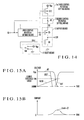
- the third control potential setting means 5a has an P-channel MOS transistor Q12 as an eighth transistor having a gate terminal to which the first control potential N2 is input, a source terminal to which a power supply potential V DD is applied, and a drain terminal connected to the input terminal or output terminal of the second control potential setting means 2.
- Fig. 15A is a voltage waveform chart showing the operation of the waveform shaping circuit.
- the operation before the input signal IN exceeds the logical threshold value Vth is the same as in the first embodiment.
- the first control potential N2 gradually lowers in accordance with the rise of the input signal IN, and, when the input signal IN exceeds the logical threshold value Vth and the magnitude relationship between the first control potential N2 and second control potential N3 reverses, the transistor Q12 is turned on.
- the input signal IN abruptly rises toward the power supply potential V DD , so the second control potential N3 which is the same as the power supply potential V DD also abruptly rises. Consequently, as shown in Fig. 15A, the output signal OUT abruptly rises.
- the transistor Q11 when the input signal IN exceeds the logical threshold value Vth, the transistor Q11 is once turned on and then cut off again, so the output signal OUT moderates its change before reaching the power supply potential V DD .
- the transistor Q12 is not cut off again while the input signal IN exceeds the logical threshold value Vth. This can make the change in output signal OUT sharper than in the sixth and seventh embodiments.
- Fig. 15B is a through current waveform chart of the waveform shaping circuit of this embodiment.
- a through current I1 which flows from the power supply potential V DD via a transistor Q6 of an output means 3 can be reduced to zero.
- the use of the third control potential setting means 5a makes it possible to compensate for the level of the output signal OUT when the input signal IN exceeds the logical threshold value Vth.
- Fig. 16 is a block diagram showing the configuration of a waveform shaping circuit of the ninth embodiment of the present invention, in which the same reference numerals as in Fig. 14 denote the same parts.
- the arrangement of the fourth embodiment shown in Fig. 7 is used as the arrangement of the second control potential setting means 2.
- the arrangement of the fifth embodiment shown in Fig. 8 is used as the arrangement of a second control potential setting means 2. In this manner, the same effects as in the eighth embodiment can be obtained in this embodiment.
- the drain terminal of a transistor Q12 is connected to the input terminal or output terminal of the second control potential setting means 2, so the drain terminal of the transistor Q12 may also be connected to the source terminals of transistors Q5 and Q10.
- the third control potential setting means 5 shown in Fig. 10 or 12 or the third control potential setting means 5a shown in Fig. 14 or 16 is applied to the first embodiment.
- the third control potential setting means 5 or 5a is also applicable to the second or third embodiment.
- the sixth to ninth embodiments show circuit configurations designed by taking account of a case in which the input signal IN changes from Low to High.
- the input signal IN changes from High to Low it is only necessary, in Figs. 10, 12, 14 and 16, to replace the P-channel MOS transistors Q5 and Q12 with N-channel MOS transistors, and the N-channel MOS transistors Q6, Q10, and Q11 with P-channel MOS transistors, and to set the first power supply potential at the power supply potential V DD , the second power supply potential at the ground potential GND, and the reset signal RSET at Low before the waveform shaping circuit operates, and at High while the waveform shaping circuit is in operation.
- the output signal OUT having the same polarity as the input signal IN is output.
- the waveform shaping circuit when an inverter is added after the output means 3, the waveform shaping circuit, of course, outputs an inverted signal of the input signal IN.
- the reset means 4 is controlled by a control means (not shown).
- This control means controls the reset means 4 to output the reset signal RSET under the above-mentioned conditions, in accordance with the timing at which the input signal IN is input from a gate circuit (not shown) or the like to the waveform shaping circuit.
- the control means can also control the reset means 4 to output the reset signal RSET under the above-mentioned conditions, by observing the level of the input signal IN (or observing the levels of the first control potential N2 and second control potential N3 in addition to the input signal IN).
- the waveform shaping circuit of the present invention is useful in an apparatus required to reduce the power consumption, and is suitably incorporated into a battery-driven portable terminal apparatus.
Landscapes
- Physics & Mathematics (AREA)
- Nonlinear Science (AREA)
- Logic Circuits (AREA)
- Manipulation Of Pulses (AREA)
- Electronic Switches (AREA)
Applications Claiming Priority (2)
| Application Number | Priority Date | Filing Date | Title |
|---|---|---|---|
| JP2003014834 | 2003-01-23 | ||
| PCT/JP2004/000506 WO2004066500A1 (ja) | 2003-01-23 | 2004-01-21 | 波形整形回路 |
Publications (3)
| Publication Number | Publication Date |
|---|---|
| EP1633048A1 true EP1633048A1 (de) | 2006-03-08 |
| EP1633048A4 EP1633048A4 (de) | 2006-04-05 |
| EP1633048B1 EP1633048B1 (de) | 2012-10-10 |
Family
ID=32767419
Family Applications (1)
| Application Number | Title | Priority Date | Filing Date |
|---|---|---|---|
| EP04703946A Expired - Lifetime EP1633048B1 (de) | 2003-01-23 | 2004-01-21 | Schaltungen zur signalformung |
Country Status (5)
| Country | Link |
|---|---|
| US (1) | US7019563B2 (de) |
| EP (1) | EP1633048B1 (de) |
| JP (1) | JP3899110B2 (de) |
| CN (1) | CN100355209C (de) |
| WO (1) | WO2004066500A1 (de) |
Families Citing this family (2)
| Publication number | Priority date | Publication date | Assignee | Title |
|---|---|---|---|---|
| CN103248343B (zh) * | 2012-02-10 | 2016-03-30 | 国际商业机器公司 | 用于校正时钟占空比的边沿选择技术 |
| CN103297001B (zh) * | 2013-05-17 | 2016-06-22 | 中科院微电子研究所昆山分所 | 一种脉冲整形电路及脉冲整形方法 |
Family Cites Families (8)
| Publication number | Priority date | Publication date | Assignee | Title |
|---|---|---|---|---|
| JPS58151124A (ja) | 1982-03-04 | 1983-09-08 | Ricoh Co Ltd | レベル変換回路 |
| JP3618424B2 (ja) | 1995-09-07 | 2005-02-09 | エイ・アイ・エル株式会社 | 低消費電力論理回路 |
| JPH09116422A (ja) | 1995-10-23 | 1997-05-02 | Hitachi Ltd | 半導体論理回路 |
| JP3082141B1 (ja) * | 1999-06-04 | 2000-08-28 | 日本電信電話株式会社 | 表面形状認識用センサ回路 |
| EP0969477B1 (de) * | 1998-07-02 | 2006-09-27 | Nippon Telegraph and Telephone Corporation | Nachweisvorrichtung für kleine Kapazitätsänderungen |
| JP3482141B2 (ja) | 1998-10-06 | 2003-12-22 | 株式会社愛徳 | 船舶の推進操向装置 |
| JP3829054B2 (ja) * | 1999-12-10 | 2006-10-04 | 株式会社東芝 | 半導体集積回路 |
| US6646469B2 (en) * | 2001-12-11 | 2003-11-11 | Koninklijke Philips Electronics N.V. | High voltage level shifter via capacitors |
-
2004
- 2004-01-21 US US10/505,629 patent/US7019563B2/en not_active Expired - Fee Related
- 2004-01-21 JP JP2005507684A patent/JP3899110B2/ja not_active Expired - Lifetime
- 2004-01-21 EP EP04703946A patent/EP1633048B1/de not_active Expired - Lifetime
- 2004-01-21 WO PCT/JP2004/000506 patent/WO2004066500A1/ja not_active Ceased
- 2004-01-21 CN CNB2004800000468A patent/CN100355209C/zh not_active Expired - Fee Related
Also Published As
| Publication number | Publication date |
|---|---|
| US7019563B2 (en) | 2006-03-28 |
| JP3899110B2 (ja) | 2007-03-28 |
| CN1698269A (zh) | 2005-11-16 |
| JPWO2004066500A1 (ja) | 2006-05-18 |
| EP1633048B1 (de) | 2012-10-10 |
| WO2004066500A1 (ja) | 2004-08-05 |
| US20050258877A1 (en) | 2005-11-24 |
| EP1633048A4 (de) | 2006-04-05 |
| CN100355209C (zh) | 2007-12-12 |
Similar Documents
| Publication | Publication Date | Title |
|---|---|---|
| KR101293845B1 (ko) | 지연 회로 | |
| US7986172B2 (en) | Switching circuit with gate driver having precharge period and method therefor | |
| JPH0584597B2 (de) | ||
| US8269547B2 (en) | Bootstrap circuit | |
| EP0675601B1 (de) | Schaltung zur Verbesserung der auf einer Leitung auftretenden Logiksignalübergänge | |
| US10270363B2 (en) | CMOS inverter circuit that suppresses leakage currents | |
| US5151620A (en) | CMOS input buffer with low power consumption | |
| US6677798B2 (en) | High speed voltage level shifter | |
| JPH0158896B2 (de) | ||
| JP3949027B2 (ja) | アナログスイッチ回路 | |
| US20160149576A1 (en) | Low voltage differential signaling (lvds) driving circuit | |
| JPH10224191A (ja) | 遅延回路 | |
| US6980194B2 (en) | Amplitude conversion circuit for converting signal amplitude | |
| JPH08294267A (ja) | 昇圧回路 | |
| US8466722B2 (en) | Startup and protection circuitry for thin oxide output stage | |
| JP4229804B2 (ja) | 半導体出力回路 | |
| US20040041614A1 (en) | Amplitude converting circuit | |
| US6982577B2 (en) | Power-on reset circuit | |
| EP1633048B1 (de) | Schaltungen zur signalformung | |
| US20030169224A1 (en) | Amplitude conversion circuit for converting signal amplitude and semiconductor device using the amplitude conversion circuit | |
| US9172374B2 (en) | Voltage level translator | |
| JP2001044819A (ja) | 高電圧出力インバーター | |
| JP2015136003A (ja) | パワーオンリセット回路 | |
| KR960015319B1 (ko) | 반도체 메모리 장치의 전압 변환회로 | |
| JP3083654B2 (ja) | 出力回路 |
Legal Events
| Date | Code | Title | Description |
|---|---|---|---|
| PUAI | Public reference made under article 153(3) epc to a published international application that has entered the european phase |
Free format text: ORIGINAL CODE: 0009012 |
|
| 17P | Request for examination filed |
Effective date: 20040902 |
|
| AK | Designated contracting states |
Kind code of ref document: A1 Designated state(s): DE FR GB |
|
| A4 | Supplementary search report drawn up and despatched |
Effective date: 20060220 |
|
| DAX | Request for extension of the european patent (deleted) | ||
| RBV | Designated contracting states (corrected) |
Designated state(s): DE FR GB |
|
| 17Q | First examination report despatched |
Effective date: 20101025 |
|
| GRAP | Despatch of communication of intention to grant a patent |
Free format text: ORIGINAL CODE: EPIDOSNIGR1 |
|
| GRAC | Information related to communication of intention to grant a patent modified |
Free format text: ORIGINAL CODE: EPIDOSCIGR1 |
|
| GRAC | Information related to communication of intention to grant a patent modified |
Free format text: ORIGINAL CODE: EPIDOSCIGR1 |
|
| GRAS | Grant fee paid |
Free format text: ORIGINAL CODE: EPIDOSNIGR3 |
|
| GRAA | (expected) grant |
Free format text: ORIGINAL CODE: 0009210 |
|
| AK | Designated contracting states |
Kind code of ref document: B1 Designated state(s): DE FR GB |
|
| REG | Reference to a national code |
Ref country code: GB Ref legal event code: FG4D |
|
| REG | Reference to a national code |
Ref country code: DE Ref legal event code: R096 Ref document number: 602004039605 Country of ref document: DE Effective date: 20121206 |
|
| PLBE | No opposition filed within time limit |
Free format text: ORIGINAL CODE: 0009261 |
|
| STAA | Information on the status of an ep patent application or granted ep patent |
Free format text: STATUS: NO OPPOSITION FILED WITHIN TIME LIMIT |
|
| 26N | No opposition filed |
Effective date: 20130711 |
|
| REG | Reference to a national code |
Ref country code: DE Ref legal event code: R097 Ref document number: 602004039605 Country of ref document: DE Effective date: 20130711 |
|
| REG | Reference to a national code |
Ref country code: FR Ref legal event code: PLFP Year of fee payment: 12 |
|
| PGFP | Annual fee paid to national office [announced via postgrant information from national office to epo] |
Ref country code: GB Payment date: 20141126 Year of fee payment: 12 |
|
| PGFP | Annual fee paid to national office [announced via postgrant information from national office to epo] |
Ref country code: FR Payment date: 20150128 Year of fee payment: 12 |
|
| PGFP | Annual fee paid to national office [announced via postgrant information from national office to epo] |
Ref country code: DE Payment date: 20150327 Year of fee payment: 12 |
|
| REG | Reference to a national code |
Ref country code: DE Ref legal event code: R119 Ref document number: 602004039605 Country of ref document: DE |
|
| GBPC | Gb: european patent ceased through non-payment of renewal fee |
Effective date: 20160121 |
|
| REG | Reference to a national code |
Ref country code: FR Ref legal event code: ST Effective date: 20160930 |
|
| PG25 | Lapsed in a contracting state [announced via postgrant information from national office to epo] |
Ref country code: GB Free format text: LAPSE BECAUSE OF NON-PAYMENT OF DUE FEES Effective date: 20160121 Ref country code: DE Free format text: LAPSE BECAUSE OF NON-PAYMENT OF DUE FEES Effective date: 20160802 |
|
| PG25 | Lapsed in a contracting state [announced via postgrant information from national office to epo] |
Ref country code: FR Free format text: LAPSE BECAUSE OF NON-PAYMENT OF DUE FEES Effective date: 20160201 |