EP1628224A2 - Method for controlling memories of a plurality of kinds and circuit for controlling memories of a plurality of kinds - Google Patents
Method for controlling memories of a plurality of kinds and circuit for controlling memories of a plurality of kinds Download PDFInfo
- Publication number
- EP1628224A2 EP1628224A2 EP05018000A EP05018000A EP1628224A2 EP 1628224 A2 EP1628224 A2 EP 1628224A2 EP 05018000 A EP05018000 A EP 05018000A EP 05018000 A EP05018000 A EP 05018000A EP 1628224 A2 EP1628224 A2 EP 1628224A2
- Authority
- EP
- European Patent Office
- Prior art keywords
- control circuit
- memory
- memory access
- memories
- instruction
- Prior art date
- Legal status (The legal status is an assumption and is not a legal conclusion. Google has not performed a legal analysis and makes no representation as to the accuracy of the status listed.)
- Withdrawn
Links
Images





Classifications
-
- G—PHYSICS
- G11—INFORMATION STORAGE
- G11C—STATIC STORES
- G11C11/00—Digital stores characterised by the use of particular electric or magnetic storage elements; Storage elements therefor
- G11C11/21—Digital stores characterised by the use of particular electric or magnetic storage elements; Storage elements therefor using electric elements
- G11C11/34—Digital stores characterised by the use of particular electric or magnetic storage elements; Storage elements therefor using electric elements using semiconductor devices
- G11C11/40—Digital stores characterised by the use of particular electric or magnetic storage elements; Storage elements therefor using electric elements using semiconductor devices using transistors
- G11C11/401—Digital stores characterised by the use of particular electric or magnetic storage elements; Storage elements therefor using electric elements using semiconductor devices using transistors forming cells needing refreshing or charge regeneration, i.e. dynamic cells
- G11C11/4063—Auxiliary circuits, e.g. for addressing, decoding, driving, writing, sensing or timing
- G11C11/407—Auxiliary circuits, e.g. for addressing, decoding, driving, writing, sensing or timing for memory cells of the field-effect type
- G11C11/409—Read-write [R-W] circuits
- G11C11/4093—Input/output [I/O] data interface arrangements, e.g. data buffers
-
- G—PHYSICS
- G06—COMPUTING OR CALCULATING; COUNTING
- G06F—ELECTRIC DIGITAL DATA PROCESSING
- G06F13/00—Interconnection of, or transfer of information or other signals between, memories, input/output devices or central processing units
- G06F13/14—Handling requests for interconnection or transfer
- G06F13/16—Handling requests for interconnection or transfer for access to memory bus
- G06F13/1668—Details of memory controller
- G06F13/1694—Configuration of memory controller to different memory types
-
- G—PHYSICS
- G11—INFORMATION STORAGE
- G11C—STATIC STORES
- G11C11/00—Digital stores characterised by the use of particular electric or magnetic storage elements; Storage elements therefor
- G11C11/21—Digital stores characterised by the use of particular electric or magnetic storage elements; Storage elements therefor using electric elements
- G11C11/34—Digital stores characterised by the use of particular electric or magnetic storage elements; Storage elements therefor using electric elements using semiconductor devices
- G11C11/40—Digital stores characterised by the use of particular electric or magnetic storage elements; Storage elements therefor using electric elements using semiconductor devices using transistors
- G11C11/401—Digital stores characterised by the use of particular electric or magnetic storage elements; Storage elements therefor using electric elements using semiconductor devices using transistors forming cells needing refreshing or charge regeneration, i.e. dynamic cells
- G11C11/4063—Auxiliary circuits, e.g. for addressing, decoding, driving, writing, sensing or timing
- G11C11/407—Auxiliary circuits, e.g. for addressing, decoding, driving, writing, sensing or timing for memory cells of the field-effect type
- G11C11/4076—Timing circuits
-
- G—PHYSICS
- G11—INFORMATION STORAGE
- G11C—STATIC STORES
- G11C7/00—Arrangements for writing information into, or reading information out from, a digital store
- G11C7/22—Read-write [R-W] timing or clocking circuits; Read-write [R-W] control signal generators or management
Definitions
- the present invention relates to a method for controlling memories such as DRAMs and its memory control circuit.
- the present invention relates to a technique for making it possible to control memories of a plurality of kinds differing in control system by using the same controller (memory control circuit).
- DRAM dynamic random access memory
- SDRAM synchronous DRAM
- the DDR (double data rate) - SDRAM based on the SDRAM which conducts data transfer not only at timing of a rising edge of the clock but also at timing of a falling edge has become the main stream (see, for example, JP-A-2000-173267).
- DDR-SDRAM is also being gradually replaced by DDR2-SDRAM which is an improved version of the DDR-SDRAM.
- FC (fast cycle) - DRAM which takes in a row address and a column address simultaneously (at consecutive clocks) is also proposed and provided for the market (see, for example, WO98/56004).
- the memory such as the DRAM executes an instruction issued by a high rank control unit such as a CPU via an LSI called controller.
- controllers must be developed respectively for different kinds of DRAMs in the same application device.
- the total time and labor required for the development is increased.
- design and development of the controllers must be started after the specifications of the DRAMs have been completely fixed. In situations where the development cycles of application devices become short, like the present, therefore, a fear that the development will be delayed occurs.
- a first object of the present invention is to make it possible to cope with memories of a plurality of kinds differing in control system by using a single controller and shorten the total time and labor required for the development of the controller.
- a second object of the present invention is to make it possible to develop an application device in parallel with development of a memory to be mounted on the application device and cope with shortening of the development cycle of the application device.
- a third object is to make it possible to flexibly cope with an alteration in memory specifications without re-developing the controller (LSI).
- the present invention provides a method for controlling memories of a plurality of kinds by supplying control signals to the memories and exercising data input and output control, the method including the steps of storing various instructions to be supplied to memories of a plurality of kinds differing in control system, in a memory access common control circuit for supplying control signals to the memories, and successively selecting and outputting the instructions stored in the memory access common control circuit in accordance with an output signal of a memory access management circuit for managing memory access timing.
- the present invention provides a memory control circuit for controlling memories of a plurality of kinds by supplying control signals to the memories and exercising data input and output control, the memory control circuit including a memory access management circuit for managing memory access timing, and a memory access common control circuit for supplying control signals to the memories, wherein various instructions to be supplied to memories of a plurality of kinds differing in control system are stored in the memory access common control circuit, and the instructions stored in the memory access common control circuit are successively selected and output in accordance with an output signal of the memory access management circuit.
- the instruction stored in the memory access common control circuit can be set by software.
- the present invention makes it possible to implement an LSI (controller) for memory control by using a single LSI kind, reduce the total time and labor required for the development, and eventually reduce the development cost.
- FIG. 1 is a block diagram showing a configuration of a memory control circuit according to the present invention.
- a memory control circuit 1 includes a memory access RAM busy management circuit 11, a RAM classification register 12, and a memory access common control circuit 13.
- the memory control circuit 1 is constituted as an LSI.
- the memory control circuit 1 receives a RAM access request signal 100, which does not depend on the classification of a RAM device, from a high rank control unit (not illustrated) such as a CPU, and transmits a RAM control signal & data group 200 to a subordinate RAM device 10 to control it.
- the RAM access request signal 100 is received by the memory access RAM busy management circuit 11.
- the memory access RAM busy management circuit 11 refers to a RAM classification signal 400 transmitted from the RAM classification register 12, generates RAM control command & data 300 suitable for the currently connected RAM device 10, and transmits the RAM control command & data 300 to the memory access common control circuit 13.
- the memory access common control circuit 13 Upon receiving the RAM control command & data 300, the memory access common control circuit 13 generates RAM control signal & data group 200, and transmits the RAM control signal & data group 200 to the RAM device 10.
- the memory access RAM busy management circuit 11 to which the RAM access request signal 100 is transmitted from the high rank control unit is a circuit typically used in the conventional controller.
- the memory access RAM busy management circuit 11 receives the RAM classification signal 400 from the RAM classification register 12, which manages the classification of the RAM device connected to the memory control circuit 1, and exercises control (busy control) on a timing interval of sending a control signal to the RAM according to specifications of the RAM device.
- the memory access RAM busy management circuit 11 sends the RAM control command & data 300 to the memory access common control circuit 13.
- the memory access common control circuit 13 transmits the RAM control signal & data group 200, which contains a control signal, data and address information, to the RAM device 10.
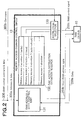
- FIG. 2 is a block diagram showing a detailed configuration of the memory access control circuit 13 shown in FIG. 1.
- the memory access common control circuit 13 receives information required for RAM access [such as the RAM access kind (such as writing, reading or refreshing), an access address in the RAM, and data] as the RAM control command & data 300 sent from the memory access RAM busy management circuit 11 shown in FIG. 1, conducts generation of an interface signal between the RAM device 10 and the memory control circuit 1, and exercises timing control.
- the memory access common control circuit 13 includes a RAM address & data control unit 131, a RAM access instruction definition register 132, and an instruction selector 133.
- the RAM address & data control unit 131 is supplied with address data 300a from among the RAM control command & data 300 sent from the memory access RAM busy management circuit 11. And an inter-RAM address signal 200b and write data are transmitted from the RAM address & data control unit 131 to the RAM device 10.
- Read data from the RAM device 10 is sent to the RAM address & data control unit 131.
- Instructions (commands) required to control RAM devices differing in control system are previously registered in the RAM access instruction definition register 132.
- instructions associated with respective RAMs including a write instruction, a full write instruction, a mask write instruction, a refresh instruction (REF) and a mode register set (MRS) instruction are previously registered in the RAM access instruction definition register 132.
- a command 300b in the RAM control command & data 300 sent from the memory access RAM busy management circuit 11 is sent to the instruction selector 133.
- the instruction selector 133 selects an instruction registered in the RAM access instruction definition register 132 on the basis of the command 300b, at its sending timing, and outputs the selected instruction toward the RAM device 10 as a RAM control signal 200c.
- the instruction selector 133 outputs instructions registered in the RAM access instruction definition register 132 toward the RAM device 10 one after another.
- the output timing is controlled by the memory access RAM busy management circuit 11.
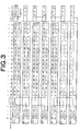
- FIG. 3 is a diagram showing pin names and their signal assignments in the FCRAM controlled by the memory control circuit in an example of the present invention.
- pins CLK, CLK', CS', WE', CKE, BA0, BA1, A0 to A14, DQS, DQS', and DQ0 to DQ7 are used.
- Clocks CLK and CLK' are input to the CLK pin and the CLK' pin, respectively.
- a CS' signal is input to the CS' pin.
- An FN signal is input to the WE' pin.
- a power down command PD' is input to the CKE pin.
- the power down command is not originated and consequently the CKE pin is fixed to a high level.
- Bank addresses BA0 and BA1 are input to the BA0 pin and the BA1 pin, respectively.
- Upper addresses UA00 to UA14 are respectively input to the A0 to A14 pins at the time of a 1st command.
- lower addresses LA00 to LA08 are respectively input to the A0 to A8 pins and variable write signals VW1 and VW0 are respectively input to the A13 pin and A14 pin.
- VW1 and VW0 are input only at the time of write command origination.
- Data strobe signals DQS and DQS' are input to and output from the DQS pin and DQS' pin, respectively.
- Data DQ0 to DQ7 are input to and output from the DQ0 to DQ7 pins, respectively.
- the CS' signal goes “L” and the FN signal goes “H” at the time of 1st command and consequently an RDA (read with auto-close) command is issued.
- the band addresses BA0 and BA1 are taken in respectively from the BA0 pin and the BA1 pin, and upper addresses A(00) to A(14) are taken in respectively from the A0 pin to A14 pin.
- the CS' signal goes “H” and the FN signal goes “H” and consequently a LAL (lower address latch) command is issued.
- lower addresses A(15) to A(21) are taken in from the A2 pin to A8 pin, respectively.
- information stored in a cell of a specific address is read out via DQ0 to DQ7 pins.
- Commands used when conducting upper writing or lower writing, which is mask writing, on the FCRAM are the same as those used at the time of full writing except that information "H” and "L” indicating the mask writing is supplied to the A13 pin and the A14 pin at the time of the 2nd command.
- the mask place for the upper write or the lower write are indicated via the A0 pin and the A1 pin at the time of 2nd command.
- the CS' signal When conducting refreshing on the FCRAM, the CS' signal goes “L” and the FN signal goes “L” at the time of the 1st command and consequently the WRA command is issued. At the time of the 2nd command, the CS' signal goes “L” and the FN signal goes “H” and consequently an REF (auto refresh) command is issued and refreshing is conducted.
- REF auto refresh
- the CS' signal goes “L” and the FN signal goes “H” at the time of the 1st command and consequently the RDA command is issued.
- the CS' signal goes “L” and the FN signal goes “H” and consequently a MRS (mode register set) command is issued.
- information concerning the mode to be set is supplied from address pins.
- the DQS, DQS' and DQ0 to DQ7 pins are placed in the high impedance state.
- FIG. 4 is a diagram showing pin names and their signal assignments in the DDR2-SDRAM controlled by the memory control circuit in the example of the present invention.
- pins CLK, CLK', CS', RAS', CAS', WE', CKE, BA0, BA1, A0 to A13, DM, DQS, DQS', and DQ0 to DQ7 are used.
- the clocks CLK and CLK' are input to the CLK pin and the CLK' pin, respectively.
- a CS' signal is input to the CS' pin.
- An RAS' signal and a CAS' signal are input to the RAS' pin and the CAS' pin.
- a WE' signal is input to the WE' pin.
- a clock enable signal CKE fixed to the high level in the present example is input to the CKE pin.
- Bank addresses BA0 and BA1 are input to the BA0 pin and the BA1 pin, respectively.
- Row addresses RA00 to RA13 are respectively input to the A0 to A13 pins at the time of a 1st command.
- column addresses CA00 to CA09 are respectively input to the A0 to A9 pins and an auto precharge signal AP is input to the A10 pin.
- a data mask signal DM is input to the DM pin.
- Data strobe signals DQS and DQS' are input to and output from the DQS pin and DQS' pin, respectively.
- Data DQ0 to DQ7 are input to and output from the DQ0 to DQ7 pins, respectively.
- the CS' signal goes “L” and the RAS signal goes “H” at the time of 1st command and consequently an ACT (active) command is issued.
- the band addresses BA0 and BA1 are taken in respectively from the BA0 pin and the BA1 pin
- row addresses A(00) to A(13) are taken in respectively from the A0 pin to A13 pin.
- the CS' signal, the CAS' signal and the AP signal respectively go “L”, “L” and “H” and consequently the RDA (read with auto precharge) command is issued.
- column addresses A(14) to A(21) are taken in from the A2 pin to A9 pin, respectively. As a result, information stored in a cell of a specific address is read out via DQ0 to DQ7 pins.
- the CS' signal, the RAS' signal and the CAS' signal respectively go “L”, “L” and 1"L” and consequently the REF command is issued. After completion of refreshing, a return to the standby state is conducted.
- the CS' signal, the RAS' signal, the CAS' signal, and the WE' signal respectively go “L”, “L”, “L” and “L” and consequently the MRS command is issued.
- information concerning the mode to be set is supplied from the address pins.
- the DQS, DQS' and DQ0 to DQ7 pins are placed in the high impedance state.
- FIG. 5 is a time chart showing operation waveforms at respective pins at the time when writing data into the FCRAM which operates according to the signal assignment shown FIG. 3.
- BL burst length
- WL write latency
- the full write command (8BW) is input.
- the upper write command (4BWU) is input.
- the lower write command (4BWL) is input.
- both CS' and FN go "L” and the WRA command is issued.
- the bank addresses BA0 and BA1 and the upper addresses UA0 to UA14 are taken in.
- both CS' and FN go "H” and the LAL command is issued.
- the lower addresses LA2 to UA8 are taken in.
- the same operation as that in the full write 8BW is conducted except the mask writing is executed by inputting a mask write indicating signal from the A13 and A14 pins and inputting mask position indicating information from the A0 and A1 pins.
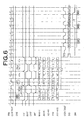
- FIG. 6 is a time chart showing operation waveforms at respective pins at the time when writing data into the DDR2-SDRAM which operates according to the signal assignment shown FIG. 4.
- BL is set equal to 4 and WL is set equal to 6.
- the full write command (8BW) is input.
- the upper write command (4BWU) is input.
- the lower write command (4BWL) is input.
- FIG. 7 is a block diagram of the memory access common control circuit installed in the memory control circuit in the present example.
- the RAM device 10 connected to a memory access common control circuit 23 is the FCRAM or the DDR2-SDRAM described with reference to FIGS. 3 to 6.
- the memory access common control circuit 23 includes a RAM address & data control unit 231, a RAM access instruction definition register 232, an instruction selector 233, and an instruction & address selector 234.
- the RAM address & data control unit 231 is supplied with address data 300a from among the RAM control command & data 300. Inputting and outputting of data 200a are conducted between the RAM address & data control unit 231 and the RAM device 10.
- the RAM address & data control unit 231 outputs an intra-RAM address signal 200b.
- Various instructions of the RAM connected to the memory control circuit in the present example i.e., various instructions of the FCRAM and the DDR2-SDRAM are stored in the RAM access instruction definition register 232.
- a read instruction (8BR), a full write instruction (8BW), an upper write instruction (4BWU), a lower write instruction (4BWL), an auto refresh instruction (REF) and a mode register set instruction (MRS) for the FCRAM and a read instruction (8BR), a full write instruction (8BW), a mask write instruction (4BWU, 4BWL), an auto refresh instruction (REF) and a mode register set instruction (MRS) for the DDR2-SDRAM are set.
- a command 300b in the RAM control command & data 300 is input to the instruction selector 233.
- the instruction selector 233 selects an instruction registered in the RAM access instruction definition register 232 in accordance with the command 300b, and outputs the selected instruction as a RAM control signal 200c.
- a part (signals at A0, A1, A10, A13 and A14 pins) of the intra-RAM address signal 200b and a part (address control signal) of the RAM control signal 200c are input to the instruction & address selector 234.
- the instruction & address selector 234 outputs either of them toward the RAM device 10 in accordance with the command 300b.
- the contents of the RAM access instruction definition register 232 may be adapted to be set by setting dip switches or programming programmable elements.
- FIG. 8 is a diagram showing a specific registration example of the RAM access instruction definition register 232 shown in FIG. 7. Registration is conducted beforehand as shown in FIG. 8 in accordance with signal assignments of respective pins shown in FIGS. 3 and 4.
Landscapes
- Engineering & Computer Science (AREA)
- Theoretical Computer Science (AREA)
- Physics & Mathematics (AREA)
- General Engineering & Computer Science (AREA)
- General Physics & Mathematics (AREA)
- Microelectronics & Electronic Packaging (AREA)
- Computer Hardware Design (AREA)
- Dram (AREA)
- Memory System (AREA)
- Communication Control (AREA)
Abstract
Description
- The present invention relates to a method for controlling memories such as DRAMs and its memory control circuit. In particular, the present invention relates to a technique for making it possible to control memories of a plurality of kinds differing in control system by using the same controller (memory control circuit).
- In the DRAM (dynamic random access memory) which is a representative memory, an SDRAM (synchronous DRAM) which conducts operation in synchronism with a clock supplied from the outside has become general. At present, however, the DDR (double data rate) - SDRAM based on the SDRAM which conducts data transfer not only at timing of a rising edge of the clock but also at timing of a falling edge has become the main stream (see, for example, JP-A-2000-173267). This DDR-SDRAM is also being gradually replaced by DDR2-SDRAM which is an improved version of the DDR-SDRAM. Furthermore, the FC (fast cycle) - DRAM which takes in a row address and a column address simultaneously (at consecutive clocks) is also proposed and provided for the market (see, for example, WO98/56004). Typically, the memory such as the DRAM executes an instruction issued by a high rank control unit such as a CPU via an LSI called controller.
- On the other hand, in an application device such as a personal computer having a DRAM mounted thereon, it is necessary to provide a device obtained by mounting DRAMs differing in control system, such as the DDR-SDRAM and the FCRAM, on a device of the same device kind in order to meet various needs of users. In such a case, it becomes necessary to develop separate controllers respectively for the DDR-SDRAM and the FCRAM differing from each other in control system.
- However, controllers must be developed respectively for different kinds of DRAMs in the same application device. When developing a device with RAMs that are different in control system mounted thereon in order to, for example, increase variations in the same device kind, therefore, the total time and labor required for the development is increased. Furthermore, in the conventional method, design and development of the controllers must be started after the specifications of the DRAMs have been completely fixed. In situations where the development cycles of application devices become short, like the present, therefore, a fear that the development will be delayed occurs. In addition, in the conventional method, it is difficult to flexibly cope with an alteration in DRAM specifications after the controllers have been developed once.
- The subject of the present invention is to solve the problems of the conventional technique. A first object of the present invention is to make it possible to cope with memories of a plurality of kinds differing in control system by using a single controller and shorten the total time and labor required for the development of the controller. A second object of the present invention is to make it possible to develop an application device in parallel with development of a memory to be mounted on the application device and cope with shortening of the development cycle of the application device. A third object is to make it possible to flexibly cope with an alteration in memory specifications without re-developing the controller (LSI).
- In order to achieve the object, the present invention provides a method for controlling memories of a plurality of kinds by supplying control signals to the memories and exercising data input and output control, the method including the steps of storing various instructions to be supplied to memories of a plurality of kinds differing in control system, in a memory access common control circuit for supplying control signals to the memories, and successively selecting and outputting the instructions stored in the memory access common control circuit in accordance with an output signal of a memory access management circuit for managing memory access timing.
- Furthermore, the present invention provides a memory control circuit for controlling memories of a plurality of kinds by supplying control signals to the memories and exercising data input and output control, the memory control circuit including a memory access management circuit for managing memory access timing, and a memory access common control circuit for supplying control signals to the memories, wherein various instructions to be supplied to memories of a plurality of kinds differing in control system are stored in the memory access common control circuit, and the instructions stored in the memory access common control circuit are successively selected and output in accordance with an output signal of the memory access management circuit.
- Preferably, the instruction stored in the memory access common control circuit can be set by software.
- When developing an application device of the same device kind on which memories of a plurality of kinds differing in control system are mounted, the present invention makes it possible to implement an LSI (controller) for memory control by using a single LSI kind, reduce the total time and labor required for the development, and eventually reduce the development cost.
- And it becomes possible to flexibly cope with alterations in external interface specifications of the memory by making it possible to set various instructions (commands) for the memory in registers in a memory control circuit by using software. Furthermore, it becomes possible to start the controller LSI development earlier.
-
- FIG. 1 is a block diagram showing an embodiment of a memory control circuit according to the present invention;
- FIG. 2 is a block diagram showing a specific configuration of a memory access common control circuit shown in FIG. 1;
- FIG. 3 is a diagram showing pin-signal assignment in an FCRAM connected to a memory control circuit in an example of the present invention;
- FIG. 4 is a diagram showing pin-signal assignment in a DDR2-SDRAM connected to a memory control circuit in an example of the present invention;
- FIG. 5 is a diagram showing signal waveforms at the time of writing in an FCRAM connected to a memory control circuit in an example of the present invention;
- FIG. 6 is a diagram showing signal waveforms at the time of writing in a DDR2-SDRAM connected to a memory control circuit in an example of the present invention;
- FIG. 7 is a block diagram showing a configuration of a memory access common control circuit installed in a memory control circuit in an example of the present invention; and
- FIG. 8 is a diagram showing a specific configuration of a RAM access instruction register in a memory access common control circuit shown in FIG. 7.
- Embodiments of the present invention will now be described with reference to the drawings. FIG. 1 is a block diagram showing a configuration of a memory control circuit according to the present invention. A
memory control circuit 1 includes a memory access RAMbusy management circuit 11, aRAM classification register 12, and a memory accesscommon control circuit 13. Thememory control circuit 1 is constituted as an LSI. Thememory control circuit 1 receives a RAMaccess request signal 100, which does not depend on the classification of a RAM device, from a high rank control unit (not illustrated) such as a CPU, and transmits a RAM control signal &data group 200 to asubordinate RAM device 10 to control it. The RAMaccess request signal 100 is received by the memory access RAMbusy management circuit 11. The memory access RAMbusy management circuit 11 refers to aRAM classification signal 400 transmitted from theRAM classification register 12, generates RAM control command &data 300 suitable for the currently connectedRAM device 10, and transmits the RAM control command &data 300 to the memory accesscommon control circuit 13. Upon receiving the RAM control command &data 300, the memory accesscommon control circuit 13 generates RAM control signal &data group 200, and transmits the RAM control signal &data group 200 to theRAM device 10. - The memory access RAM
busy management circuit 11 to which the RAMaccess request signal 100 is transmitted from the high rank control unit is a circuit typically used in the conventional controller. The memory access RAMbusy management circuit 11 receives theRAM classification signal 400 from theRAM classification register 12, which manages the classification of the RAM device connected to thememory control circuit 1, and exercises control (busy control) on a timing interval of sending a control signal to the RAM according to specifications of the RAM device. In other words, when access to the connectedRAM device 10 has become possible, the memory access RAMbusy management circuit 11 sends the RAM control command &data 300 to the memory accesscommon control circuit 13. And the memory accesscommon control circuit 13 transmits the RAM control signal &data group 200, which contains a control signal, data and address information, to theRAM device 10. - FIG. 2 is a block diagram showing a detailed configuration of the memory
access control circuit 13 shown in FIG. 1. The memory accesscommon control circuit 13 receives information required for RAM access [such as the RAM access kind (such as writing, reading or refreshing), an access address in the RAM, and data] as the RAM control command &data 300 sent from the memory access RAMbusy management circuit 11 shown in FIG. 1, conducts generation of an interface signal between theRAM device 10 and thememory control circuit 1, and exercises timing control. - As shown in FIG. 2, the memory access
common control circuit 13 includes a RAM address &data control unit 131, a RAM accessinstruction definition register 132, and aninstruction selector 133. - The RAM address &
data control unit 131 is supplied withaddress data 300a from among the RAM control command &data 300 sent from the memory access RAMbusy management circuit 11. And aninter-RAM address signal 200b and write data are transmitted from the RAM address &data control unit 131 to theRAM device 10. Read data from theRAM device 10 is sent to the RAM address &data control unit 131. Instructions (commands) required to control RAM devices differing in control system are previously registered in the RAM accessinstruction definition register 132. In other words, instructions associated with respective RAMs including a write instruction, a full write instruction, a mask write instruction, a refresh instruction (REF) and a mode register set (MRS) instruction are previously registered in the RAM accessinstruction definition register 132. Acommand 300b in the RAM control command &data 300 sent from the memory access RAMbusy management circuit 11 is sent to theinstruction selector 133. Theinstruction selector 133 selects an instruction registered in the RAM accessinstruction definition register 132 on the basis of thecommand 300b, at its sending timing, and outputs the selected instruction toward theRAM device 10 as aRAM control signal 200c. In other words, theinstruction selector 133 outputs instructions registered in the RAM access instruction definition register 132 toward theRAM device 10 one after another. The output timing is controlled by the memory access RAMbusy management circuit 11. - An example obtained by applying the present invention to a DRAM will now be described. The memory control circuit in the present example can exercise compatible control on the FCRAM and the DDR2-SDRAM. FIG. 3 is a diagram showing pin names and their signal assignments in the FCRAM controlled by the memory control circuit in an example of the present invention. In the FCRAM used in the present example, pins CLK, CLK', CS', WE', CKE, BA0, BA1, A0 to A14, DQS, DQS', and DQ0 to DQ7 are used. Clocks CLK and CLK' are input to the CLK pin and the CLK' pin, respectively. A CS' signal is input to the CS' pin. An FN signal is input to the WE' pin. In the present example, a power down command PD' is input to the CKE pin. (In the present example, the power down command is not originated and consequently the CKE pin is fixed to a high level.) Bank addresses BA0 and BA1 are input to the BA0 pin and the BA1 pin, respectively. Upper addresses UA00 to UA14 are respectively input to the A0 to A14 pins at the time of a 1st command. At the time of a 2nd command, lower addresses LA00 to LA08 are respectively input to the A0 to A8 pins and variable write signals VW1 and VW0 are respectively input to the A13 pin and A14 pin. (VW1 and VW0 are input only at the time of write command origination.) Data strobe signals DQS and DQS' are input to and output from the DQS pin and DQS' pin, respectively. Data DQ0 to DQ7 are input to and output from the DQ0 to DQ7 pins, respectively.
- When conducting reading on the FCRAM (by using a read command 8BR shown in FIG. 3), the CS' signal goes "L" and the FN signal goes "H" at the time of 1st command and consequently an RDA (read with auto-close) command is issued. At the same time, the band addresses BA0 and BA1 are taken in respectively from the BA0 pin and the BA1 pin, and upper addresses A(00) to A(14) are taken in respectively from the A0 pin to A14 pin. At the time of the 2nd command, the CS' signal goes "H" and the FN signal goes "H" and consequently a LAL (lower address latch) command is issued. At the same time, lower addresses A(15) to A(21) are taken in from the A2 pin to A8 pin, respectively. As a result, information stored in a cell of a specific address is read out via DQ0 to DQ7 pins.
- When conducting full writing on the FCRAM (by using a full write command 8BW shown in FIG. 3), the CS' signal goes "L" and the FN signal goes "L" at the time of 1st command and consequently a WRA (write with auto-close) command is issued. At the same time, the band addresses BA0 and BA1 are taken in respectively from the BA0 pin and the BA1 pin, and upper addresses A(00) to A(14) are taken in respectively from the A0 pin to A14 pin. At the time of the 2nd command, the CS' signal goes "H" and the FN signal goes "H" and consequently the LAL command is issued. At the same time, lower addresses A(15) to A(21) are taken in from the A2 pin to A8 pin, respectively. Information "L" and "H" indicating full writing is taken in from the A13 pin and A14 pin. As a result, data supplied via the DQ0 to DQ7 pins is written into a cell having a specific address.
- Commands used when conducting upper writing or lower writing, which is mask writing, on the FCRAM (by using an upper write command 4BWU or a lower write command 4BWL shown in FIG. 3) are the same as those used at the time of full writing except that information "H" and "L" indicating the mask writing is supplied to the A13 pin and the A14 pin at the time of the 2nd command. The mask place for the upper write or the lower write are indicated via the A0 pin and the A1 pin at the time of 2nd command.
- When conducting refreshing on the FCRAM, the CS' signal goes "L" and the FN signal goes "L" at the time of the 1st command and consequently the WRA command is issued. At the time of the 2nd command, the CS' signal goes "L" and the FN signal goes "H" and consequently an REF (auto refresh) command is issued and refreshing is conducted.
- When conducting mode register setting on the FCRAM, the CS' signal goes "L" and the FN signal goes "H" at the time of the 1st command and consequently the RDA command is issued. At the time of the 2nd command, the CS' signal goes "L" and the FN signal goes "H" and consequently a MRS (mode register set) command is issued. And at the time of the 2nd command, information concerning the mode to be set is supplied from address pins.
- When issuing the REF command or the MRS command, the DQS, DQS' and DQ0 to DQ7 pins are placed in the high impedance state.
- FIG. 4 is a diagram showing pin names and their signal assignments in the DDR2-SDRAM controlled by the memory control circuit in the example of the present invention. In the DDR2-SDRAM used in the present example, pins CLK, CLK', CS', RAS', CAS', WE', CKE, BA0, BA1, A0 to A13, DM, DQS, DQS', and DQ0 to DQ7 are used. The clocks CLK and CLK' are input to the CLK pin and the CLK' pin, respectively. A CS' signal is input to the CS' pin. An RAS' signal and a CAS' signal are input to the RAS' pin and the CAS' pin. A WE' signal is input to the WE' pin. A clock enable signal CKE fixed to the high level in the present example is input to the CKE pin. Bank addresses BA0 and BA1 are input to the BA0 pin and the BA1 pin, respectively. Row addresses RA00 to RA13 are respectively input to the A0 to A13 pins at the time of a 1st command. At the time of a 2nd command, column addresses CA00 to CA09 are respectively input to the A0 to A9 pins and an auto precharge signal AP is input to the A10 pin. A data mask signal DM is input to the DM pin. Data strobe signals DQS and DQS' are input to and output from the DQS pin and DQS' pin, respectively. Data DQ0 to DQ7 are input to and output from the DQ0 to DQ7 pins, respectively.
- When conducting reading on the DDR2-SDRAM, the CS' signal goes "L" and the RAS signal goes "H" at the time of 1st command and consequently an ACT (active) command is issued. At the same time, the band addresses BA0 and BA1 are taken in respectively from the BA0 pin and the BA1 pin, and row addresses A(00) to A(13) are taken in respectively from the A0 pin to A13 pin. At the time of the 2nd command, the CS' signal, the CAS' signal and the AP signal respectively go "L", "L" and "H" and consequently the RDA (read with auto precharge) command is issued. At the same time, column addresses A(14) to A(21) are taken in from the A2 pin to A9 pin, respectively. As a result, information stored in a cell of a specific address is read out via DQ0 to DQ7 pins.
- When conducting full writing on the DDR2-SDRAM, operation conducted at the time of the 1st command is the same as that at the time of the 1st command when conducting reading. In other words, the ACT command is issued, and the band addresses BA0 and BA1 and row addresses A(00) to A(13) are taken in. At the time of the 2nd command, the CS' signal, the CAS' signal, the WE' signal and the AP signal respectively go "L", "L", "L" and H" and consequently a WTA (write with auto precharge) command is issued. At the same time, column addresses A(14) to A(21) are taken in from the A2 pin to A9 pin, respectively. As a result, data supplied via the DQ0 to DQ7 pins are written into a cell of a specific address.
- Commands used when conducting upper writing or lower writing, which is mask writing, on the DDR2-SDRAM are the same as those used at the time of full writing except that information "L→H" and "H→L" indicating the mask writing is supplied to the DM pin.
- When conducting refreshing on the DDR2-SDRAM, the CS' signal, the RAS' signal and the CAS' signal respectively go "L", "L" and 1"L" and consequently the REF command is issued. After completion of refreshing, a return to the standby state is conducted.
- When conducting mode register setting on the DDR2-SDRAM, the CS' signal, the RAS' signal, the CAS' signal, and the WE' signal respectively go "L", "L", "L" and "L" and consequently the MRS command is issued. At this time, information concerning the mode to be set is supplied from the address pins.
- When issuing the REF command or the MRS command, the DQS, DQS' and DQ0 to DQ7 pins are placed in the high impedance state.
- FIG. 5 is a time chart showing operation waveforms at respective pins at the time when writing data into the FCRAM which operates according to the signal assignment shown FIG. 3. In this example, BL (burst length) is set equal to 4 and WL (write latency) is set equal to 4. In a CLK cycle 0T, the full write command (8BW) is input. In a CLK cycle 2T, the upper write command (4BWU) is input. In a CLK cycle 4T, the lower write command (4BWL) is input.
- In a CLK cycle 0T in which the 1st command of the 8BW is input, both CS' and FN go "L" and the WRA command is issued. At the same time, the bank addresses BA0 and BA1 and the upper addresses UA0 to UA14 are taken in. In a CLK cycle 1T in which the 2nd command of 8BW is input, both CS' and FN go "H" and the LAL command is issued. At the same time, the lower addresses LA2 to UA8 are taken in. (At the time of the 2nd command of the 8BW, the A0 and A1 pins are fixed to "0," and "L" and "H" indicating the full writing are input to the A13 and A14 pins.) In the FCRAM in the present example, WL is WL=4. In a CLK cycle 5T occurring four clocks after the 2nd command input of the 8BW, therefore, reading of first write data WD0 is conducted and data writing is conducted. Since BL=4, reading of write data is conducted thereafter every half clock up to WD3, and writing of the data is conducted.
- As for the 4BWU and 4BWL executed after the 8BW as well, the same operation as that in the full write 8BW is conducted except the mask writing is executed by inputting a mask write indicating signal from the A13 and A14 pins and inputting mask position indicating information from the A0 and A1 pins.
- FIG. 6 is a time chart showing operation waveforms at respective pins at the time when writing data into the DDR2-SDRAM which operates according to the signal assignment shown FIG. 4. In this example, BL is set equal to 4 and WL is set equal to 6. In a CLK cycle 0T, the full write command (8BW) is input. In a CLK cycle 2T, the upper write command (4BWU) is input. In a CLK cycle 4T, the lower write command (4BWL) is input.
- In a CLK cycle 0T in which the 1st command of the 8BW is input, CS' and RAS' go "L" and the ACT command is issued. At the same time, the bank addresses BA0 and BA1 and the row addresses RA0 to RA13 are taken in. In a CLK cycle 1T in which the 2nd command of 8BW is input, CS', CAS' and WE' go "L" and the WTA command is issued. At the same time, the column addresses CA2 to CA9 are taken in. (At this time, the A0 and A1 pins are fixed to "0," and an "H" indicating execution of the auto precharging is input to the A10 pin.) In the DDR2-SDRAM in the present example, WL is WL=4. In a CLK cycle 7T occurring six clocks after the 2nd command input of the 8BW, therefore, reading of first write data WD0 is conducted and data writing is conducted. Since BL=4, reading of write data is conducted thereafter every half clock up to WD3, and writing of the data is conducted.
- As for the 4BWU and 4BWL executed after the 8BW as well, the same operation as that in the 8BW is conducted except the mask writing is executed. Timing of write data masking is ordered by the DM signal.
- FIG. 7 is a block diagram of the memory access common control circuit installed in the memory control circuit in the present example. The
RAM device 10 connected to a memory accesscommon control circuit 23 is the FCRAM or the DDR2-SDRAM described with reference to FIGS. 3 to 6. The memory accesscommon control circuit 23 includes a RAM address &data control unit 231, a RAM accessinstruction definition register 232, aninstruction selector 233, and an instruction &address selector 234. The RAM address &data control unit 231 is supplied withaddress data 300a from among the RAM control command &data 300. Inputting and outputting ofdata 200a are conducted between the RAM address &data control unit 231 and theRAM device 10. The RAM address &data control unit 231 outputs anintra-RAM address signal 200b. Various instructions of the RAM connected to the memory control circuit in the present example, i.e., various instructions of the FCRAM and the DDR2-SDRAM are stored in the RAM accessinstruction definition register 232. In other words, a read instruction (8BR), a full write instruction (8BW), an upper write instruction (4BWU), a lower write instruction (4BWL), an auto refresh instruction (REF) and a mode register set instruction (MRS) for the FCRAM, and a read instruction (8BR), a full write instruction (8BW), a mask write instruction (4BWU, 4BWL), an auto refresh instruction (REF) and a mode register set instruction (MRS) for the DDR2-SDRAM are set. It is possible to alter the setting contents by using software from the outside of the present memory control circuit (LSI). Acommand 300b in the RAM control command &data 300 is input to theinstruction selector 233. Theinstruction selector 233 selects an instruction registered in the RAM accessinstruction definition register 232 in accordance with thecommand 300b, and outputs the selected instruction as aRAM control signal 200c. A part (signals at A0, A1, A10, A13 and A14 pins) of theintra-RAM address signal 200b and a part (address control signal) of theRAM control signal 200c are input to the instruction &address selector 234. The instruction &address selector 234 outputs either of them toward theRAM device 10 in accordance with thecommand 300b. - The contents of the RAM access
instruction definition register 232 may be adapted to be set by setting dip switches or programming programmable elements. - FIG. 8 is a diagram showing a specific registration example of the RAM access
instruction definition register 232 shown in FIG. 7. Registration is conducted beforehand as shown in FIG. 8 in accordance with signal assignments of respective pins shown in FIGS. 3 and 4.
Claims (12)
- A method for controlling memories of a plurality of kinds by supplying control signals to the memories and exercising data input and output control, the method comprising the steps of:storing various instructions to be supplied to memories of a plurality of kinds differing in control system, in a memory access common control circuit for supplying control signals to the memories; andsuccessively selecting and outputting the instructions stored in the memory access common control circuit in accordance with an output signal of a memory access management circuit for managing memory access timing.
- The method for controlling memories of a plurality of kinds according to claim 1, further comprising the step of inputting a signal indicating a classification of a connected memory to the memory access management circuit, from a memory classification register for storing classifications of connectable memories.
- The method for controlling memories of a plurality of kinds according to claim 1 or 2, wherein the memory access common control circuit outputs an instruction stored in an instruction definition register for storing the various instructions, via an instruction selector controlled by the output signal of the memory access management circuit.
- The method for controlling memories of a plurality of kinds according to claim 3, wherein the memory access common control circuit outputs memory address information and conducts data inputting and outputting, by using an address & data control unit included in the memory access common control circuit.
- A memory control circuit for controlling memories of a plurality of kinds by supplying control signals to the memories and exercising data input and output control, the memory control circuit comprising:a memory access management circuit for managing memory access timing; anda memory access common control circuit for supplying control signals to the memories,whereinvarious instructions to be supplied to memories of a plurality of kinds differing in control system are stored in the memory access common control circuit, andthe instructions stored in the memory access common control circuit are successively selected and output in accordance with an output signal of the memory access management circuit.
- The memory control circuit for controlling memories of a plurality of kinds according to claim 5, further comprising a memory classification register for storing classifications of connectable memories,
wherein a signal indicating a classification of a connected memory is input to the memory access management circuit. - The memory control circuit for controlling memories of a plurality of kinds according to claim 5 or 6, wherein the circuits are integrated on a single chip as an LSI.
- The memory control circuit for controlling memories of a plurality of kinds according to any of claims 5 to 7, wherein
the memory access common control circuit comprises an instruction definition register for storing the various instructions,
wherein an instruction stored in the instruction definition register is output via an instruction selector controlled by the output signal of the memory access management circuit. - The memory control circuit for controlling memories of a plurality of kinds according to claim 8, wherein the memory access common control circuit further comprises an address & data control unit for outputting memory address information and conducting data inputting and outputting.
- The memory control circuit for controlling memories of a plurality of kinds according to claim 9, wherein
the memory access common control circuit further comprises an instruction & address selector supplied with a part of the instruction output from the instruction selector and a part of the address information output from the address & data control unit, and
the instruction or address information is selected by the output signal of the memory access management circuit and output from the instruction & address selector. - The memory control circuit for controlling memories of a plurality of kinds according to any of claims 8 to 10, wherein the instructions stored in the instruction definition register can be altered from outside.
- The memory control circuit for controlling memories of a plurality of kinds according to any of claims 8 to 10, wherein the instructions stored in the instruction definition register can be set by software.
Applications Claiming Priority (1)
| Application Number | Priority Date | Filing Date | Title |
|---|---|---|---|
| JP2004239079A JP2006059046A (en) | 2004-08-19 | 2004-08-19 | Memory control method and memory control circuit |
Publications (2)
| Publication Number | Publication Date |
|---|---|
| EP1628224A2 true EP1628224A2 (en) | 2006-02-22 |
| EP1628224A3 EP1628224A3 (en) | 2006-09-13 |
Family
ID=35429130
Family Applications (1)
| Application Number | Title | Priority Date | Filing Date |
|---|---|---|---|
| EP05018000A Withdrawn EP1628224A3 (en) | 2004-08-19 | 2005-08-18 | Method for controlling memories of a plurality of kinds and circuit for controlling memories of a plurality of kinds |
Country Status (6)
| Country | Link |
|---|---|
| US (1) | US7259998B2 (en) |
| EP (1) | EP1628224A3 (en) |
| JP (1) | JP2006059046A (en) |
| KR (1) | KR100639743B1 (en) |
| AU (1) | AU2005203688A1 (en) |
| CA (1) | CA2516040A1 (en) |
Families Citing this family (7)
| Publication number | Priority date | Publication date | Assignee | Title |
|---|---|---|---|---|
| US7362651B2 (en) * | 2006-05-12 | 2008-04-22 | International Business Machines Corporation | Using common mode differential data signals of DDR2 SDRAM for control signal transmission |
| KR100843142B1 (en) | 2006-09-19 | 2008-07-02 | 삼성전자주식회사 | Semiconductor memory device and memory system including same |
| KR100885923B1 (en) | 2007-06-19 | 2009-02-26 | 삼성전자주식회사 | A semiconductor memory device capable of operating according to a plurality of operating characteristics and a control method thereof |
| KR101296361B1 (en) | 2007-08-24 | 2013-08-14 | 삼성전자주식회사 | Data Strobe Buffer and Memory System Containing It |
| KR101003102B1 (en) | 2008-09-24 | 2010-12-21 | 한국전자통신연구원 | Memory mapping method for multi-processing unit, and apparatus |
| JP2010146252A (en) * | 2008-12-18 | 2010-07-01 | Nec Engineering Ltd | Ddr memory controller |
| US8422315B2 (en) * | 2010-07-06 | 2013-04-16 | Winbond Electronics Corp. | Memory chips and memory devices using the same |
Family Cites Families (18)
| Publication number | Priority date | Publication date | Assignee | Title |
|---|---|---|---|---|
| JPS63301338A (en) * | 1987-06-01 | 1988-12-08 | Hitachi Ltd | Memory with control memory |
| JPH0816900B2 (en) * | 1993-11-01 | 1996-02-21 | 株式会社日立製作所 | How to build a data processing system |
| JPH08123717A (en) * | 1994-10-25 | 1996-05-17 | Oki Electric Ind Co Ltd | Semiconductor storage device |
| JP3595942B2 (en) | 1994-11-07 | 2004-12-02 | 日本テキサス・インスツルメンツ株式会社 | Programmable RAS / CAS generation circuit |
| US5737748A (en) * | 1995-03-15 | 1998-04-07 | Texas Instruments Incorporated | Microprocessor unit having a first level write-through cache memory and a smaller second-level write-back cache memory |
| JPH0916466A (en) | 1995-07-04 | 1997-01-17 | Toshiba Corp | Memory control method |
| TW378330B (en) | 1997-06-03 | 2000-01-01 | Fujitsu Ltd | Semiconductor memory device |
| JP4226686B2 (en) * | 1998-05-07 | 2009-02-18 | 株式会社東芝 | Semiconductor memory system, semiconductor memory access control method, and semiconductor memory |
| JP2000099394A (en) * | 1998-09-24 | 2000-04-07 | Oki Electric Ind Co Ltd | Memory control circuit |
| KR100303775B1 (en) | 1998-10-28 | 2001-09-24 | 박종섭 | Method and apparatus for controlling data strobe signal in DISD DRAM |
| JP4034923B2 (en) * | 1999-05-07 | 2008-01-16 | 富士通株式会社 | Semiconductor memory device operation control method and semiconductor memory device |
| JP4571255B2 (en) | 1999-10-21 | 2010-10-27 | 東芝テック株式会社 | Control device |
| JP2002251320A (en) | 2001-02-23 | 2002-09-06 | Canon Inc | Memory control circuit, memory control method, and recording device |
| JPWO2002069127A1 (en) * | 2001-02-26 | 2004-07-02 | 東京エレクトロンデバイス株式会社 | Storage medium control method, storage medium control device, and storage medium adapter |
| JP4370063B2 (en) | 2001-06-27 | 2009-11-25 | 富士通マイクロエレクトロニクス株式会社 | Semiconductor memory device control device and semiconductor memory device control method |
| KR100416796B1 (en) | 2001-07-20 | 2004-01-31 | 삼성전자주식회사 | Command decoder of a semiconductor memory device and decoding method thereof |
| JP2003050736A (en) * | 2001-08-07 | 2003-02-21 | Toto Ltd | Controller |
| JP2004213337A (en) * | 2002-12-27 | 2004-07-29 | Nec Computertechno Ltd | Semiconductor storage device and mounting type semiconductor device |
-
2004
- 2004-08-19 JP JP2004239079A patent/JP2006059046A/en active Pending
-
2005
- 2005-08-16 CA CA002516040A patent/CA2516040A1/en not_active Abandoned
- 2005-08-17 US US11/205,221 patent/US7259998B2/en not_active Expired - Fee Related
- 2005-08-17 AU AU2005203688A patent/AU2005203688A1/en not_active Abandoned
- 2005-08-18 EP EP05018000A patent/EP1628224A3/en not_active Withdrawn
- 2005-08-19 KR KR1020050076059A patent/KR100639743B1/en not_active Expired - Fee Related
Also Published As
| Publication number | Publication date |
|---|---|
| JP2006059046A (en) | 2006-03-02 |
| US20060041714A1 (en) | 2006-02-23 |
| KR100639743B1 (en) | 2006-10-30 |
| AU2005203688A1 (en) | 2006-03-09 |
| CA2516040A1 (en) | 2006-02-19 |
| US7259998B2 (en) | 2007-08-21 |
| EP1628224A3 (en) | 2006-09-13 |
| KR20060053153A (en) | 2006-05-19 |
Similar Documents
| Publication | Publication Date | Title |
|---|---|---|
| US7778099B2 (en) | Semiconductor memory, memory system, and memory access control method | |
| US6591323B2 (en) | Memory controller with arbitration among several strobe requests | |
| US8369168B2 (en) | Devices and system providing reduced quantity of interconnections | |
| US6067255A (en) | Merged memory and logic (MML) integrated circuits including independent memory bank signals and methods | |
| US5715203A (en) | Semiconductor memory device and automatic bit line precharge method therefor | |
| US20030191912A1 (en) | Integrated memory having a memory cell array containing a plurality of memory banks, and circuit configuration having an integrated memory | |
| TWI715114B (en) | Method of memory time division control and related system | |
| TW579521B (en) | Semiconductor memory | |
| US20080209105A1 (en) | Memory Controller, Control Method For Accessing Semiconductor Memory And System | |
| JP2002109882A (en) | Semiconductor memory device, memory system, and memory data access method | |
| EP1628224A2 (en) | Method for controlling memories of a plurality of kinds and circuit for controlling memories of a plurality of kinds | |
| KR100894252B1 (en) | Semiconductor memory device and operation control method thereof | |
| US20050132131A1 (en) | Partial bank DRAM precharge | |
| JP2003217279A (en) | Semiconductor memory device having divided cell array and memory cell access method of the device | |
| JP4229958B2 (en) | Memory control system and memory control circuit | |
| JP2001035153A (en) | Semiconductor storage device | |
| EP1470553B1 (en) | Apparatus and method for encoding auto-precharge | |
| US7308622B2 (en) | Integrated memory and method for testing the memory | |
| US7103707B2 (en) | Access control unit and method for use with synchronous dynamic random access memory device | |
| JP3489497B2 (en) | Memory controller | |
| JP2002197864A (en) | Multi-port memory and its control method | |
| CN112306917A (en) | Method for time division control of memory and memory system | |
| JP2002245794A (en) | SDRAM refresh circuit | |
| JP4383495B2 (en) | Semiconductor integrated circuit | |
| JP3563340B2 (en) | Memory controller |
Legal Events
| Date | Code | Title | Description |
|---|---|---|---|
| PUAI | Public reference made under article 153(3) epc to a published international application that has entered the european phase |
Free format text: ORIGINAL CODE: 0009012 |
|
| AK | Designated contracting states |
Kind code of ref document: A2 Designated state(s): AT BE BG CH CY CZ DE DK EE ES FI FR GB GR HU IE IS IT LI LT LU LV MC NL PL PT RO SE SI SK TR |
|
| AX | Request for extension of the european patent |
Extension state: AL BA HR MK YU |
|
| PUAL | Search report despatched |
Free format text: ORIGINAL CODE: 0009013 |
|
| STAA | Information on the status of an ep patent application or granted ep patent |
Free format text: STATUS: THE APPLICATION HAS BEEN WITHDRAWN |
|
| AK | Designated contracting states |
Kind code of ref document: A3 Designated state(s): AT BE BG CH CY CZ DE DK EE ES FI FR GB GR HU IE IS IT LI LT LU LV MC NL PL PT RO SE SI SK TR |
|
| AX | Request for extension of the european patent |
Extension state: AL BA HR MK YU |
|
| 18W | Application withdrawn |
Effective date: 20060728 |