EP1625427B1 - Einstellbares pinhole - Google Patents
Einstellbares pinhole Download PDFInfo
- Publication number
- EP1625427B1 EP1625427B1 EP04729848A EP04729848A EP1625427B1 EP 1625427 B1 EP1625427 B1 EP 1625427B1 EP 04729848 A EP04729848 A EP 04729848A EP 04729848 A EP04729848 A EP 04729848A EP 1625427 B1 EP1625427 B1 EP 1625427B1
- Authority
- EP
- European Patent Office
- Prior art keywords
- pinhole
- opening
- openings
- blade
- gap
- Prior art date
- Legal status (The legal status is an assumption and is not a legal conclusion. Google has not performed a legal analysis and makes no representation as to the accuracy of the status listed.)
- Expired - Lifetime
Links
- 230000003287 optical effect Effects 0.000 claims abstract description 11
- 238000001514 detection method Methods 0.000 claims abstract description 10
- 238000006073 displacement reaction Methods 0.000 claims abstract description 7
- 238000005286 illumination Methods 0.000 claims abstract 3
- 230000033001 locomotion Effects 0.000 description 6
- 239000000463 material Substances 0.000 description 5
- 238000010276 construction Methods 0.000 description 2
- 238000013461 design Methods 0.000 description 2
- 238000004519 manufacturing process Methods 0.000 description 2
- XUIMIQQOPSSXEZ-UHFFFAOYSA-N Silicon Chemical compound [Si] XUIMIQQOPSSXEZ-UHFFFAOYSA-N 0.000 description 1
- 239000000919 ceramic Substances 0.000 description 1
- 230000008859 change Effects 0.000 description 1
- 230000008878 coupling Effects 0.000 description 1
- 238000010168 coupling process Methods 0.000 description 1
- 238000005859 coupling reaction Methods 0.000 description 1
- 230000001419 dependent effect Effects 0.000 description 1
- 238000011161 development Methods 0.000 description 1
- 230000018109 developmental process Effects 0.000 description 1
- 230000000694 effects Effects 0.000 description 1
- 230000001939 inductive effect Effects 0.000 description 1
- 238000005259 measurement Methods 0.000 description 1
- 230000007246 mechanism Effects 0.000 description 1
- 239000007769 metal material Substances 0.000 description 1
- 239000004033 plastic Substances 0.000 description 1
- 238000003672 processing method Methods 0.000 description 1
- 230000004044 response Effects 0.000 description 1
- 239000004065 semiconductor Substances 0.000 description 1
- 229910052710 silicon Inorganic materials 0.000 description 1
- 239000010703 silicon Substances 0.000 description 1
- 239000000725 suspension Substances 0.000 description 1
Images


Classifications
-
- G—PHYSICS
- G01—MEASURING; TESTING
- G01J—MEASUREMENT OF INTENSITY, VELOCITY, SPECTRAL CONTENT, POLARISATION, PHASE OR PULSE CHARACTERISTICS OF INFRARED, VISIBLE OR ULTRAVIOLET LIGHT; COLORIMETRY; RADIATION PYROMETRY
- G01J3/00—Spectrometry; Spectrophotometry; Monochromators; Measuring colours
- G01J3/02—Details
- G01J3/04—Slit arrangements slit adjustment
-
- G—PHYSICS
- G02—OPTICS
- G02B—OPTICAL ELEMENTS, SYSTEMS OR APPARATUS
- G02B5/00—Optical elements other than lenses
- G02B5/005—Diaphragms
-
- G—PHYSICS
- G03—PHOTOGRAPHY; CINEMATOGRAPHY; ANALOGOUS TECHNIQUES USING WAVES OTHER THAN OPTICAL WAVES; ELECTROGRAPHY; HOLOGRAPHY
- G03B—APPARATUS OR ARRANGEMENTS FOR TAKING PHOTOGRAPHS OR FOR PROJECTING OR VIEWING THEM; APPARATUS OR ARRANGEMENTS EMPLOYING ANALOGOUS TECHNIQUES USING WAVES OTHER THAN OPTICAL WAVES; ACCESSORIES THEREFOR
- G03B9/00—Exposure-making shutters; Diaphragms
- G03B9/02—Diaphragms
- G03B9/06—Two or more co-operating pivoted blades, e.g. iris type
-
- G—PHYSICS
- G02—OPTICS
- G02B—OPTICAL ELEMENTS, SYSTEMS OR APPARATUS
- G02B21/00—Microscopes
- G02B21/0004—Microscopes specially adapted for specific applications
- G02B21/002—Scanning microscopes
- G02B21/0024—Confocal scanning microscopes (CSOMs) or confocal "macroscopes"; Accessories which are not restricted to use with CSOMs, e.g. sample holders
- G02B21/0032—Optical details of illumination, e.g. light-sources, pinholes, beam splitters, slits, fibers
Definitions
- a position determination is disclosed, for example, in JP 2001 209 965.
- the object is to produce a high-precision pinhole, which can be closed in a light-tight manner and whose opening from size zero has a square shape.
- Pinholegna can be done in a closed loop without hysteresis effects occur.
- the invention can be realized with a variety of materials, i.a. with silicon wafer material. As a result, the miniaturized design can be further miniaturized.
- the consumption of energy for driving is low.
- the production costs are surprisingly low.
- the basic building block consists of at least one monolithic planar structure which has at least one outwardly shaped cutting edge which is held by elastic joints and advantageously contains at least two triangles of fixed orientation with opposite orientations which serve for position control (optical position measuring unit OPM).
- the position control continues to consist of flat structures, preferably of the same material as the basic building blocks, the small light sources (for example, LED) or with respect to their dimensions include receiver and connect in sandwich structure to the basic building blocks.
- the small light sources for example, LED
- the OPM On the Function of the OPM will be discussed in more detail in the further description.
- the cuts of the basic building blocks are parallel to each other and can be bevelled to achieve a better closure.
- the mechanical arrangement of the integrated movement elements here preferably a parallelogram suspension, ensures the parallelism of the two
- the movement of the cutting takes place by means of miniaturized Magnetaktuatoren, preferably, but not exclusively, of the moving magnet type, wherein within an electrical coil one or more permanent magnets or a different kind of electromagnetic actuator is arranged displaceably.
- the magnetic actuators are advantageously arranged on the same planar structure as the blades and move the blades.
- the coupling of the movable sheaths with the optichen position measuring units allows a cutting control with a closed loop.
- a planar structure S of the basic module consists of an outer frame R in the elastic narrow webs ST are incorporated, which have at their joints recesses in order to keep the joints small and elastic.
- the webs ST hold two inner base plates G1 and G2, to which are attached two cutting edges Sc1,2 facing each other with their parallel edges.
- the magnets move in the coils and thereby generate a movement of the cutting SC1, SC2 in the direction of arrow against each other.
- the elastic webs ST are moved perpendicular to their longitudinal direction and are elastic in this direction at their joints, while the arrangement perpendicular to the direction of movement of the cutting has a high rigidity.
- a plane oriented perpendicular to the direction of displacement gap AP is arranged (it can also be two columns act), which are illuminated by one or preferably two LEDs L1, L2 for each triangular opening.
- the passage range of the triangles D1, D2 with respect to the gap or the column AP changes. This means a change in the amount of light detected by two detectors DE1, DE2 on the other side opposite to the light sources separately for each triangle.
- a calibration of the adjustment can be done by external measurement or directly in an LSM.
- the position detection element can also be advantageously connected via another non-optical sensor, e.g. capacitive, inductive or electromagnetic sensor can be realized as long as provided by this position detection element, an electrical signal for feedback.
- another non-optical sensor e.g. capacitive, inductive or electromagnetic sensor can be realized as long as provided by this position detection element, an electrical signal for feedback.
- the individual elements are arranged symmetrically about the aperture plate with column openings and consist of 2 basic building blocks with cutting for mechanical Pinholeö Samuel, photodetector plate for the detection of the amount of light and cover plate for electronic components and to cover against stray light.
- All elements can be realized by a variety of processing methods through a variety of materials, especially metallic materials, ceramics, semiconductors and plastic materials.
Landscapes
- Physics & Mathematics (AREA)
- General Physics & Mathematics (AREA)
- Spectroscopy & Molecular Physics (AREA)
- Optics & Photonics (AREA)
- Length Measuring Devices By Optical Means (AREA)
- Microscoopes, Condenser (AREA)
- Optical Elements Other Than Lenses (AREA)
- Mechanical Light Control Or Optical Switches (AREA)
- Thermistors And Varistors (AREA)
- Glass Compositions (AREA)
- Mechanical Treatment Of Semiconductor (AREA)
Description
- In DE 20205079 U1 ist ein scherenartiger Verschlußmechanismus für ein Pinhole beschrieben.
- Hier ist vor allem die Fertigungsgenauigkeit der Winkelstellen, die sich gegenüberstehen und über die Drehachse gegeneinander bewegt werden sollen, ein ernsthaftes Hindernis für eine reproduzierbare und lichtdichte Schließung und exakte quadratische Form der Pinholeöffnung.
- Weitere relevante Druckschriften sind EP 0 280 375 A und JP 9 159 935 A.
- Eine Positionsbestimmung wird z.B in JP 2001 209 965 offenbart.
- Die Aufgabe besteht darin, ein hochgenaues Pinhole herzustellen, das sich lichtdicht verschließen läßt und dessen Öffnung ab der Größe Null eine quadratische Form aufweist.
- Die Aufgabe wird durch das einstellbare Pinhole nach Anspruch 1 gelöst.
- Bevorzugte Weiterbildungen sind Gegenstand der Unteransprüche.
- Die besonderen Vorteile der Erfindung bestehen in einem quasi-monolithischen und sehr flachen design in "sandwich" -Bauweise, wobei erfindungsgemäß auch eine optische Positionsmesseinheit direkt integriert werden kann.
- Die Kontrolle der Pinholestellung kann in einer geschlossenen Meßschleife erfolgen ohne daß Hystereseeffekte auftreten.
- Die Erfindung kann mit einer Mannigfaltigkeit von Materialien realisiert werden, u.a. mit Silizium- Wafermaterial. Dadurch kann die miniaturisierte Bauweise weiter miniaturisiert werden.
- Der Verbrauch an Energien zur Ansteuerung ist gering.
- Die Produktionskosten sind überraschend gering.
- Der Grundbaustein besteht aus mindestens einer monolithischen ebenen Struktur, die im Innern mindestens eine herausgeformte Schneide aufweist, die von elastischen Gelenken gehalten wird und vorteilhaft mindestens zwei in fester Raumbeziehung stehende Dreiecke mit entgegengesetzter Orientierung enthält, die zur Positionskontrolle dienen (Optische Positionsmesseinheit OPM).
- Die Positionskontrolle besteht weiterhin aus flachen Strukturen, vorzugsweise aus dem gleichen Material wie die Grundbausteine, die kleine Lichtquellen (zum Beispiel LED) bzw. bezüglich ihrer Abmessungen angepasste Empfänger beinhalten und in Sandwichstruktur an die Grundbausteine anschließen. Auf die Funktion des OPM wird noch in der weiteren Beschreibung noch näher eingegangen.
- Die Schneiden der Grundbausteine sind zueinander parallel und können angeschrägt werden, um eine bessere Schliessung zu erzielen.
- Die mechanische Anordnung der integrierten Bewegungselemente, hier vorzugsweise eine Parallelogrammaufhängung, sichert die Parallelität der beiden
- Schneiden, die zueinander verschieblich sind.
- Der Bewegung der Schneiden erfolgt mittels miniaturisierten Magnetaktuatoren, vorzugsweise, aber nicht ausschließlich, vom moving magnet type, wobei innerhalb einer elektrischen Spule ein oder mehrere Permanentmagnete oder ein andersgearteter elektromagnetischer Aktuator verschieblich angeordnet ist.
- Die Magnetaktuatoren sind dabei vorteilhaft auf derselben planaren Struktur wie die Schneiden angeordnet und bewegen die Schneiden.
- Die Koppelung der beweglichen Scheiden mit den optichen Positionsmesseinheiten erlaubt eine Schneidensteuerung mit einem geschlossenen Regelkreis.
- Mit dem erfindungsgemäßen Pinhole sind folgende Spezifikationen mindestens realisierbar:
- Öffnungen von 3-300µm Durchmesser
- ein driftfreier Bewegungsbereich von +/- 300µm
- eine Reproduzierbarkeit in Position und Schneidenöffnung unterhalb 500nm
- ein kompakter Aufbau in einem Bereich kleiner 50x50x20mm
- eine Kantengenauigkeit kleiner 0,8 µm
- eine hohe Steifigkeit der Schneiden ( geringe axiale Überdeckungsfehler)
- Unabhängigkeit von der Wellenlänge in einem Bereich mindestens 350-800nm, jedoch auch IR und UV.
- eine Einstellzeit unterhalb einer Sekunde
- Die Erfindung wird nachstehend anhand der schematischen Darstellungen näher beschrieben.
- Es zeigen:
- Fig.1 :
- Den Grundaufbau der Erfindung
- Fig.2:
- Den Antrieb
- Fig.3:
- Das optische Meßsystem
- Fig.4:
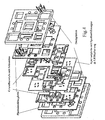
- eine Explosivdarstellung der einzelnen Bauteile des Pinholes
- Eine planare Struktur S des Grundbausteins besteht aus einem äußeren Rahmen R in den elastische schmale Stege ST eingearbeitet sind, die an ihren Gelenkstellen Aussparungen aufweisen, um die Verbindungsstellen klein und elastisch zu halten.
- Die Stege ST halten zwei innere Grundplatten G1 und G2, an denen zwei sich mit ihren parallelen Kanten gegenüberstehende Schneiden Sc1,2 befestigt sind. An die Grundplatten G1 und G2 sind seitlich Magnete M eines elektromagnetischen Aktuators befestigt, die in die im Rahmen R befestigten elektrische Spulen SP hineinragen.
- Durch elektrische Ansteuerung bewegen sich die Magnete in den Spulen und erzeugen dadurch eine Bewegung der Schneiden SC1, SC2 in Pfeilrichtung gegeneinander.
- Die elastischen Stege ST werden senkrecht zu ihrer Längsrichtung bewegt und sind in dieser Richtung elastisch an ihren Gelenkstellen, während die Anordnung senkrecht zur Bewegungsrichtung der Schneiden eine hohe Steifigkeit aufweist.
- Von der Positionskontrolle OPM sind hier nur die Dreiecke D1 und D2 für jede Schneide dargestellt. (siehe Fig. 3 und zugehörige Beschreibung).
- Fügt man nun zwei planare Grundbausteine nach Fig. 1 so zueinander, daß die Schneiden beider Grundbausteine zueinander einen Winkel, vorzugsweise 90 Grad einschließen, läßt sich durch jeweilige Veränderung des Abstandes der Schneidenkanten ein hochgenau variables Viereck, vorzugsweise ein Quadrat erzeugen , das als Pinhole in einem Laser- Scanning- Mikroskop dient.
- In Fig. 2 sind vergrößert der Magnet M und die elektrische Spule SP eines elektromagnetischen Aktuators dargestellt.
- In Fig. 3 ist das optische Meßsystem dargestellt.
- Hinter den entgegengesetzt ausgerichteten Dreiecken D1, D2, die in einer zur Verschieberichtung (Pfeil) senkrechten Reihe angeordnet sind, ist ein senkrecht zur Verschieberichtung orientierter Spalt AP angeordnet (Es kann sich auch um zwei Spalte handeln), die von einem oder bevorzugt zwei LEDs L1, L2 für jeweils eine Dreiecksöffnung beleuchtet werden.
- Durch die Schneidenbewegung verändert sich der Durchlaßbereich der Dreiecke D1, D2 in Bezug auf den Spalt oder die Spalte AP. Das bedeutet eine Veränderung der Lichtmenge, die von zwei Detektoren DE1, DE2 auf der anderen Seite entgegengesetzt der Lichtquellen separat für jedes Dreieck erfaßt werden.
- Ihre Lichtmengendifferenz bildet ein proportionales Stellsignal für den Verschiebeweg X, während die Summe der Detektorsignale gleich bleibt und somit das Signal in erster Näherung unabhängig von Lichtmengenschwankungen gewährleistet.
- Durch Erfassung der Stellsignale in X-und Y Richtung wird eine Information über den Öffnungszustand des Pinholes ermöglicht.
- Eine Eichung der Verstellanordnung kann durch externe Messung oder direkt in einem LSM erfolgen.
- Das Positionserfassungselement kann natürlich vorteilhaft auch über einen sonstigen, nicht optischen Sensor z.B. kapazitiven, induktiven oder elektromagnetischen Sensor realisiert werden, solange durch dieses Positionserfassungselement ein elektrisches Signal zur Rückkopplung bereitgestellt wird.
- In Fig.4 sind die einzelnen Elemente symmetrisch um die Aperturplatte mit Spaltenöffnungen angeordnet und bestehen aus 2 Grundbausteinen mit Schneiden zur mechanischen Pinholeöffnung, Photodetektorplatte für die Detektion der Lichtmengen und Deckplatte für elektronische Bauelemente und zur Abdeckung gegen Streulicht.
- Alle planaren Elemente sind durch Stifte positioniert und befestigt.
- Alle Elemente können durch verschiedenartige Bearbeitungsmethoden durch eine Vielzahl von Materialen realisiert werden, insbesondere metallische Materialen, Keramikmaterialien, Halbleiter und Kunststoffmaterialien.
Claims (7)
- Einstellbares Pinhole, insbesondere für den Beleuchtungs und/oder Detektionsstrahlengang eines Laser-Scanning-Mikroskopes, bestehend aus mindestens zwei planaren Grundbausteinen (S), bestehend aus einem äußeren Rahmen der stegartige Gelenkstellen (ST) aufweist, an denen mindestens eine in einer Richtung verschiebliche Schneide mit Schneidenkante (Sc1, Sc2) angebracht ist,
wobei die Grundbausteine zur optischen Erfassung der Position der mindestens einen Schneidenkante zwei asymmetrische Öffnungen (D1, D2) mit entgegengesetzter Orientierung, aufweisen, die von mindestens einer Lichtquelle (L1, L2) durchstrahlt werden, sowie aus einem vor oder hinter den Öffnungen vorzugsweise senkrecht zur Verschieberichtung der mindestens einen Schneidenkante orientierten Spalt (AP) durch den die Lichtmenge für jede asymmetrische Öffnung separat detektiert wird. - Pinhole nach Anspruch 1, wobei als Öffnungen zwei Dreiecke mit entgegengesetzter Orientierung vorgesehen sind.
- Pinhole nach Anspruch 1 oder 2,
wobei ein Grundbaustein zwei zueinander verschiebliche Schneidenkanten enthält, die zueinander einen vorzugsweise parallelen Zwischenraum einschließen. - Pinhole nach einem der Anspruche 1-3,
wobei zwei Grundbausteine mit je zwei Schneiden vorgesehen sind und die Verschieberichtung der Grundbausteine zueinander einen Winkel, vorzugsweise 90 Grad, einschließt. - Pinhole nach einem der Ansprüche 1-7,
wobei zum Antrieb der Verschiebung elektromagnetische Aktuatoren vorgesehen sind. - Einrichtung zur optischen Erfassung der Position und Öffnung eines Pinholes nach Anspruch 1 mit mindestens zwei zueinander in ihrer Lage veränderlichen Elementen (Sc1, Sc2), die zwischen sich eine veränderliche Lichtöffnung einschließen, insbesondere im Beleuchtungs- und/ oder Detektionsstrahlengang eines Laser- Scanning-Mikroskopes,
wobei zwei asymmetrische Öffnungen (D1, D2) mit im wesentlichen entgegengesetzter Orientierung vorgesehen sind, die von mindestens einer Lichtquelle (L1, L2) durchstrahlt werden und vor oder hinter den Öffnungen ein Spalt (AP) vorgesehen ist, Wobei die Lichtmenge durch den Spalt für jede Öffnung separat detektiert wird. - Einrichtung nach Anspruch 9, wobei die Position und Öffnung der Schneidenkanten über ein integriertes optisches Meßsystem in einem geschlossenen Regelkreis kontrolliert werden.
Applications Claiming Priority (2)
| Application Number | Priority Date | Filing Date | Title |
|---|---|---|---|
| DE10323922A DE10323922A1 (de) | 2003-05-22 | 2003-05-22 | Einstellbares Pinhole |
| PCT/EP2004/004498 WO2004104647A1 (de) | 2003-05-22 | 2004-04-28 | Einstellbares pinhole |
Publications (2)
| Publication Number | Publication Date |
|---|---|
| EP1625427A1 EP1625427A1 (de) | 2006-02-15 |
| EP1625427B1 true EP1625427B1 (de) | 2007-03-21 |
Family
ID=33441338
Family Applications (1)
| Application Number | Title | Priority Date | Filing Date |
|---|---|---|---|
| EP04729848A Expired - Lifetime EP1625427B1 (de) | 2003-05-22 | 2004-04-28 | Einstellbares pinhole |
Country Status (6)
| Country | Link |
|---|---|
| US (1) | US8077413B2 (de) |
| EP (1) | EP1625427B1 (de) |
| JP (1) | JP2007500872A (de) |
| AT (1) | ATE357676T1 (de) |
| DE (2) | DE10323922A1 (de) |
| WO (1) | WO2004104647A1 (de) |
Families Citing this family (5)
| Publication number | Priority date | Publication date | Assignee | Title |
|---|---|---|---|---|
| DE102005020542A1 (de) | 2005-05-03 | 2006-11-09 | Carl Zeiss Jena Gmbh | Einrichtung und Verfahren zur reproduzierbaren Einstellung der Pinholeöffnung und Pinholelage in Laserscanmikroskopen |
| JP4520918B2 (ja) * | 2005-08-12 | 2010-08-11 | 株式会社ミツトヨ | スリット幅調整装置およびこれを備えた顕微鏡レーザリペア装置 |
| DE102010036790A1 (de) * | 2010-08-02 | 2012-02-02 | Leica Microsystems Cms Gmbh | Einrichtung zur lückenlosen Einstellung von Spektrometer-Spaltbreiten |
| KR101682524B1 (ko) * | 2011-09-19 | 2016-12-06 | 참엔지니어링(주) | 슬릿 폭 조정 장치 |
| WO2018089864A1 (en) * | 2016-11-12 | 2018-05-17 | Caliber Imaging & Diagnostics, Inc. | Confocal microscope with positionable imaging head |
Family Cites Families (20)
| Publication number | Priority date | Publication date | Assignee | Title |
|---|---|---|---|---|
| US2964998A (en) * | 1958-10-03 | 1960-12-20 | Fred J Middlestadt | Precision light aperture arrangement |
| GB1327394A (en) * | 1969-10-23 | 1973-08-22 | Atomic Energy Authority Uk | Adjustable slits |
| US4017162A (en) * | 1973-08-13 | 1977-04-12 | Varian Techtron Pty. Ltd. | Adjustable slit mechanism |
| US4047808A (en) * | 1975-08-13 | 1977-09-13 | Varian Techtron Proprietary Limited | Adjustable slit mechanism |
| JPS6182649A (ja) * | 1984-09-29 | 1986-04-26 | Shimadzu Corp | スリツト機構 |
| JPH0789190B2 (ja) * | 1986-02-03 | 1995-09-27 | キヤノン株式会社 | 自動露出制御装置 |
| NL8700496A (nl) * | 1987-02-27 | 1988-09-16 | Stichting Tech Wetenschapp | Continu variabel microdiafragma. |
| JPH0618171B2 (ja) * | 1987-10-16 | 1994-03-09 | 日本電気株式会社 | アパーチャ絞り |
| JPH01116618A (ja) * | 1987-10-30 | 1989-05-09 | Nec Corp | 可変アパチャ |
| JP2785202B2 (ja) * | 1989-04-19 | 1998-08-13 | ソニー株式会社 | 光学式ディスク装置 |
| JPH0359935A (ja) * | 1989-07-27 | 1991-03-14 | Nippon X-Ray Kk | モータ直結形回転対陰極 |
| DE4110839A1 (de) * | 1991-04-04 | 1992-10-08 | Zeiss Carl Fa | Praezisionsspalt einstellbarer breite |
| DE4212077A1 (de) * | 1992-04-10 | 1993-10-14 | Fraunhofer Ges Forschung | Piezoelektrisch verstellbares Ventil und Verfahren zu ihrer Herstellung |
| EP0628796B1 (de) * | 1993-06-09 | 1996-08-28 | Hewlett-Packard GmbH | Regelbare optische Komponente |
| JPH0723855B2 (ja) * | 1993-09-01 | 1995-03-15 | 株式会社島津製作所 | 分光器スリット機構 |
| US6392703B1 (en) * | 1995-02-28 | 2002-05-21 | Canon Kabushiki Kaisha | Optical apparatus for forming an object image on a sensing element |
| JP3711586B2 (ja) * | 1995-06-02 | 2005-11-02 | 株式会社ニコン | 走査露光装置 |
| JPH09159935A (ja) * | 1995-12-12 | 1997-06-20 | Olympus Optical Co Ltd | 可変ピンホール機構 |
| DE69836030T2 (de) * | 1997-08-29 | 2007-01-11 | Olympus Optical Co., Ltd. | Mikroskop |
| DE20205079U1 (de) * | 2002-03-30 | 2002-06-13 | Leica Microsystems | Variable Lochblende und konfokales Scanmikroskop |
-
2003
- 2003-05-22 DE DE10323922A patent/DE10323922A1/de not_active Withdrawn
-
2004
- 2004-04-28 US US10/557,903 patent/US8077413B2/en not_active Expired - Fee Related
- 2004-04-28 DE DE502004003287T patent/DE502004003287D1/de not_active Expired - Lifetime
- 2004-04-28 AT AT04729848T patent/ATE357676T1/de not_active IP Right Cessation
- 2004-04-28 JP JP2006529719A patent/JP2007500872A/ja active Pending
- 2004-04-28 EP EP04729848A patent/EP1625427B1/de not_active Expired - Lifetime
- 2004-04-28 WO PCT/EP2004/004498 patent/WO2004104647A1/de not_active Ceased
Also Published As
| Publication number | Publication date |
|---|---|
| EP1625427A1 (de) | 2006-02-15 |
| JP2007500872A (ja) | 2007-01-18 |
| US20070285813A1 (en) | 2007-12-13 |
| US8077413B2 (en) | 2011-12-13 |
| DE502004003287D1 (de) | 2007-05-03 |
| ATE357676T1 (de) | 2007-04-15 |
| DE10323922A1 (de) | 2004-12-16 |
| WO2004104647A1 (de) | 2004-12-02 |
Similar Documents
| Publication | Publication Date | Title |
|---|---|---|
| DE19842364C1 (de) | Mikropolarimeter und Ellipsometer | |
| DE102008019600B4 (de) | Optische Vorrichtung in gestapelter Bauweise und Verfahren zur Herstellung derselben | |
| EP2642254B1 (de) | Anordnung mit einer ersten und einer zweiten Positionsmesseinrichtung | |
| EP1882153A1 (de) | Vorrichtung und verfahren zum vermessen von oberflächen | |
| EP0271646B1 (de) | Vorrichtung zur berührungsfreien Messung eines Abstandes von einer Oberfläche, insbesondere zur Abtastung einer Kontur einer Oberfläche eines Werkstückes länges eines Messweges | |
| WO2005121700A1 (de) | Vorrichtung und verfahren zum prüfen von oberflächen im inneren von löchern | |
| DE102011004477A1 (de) | Scanspiegelvorrichtung | |
| EP2977811A1 (de) | System mit einem piezoresistiven Positionssensor | |
| WO2003093892A1 (de) | Konfokales mikroskop mit zwei mikrolinsenarrays und einem lochblendenarray | |
| DE19830120A1 (de) | Optoelektronische Sensoreinrichtung | |
| EP2975369B1 (de) | Monochromator mit schwingungsarm bewegbaren optischen elementen | |
| EP1002221B1 (de) | Mikropolarimeter | |
| DE10323922A1 (de) | Einstellbares Pinhole | |
| EP3150970B1 (de) | Optisches schichtsystem | |
| DE2910588C2 (de) | Vorrichtung zum Empfang einer elektromagnetischen Strahlung | |
| EP1403674B1 (de) | Einstellbares Pinhole | |
| DE19621188A1 (de) | Optischer Sensor zur Bestimmung des Drehwinkels einer Drehachse | |
| DE19744938A1 (de) | Optische Positionsmeßeinrichtung | |
| EP1625359B1 (de) | Einstellbares pinhole, insbesondere für ein laser-scanning-mikroskop | |
| DE10357062A1 (de) | System zur optischen Bestimmung von Verkippungswinkeln an strukturierten Oberflächen | |
| EP2823263B1 (de) | Optoelektronische lagemessvorrichtung | |
| DE10329931A1 (de) | Planarer Direktantrieb mit einem Positionsmesssystem | |
| DE4316250A1 (de) | Lichtelektrische Längen- oder Winkelmeßeinrichtung | |
| DE102005016029A1 (de) | Vorrichtung und Verfahren zur Bestimmung der Fokuslage | |
| DE19621196C2 (de) | Optischer Sensor zum Verfolgen einer Zielmarke |
Legal Events
| Date | Code | Title | Description |
|---|---|---|---|
| PUAI | Public reference made under article 153(3) epc to a published international application that has entered the european phase |
Free format text: ORIGINAL CODE: 0009012 |
|
| 17P | Request for examination filed |
Effective date: 20051105 |
|
| AK | Designated contracting states |
Kind code of ref document: A1 Designated state(s): AT BE BG CH CY CZ DE DK EE ES FI FR GB GR HU IE IT LI LU MC NL PL PT RO SE SI SK TR |
|
| DAX | Request for extension of the european patent (deleted) | ||
| GRAP | Despatch of communication of intention to grant a patent |
Free format text: ORIGINAL CODE: EPIDOSNIGR1 |
|
| GRAS | Grant fee paid |
Free format text: ORIGINAL CODE: EPIDOSNIGR3 |
|
| GRAA | (expected) grant |
Free format text: ORIGINAL CODE: 0009210 |
|
| AK | Designated contracting states |
Kind code of ref document: B1 Designated state(s): AT BE BG CH CY CZ DE DK EE ES FI FR GB GR HU IE IT LI LU MC NL PL PT RO SE SI SK TR |
|
| PG25 | Lapsed in a contracting state [announced via postgrant information from national office to epo] |
Ref country code: IE Free format text: LAPSE BECAUSE OF FAILURE TO SUBMIT A TRANSLATION OF THE DESCRIPTION OR TO PAY THE FEE WITHIN THE PRESCRIBED TIME-LIMIT Effective date: 20070321 Ref country code: NL Free format text: LAPSE BECAUSE OF FAILURE TO SUBMIT A TRANSLATION OF THE DESCRIPTION OR TO PAY THE FEE WITHIN THE PRESCRIBED TIME-LIMIT Effective date: 20070321 Ref country code: SI Free format text: LAPSE BECAUSE OF FAILURE TO SUBMIT A TRANSLATION OF THE DESCRIPTION OR TO PAY THE FEE WITHIN THE PRESCRIBED TIME-LIMIT Effective date: 20070321 Ref country code: PL Free format text: LAPSE BECAUSE OF FAILURE TO SUBMIT A TRANSLATION OF THE DESCRIPTION OR TO PAY THE FEE WITHIN THE PRESCRIBED TIME-LIMIT Effective date: 20070321 Ref country code: FI Free format text: LAPSE BECAUSE OF FAILURE TO SUBMIT A TRANSLATION OF THE DESCRIPTION OR TO PAY THE FEE WITHIN THE PRESCRIBED TIME-LIMIT Effective date: 20070321 |
|
| REG | Reference to a national code |
Ref country code: GB Ref legal event code: FG4D Free format text: NOT ENGLISH |
|
| RIN1 | Information on inventor provided before grant (corrected) |
Inventor name: FAVRE, SEBASTIAN Inventor name: LOPEZ, ANTONIO Inventor name: GIANOTTI, RONALD Inventor name: SIDLER, THOMAS Inventor name: LASSER, THEO |
|
| REG | Reference to a national code |
Ref country code: CH Ref legal event code: EP |
|
| REF | Corresponds to: |
Ref document number: 502004003287 Country of ref document: DE Date of ref document: 20070503 Kind code of ref document: P |
|
| GBT | Gb: translation of ep patent filed (gb section 77(6)(a)/1977) |
Effective date: 20070412 |
|
| REG | Reference to a national code |
Ref country code: IE Ref legal event code: FG4D Free format text: LANGUAGE OF EP DOCUMENT: GERMAN |
|
| PG25 | Lapsed in a contracting state [announced via postgrant information from national office to epo] |
Ref country code: SE Free format text: LAPSE BECAUSE OF FAILURE TO SUBMIT A TRANSLATION OF THE DESCRIPTION OR TO PAY THE FEE WITHIN THE PRESCRIBED TIME-LIMIT Effective date: 20070621 |
|
| PG25 | Lapsed in a contracting state [announced via postgrant information from national office to epo] |
Ref country code: ES Free format text: LAPSE BECAUSE OF FAILURE TO SUBMIT A TRANSLATION OF THE DESCRIPTION OR TO PAY THE FEE WITHIN THE PRESCRIBED TIME-LIMIT Effective date: 20070702 |
|
| ET | Fr: translation filed | ||
| PG25 | Lapsed in a contracting state [announced via postgrant information from national office to epo] |
Ref country code: PT Free format text: LAPSE BECAUSE OF FAILURE TO SUBMIT A TRANSLATION OF THE DESCRIPTION OR TO PAY THE FEE WITHIN THE PRESCRIBED TIME-LIMIT Effective date: 20070821 |
|
| NLV1 | Nl: lapsed or annulled due to failure to fulfill the requirements of art. 29p and 29m of the patents act | ||
| REG | Reference to a national code |
Ref country code: IE Ref legal event code: FD4D |
|
| PG25 | Lapsed in a contracting state [announced via postgrant information from national office to epo] |
Ref country code: SK Free format text: LAPSE BECAUSE OF FAILURE TO SUBMIT A TRANSLATION OF THE DESCRIPTION OR TO PAY THE FEE WITHIN THE PRESCRIBED TIME-LIMIT Effective date: 20070321 |
|
| BERE | Be: lapsed |
Owner name: CARL ZEISS JENA G.M.B.H. Effective date: 20070430 |
|
| PG25 | Lapsed in a contracting state [announced via postgrant information from national office to epo] |
Ref country code: CZ Free format text: LAPSE BECAUSE OF FAILURE TO SUBMIT A TRANSLATION OF THE DESCRIPTION OR TO PAY THE FEE WITHIN THE PRESCRIBED TIME-LIMIT Effective date: 20070321 Ref country code: RO Free format text: LAPSE BECAUSE OF FAILURE TO SUBMIT A TRANSLATION OF THE DESCRIPTION OR TO PAY THE FEE WITHIN THE PRESCRIBED TIME-LIMIT Effective date: 20070321 |
|
| PLBE | No opposition filed within time limit |
Free format text: ORIGINAL CODE: 0009261 |
|
| STAA | Information on the status of an ep patent application or granted ep patent |
Free format text: STATUS: NO OPPOSITION FILED WITHIN TIME LIMIT |
|
| PG25 | Lapsed in a contracting state [announced via postgrant information from national office to epo] |
Ref country code: DK Free format text: LAPSE BECAUSE OF FAILURE TO SUBMIT A TRANSLATION OF THE DESCRIPTION OR TO PAY THE FEE WITHIN THE PRESCRIBED TIME-LIMIT Effective date: 20070321 |
|
| 26N | No opposition filed |
Effective date: 20071227 |
|
| PG25 | Lapsed in a contracting state [announced via postgrant information from national office to epo] |
Ref country code: BE Free format text: LAPSE BECAUSE OF NON-PAYMENT OF DUE FEES Effective date: 20070430 |
|
| PG25 | Lapsed in a contracting state [announced via postgrant information from national office to epo] |
Ref country code: GR Free format text: LAPSE BECAUSE OF FAILURE TO SUBMIT A TRANSLATION OF THE DESCRIPTION OR TO PAY THE FEE WITHIN THE PRESCRIBED TIME-LIMIT Effective date: 20070622 Ref country code: IT Free format text: LAPSE BECAUSE OF FAILURE TO SUBMIT A TRANSLATION OF THE DESCRIPTION OR TO PAY THE FEE WITHIN THE PRESCRIBED TIME-LIMIT Effective date: 20070321 |
|
| PG25 | Lapsed in a contracting state [announced via postgrant information from national office to epo] |
Ref country code: AT Free format text: LAPSE BECAUSE OF NON-PAYMENT OF DUE FEES Effective date: 20070428 |
|
| REG | Reference to a national code |
Ref country code: CH Ref legal event code: PL |
|
| PG25 | Lapsed in a contracting state [announced via postgrant information from national office to epo] |
Ref country code: LI Free format text: LAPSE BECAUSE OF NON-PAYMENT OF DUE FEES Effective date: 20080430 Ref country code: CH Free format text: LAPSE BECAUSE OF NON-PAYMENT OF DUE FEES Effective date: 20080430 Ref country code: EE Free format text: LAPSE BECAUSE OF FAILURE TO SUBMIT A TRANSLATION OF THE DESCRIPTION OR TO PAY THE FEE WITHIN THE PRESCRIBED TIME-LIMIT Effective date: 20070321 |
|
| PG25 | Lapsed in a contracting state [announced via postgrant information from national office to epo] |
Ref country code: MC Free format text: LAPSE BECAUSE OF NON-PAYMENT OF DUE FEES Effective date: 20070430 |
|
| PG25 | Lapsed in a contracting state [announced via postgrant information from national office to epo] |
Ref country code: CY Free format text: LAPSE BECAUSE OF FAILURE TO SUBMIT A TRANSLATION OF THE DESCRIPTION OR TO PAY THE FEE WITHIN THE PRESCRIBED TIME-LIMIT Effective date: 20070321 |
|
| PG25 | Lapsed in a contracting state [announced via postgrant information from national office to epo] |
Ref country code: LU Free format text: LAPSE BECAUSE OF NON-PAYMENT OF DUE FEES Effective date: 20070428 Ref country code: BG Free format text: LAPSE BECAUSE OF FAILURE TO SUBMIT A TRANSLATION OF THE DESCRIPTION OR TO PAY THE FEE WITHIN THE PRESCRIBED TIME-LIMIT Effective date: 20070621 |
|
| PG25 | Lapsed in a contracting state [announced via postgrant information from national office to epo] |
Ref country code: HU Free format text: LAPSE BECAUSE OF FAILURE TO SUBMIT A TRANSLATION OF THE DESCRIPTION OR TO PAY THE FEE WITHIN THE PRESCRIBED TIME-LIMIT Effective date: 20070922 Ref country code: TR Free format text: LAPSE BECAUSE OF FAILURE TO SUBMIT A TRANSLATION OF THE DESCRIPTION OR TO PAY THE FEE WITHIN THE PRESCRIBED TIME-LIMIT Effective date: 20070321 |
|
| REG | Reference to a national code |
Ref country code: DE Ref legal event code: R081 Ref document number: 502004003287 Country of ref document: DE Owner name: CARL ZEISS MICROSCOPY GMBH, DE Free format text: FORMER OWNER: CARL ZEISS JENA GMBH, 07745 JENA, DE Effective date: 20130724 |
|
| PGFP | Annual fee paid to national office [announced via postgrant information from national office to epo] |
Ref country code: GB Payment date: 20140422 Year of fee payment: 11 |
|
| PGFP | Annual fee paid to national office [announced via postgrant information from national office to epo] |
Ref country code: FR Payment date: 20140422 Year of fee payment: 11 Ref country code: DE Payment date: 20140418 Year of fee payment: 11 |
|
| REG | Reference to a national code |
Ref country code: DE Ref legal event code: R119 Ref document number: 502004003287 Country of ref document: DE |
|
| GBPC | Gb: european patent ceased through non-payment of renewal fee |
Effective date: 20150428 |
|
| PG25 | Lapsed in a contracting state [announced via postgrant information from national office to epo] |
Ref country code: GB Free format text: LAPSE BECAUSE OF NON-PAYMENT OF DUE FEES Effective date: 20150428 Ref country code: DE Free format text: LAPSE BECAUSE OF NON-PAYMENT OF DUE FEES Effective date: 20151103 |
|
| REG | Reference to a national code |
Ref country code: FR Ref legal event code: ST Effective date: 20151231 |
|
| PG25 | Lapsed in a contracting state [announced via postgrant information from national office to epo] |
Ref country code: FR Free format text: LAPSE BECAUSE OF NON-PAYMENT OF DUE FEES Effective date: 20150430 |