EP1624577B1 - Génération améeliorée de signaux analogiques en utilisant un modulateur delta-sigma - Google Patents
Génération améeliorée de signaux analogiques en utilisant un modulateur delta-sigma Download PDFInfo
- Publication number
- EP1624577B1 EP1624577B1 EP04103817A EP04103817A EP1624577B1 EP 1624577 B1 EP1624577 B1 EP 1624577B1 EP 04103817 A EP04103817 A EP 04103817A EP 04103817 A EP04103817 A EP 04103817A EP 1624577 B1 EP1624577 B1 EP 1624577B1
- Authority
- EP
- European Patent Office
- Prior art keywords
- delta
- sigma modulator
- bit
- discrete function
- sigma
- Prior art date
- Legal status (The legal status is an assumption and is not a legal conclusion. Google has not performed a legal analysis and makes no representation as to the accuracy of the status listed.)
- Expired - Fee Related
Links
Images


Classifications
-
- H—ELECTRICITY
- H03—ELECTRONIC CIRCUITRY
- H03M—CODING; DECODING; CODE CONVERSION IN GENERAL
- H03M7/00—Conversion of a code where information is represented by a given sequence or number of digits to a code where the same, similar or subset of information is represented by a different sequence or number of digits
- H03M7/30—Compression; Expansion; Suppression of unnecessary data, e.g. redundancy reduction
- H03M7/3002—Conversion to or from differential modulation
- H03M7/3004—Digital delta-sigma modulation
- H03M7/3013—Non-linear modulators
-
- H—ELECTRICITY
- H03—ELECTRONIC CIRCUITRY
- H03M—CODING; DECODING; CODE CONVERSION IN GENERAL
- H03M3/00—Conversion of analogue values to or from differential modulation
- H03M3/30—Delta-sigma modulation
- H03M3/322—Continuously compensating for, or preventing, undesired influence of physical parameters
- H03M3/324—Continuously compensating for, or preventing, undesired influence of physical parameters characterised by means or methods for compensating or preventing more than one type of error at a time, e.g. by synchronisation or using a ratiometric arrangement
- H03M3/344—Continuously compensating for, or preventing, undesired influence of physical parameters characterised by means or methods for compensating or preventing more than one type of error at a time, e.g. by synchronisation or using a ratiometric arrangement by filtering other than the noise-shaping inherent to delta-sigma modulators, e.g. anti-aliasing
-
- H—ELECTRICITY
- H03—ELECTRONIC CIRCUITRY
- H03M—CODING; DECODING; CODE CONVERSION IN GENERAL
- H03M3/00—Conversion of analogue values to or from differential modulation
- H03M3/30—Delta-sigma modulation
- H03M3/50—Digital/analogue converters using delta-sigma modulation as an intermediate step
-
- H—ELECTRICITY
- H03—ELECTRONIC CIRCUITRY
- H03M—CODING; DECODING; CODE CONVERSION IN GENERAL
- H03M7/00—Conversion of a code where information is represented by a given sequence or number of digits to a code where the same, similar or subset of information is represented by a different sequence or number of digits
- H03M7/30—Compression; Expansion; Suppression of unnecessary data, e.g. redundancy reduction
- H03M7/3002—Conversion to or from differential modulation
- H03M7/3004—Digital delta-sigma modulation
- H03M7/3015—Structural details of digital delta-sigma modulators
- H03M7/302—Structural details of digital delta-sigma modulators characterised by the number of quantisers and their type and resolution
- H03M7/3024—Structural details of digital delta-sigma modulators characterised by the number of quantisers and their type and resolution having one quantiser only
-
- H—ELECTRICITY
- H03—ELECTRONIC CIRCUITRY
- H03M—CODING; DECODING; CODE CONVERSION IN GENERAL
- H03M7/00—Conversion of a code where information is represented by a given sequence or number of digits to a code where the same, similar or subset of information is represented by a different sequence or number of digits
- H03M7/30—Compression; Expansion; Suppression of unnecessary data, e.g. redundancy reduction
- H03M7/3002—Conversion to or from differential modulation
- H03M7/3004—Digital delta-sigma modulation
- H03M7/3015—Structural details of digital delta-sigma modulators
- H03M7/3031—Structural details of digital delta-sigma modulators characterised by the order of the loop filter, e.g. having a first order loop filter in the feedforward path
Definitions
- the present invention relates to an improvement of signal integrity of analog signals based on the output of a delta-sigma modulator into which samples of the analog signal to be generated are fed.
- the filter following the delta-sigma modulator averages the bit stream of the mentioned driver and for an ideal signal integrity the contribution of each "high"-bit of the bit stream to the output signal must be equal, and the contribution of each "low”-bit of the bit stream to the output signal must be equal.
- memory effects in the driver circuit known as inter symbol interference (ISI)
- ISI inter symbol interference
- Settling time, slew-rate limitations, unequal rise-/fall-times and ringing are contributing to the inter symbol interference.
- the present invention relates also to improvements in the evaluation of a Device Under Test (DUT) in response to an input signal provided by an Automated Test Equipment (ATE) to said DUT, said input signal having improved integrity according to the inventive method and system.
- DUT Device Under Test
- ATE Automated Test Equipment
- Integrated Circuits generally need to be tested to assure proper operation. This - in particular - is required during IC development and manufacturing. In the latter case, the ICs are usually tested before final application. During test, the IC, as Device Under Test (DUT), is exposed to various types of stimulus signals, and its responses are measured, processed and usually compared to an expected response of a good device. Automated Test Equipments (ATE) usually perform these tasks according to a device-specific test program. Examples for ATE are the Agilent 83000 and 93000 families of Semiconductor Test Systems of Agilent Technologies as disclosed e.g. under http://www.ate.agilent.com/ste/products/intelligent test/SOC test/SOC Tech Oview.shtml.
- US-A-6,150,969 discloses a delta sigma modulator of at least second order which includes correction means applied to each feedback loop in the modulator, to account for systemic nonlinear output distortions. Since the output distortion is nonlinear, the correction applied to each feedback loop is nontrivially different.
- a corrected delta sigma modulator may be used in a demodulator including an output digital to analog converter (DAC) to account for systemic imperfections in the pulses formed by the DAC.
- DAC digital to analog converter
- the corrected delta sigma modulator is also useful in correcting output errors associated with high quality multilevel demodulators and class D power amplifiers.
- the corrected delta sigma modulator may be one bit or multilevel.
- US 6,404,369 B1 discloses a circuit topology and method for converting a digital input signal to an analog output signal which employs a modified sigma-delta loop and a DAC, and operates with improved accuracy over a wide frequency range.
- a loop filter such as a digital accumulator receives an input signal proportional to the difference between a digital input signal and a feedback signal.
- a quantizer quantizes the output of the loop filter, and the DAC converts the quantized signal into an analog output signal.
- the quantized signal is also provided to a DAC model.
- the DAC model varies the feedback signal to match expected output signals from the DAC, including errors introduced by the DAC. By the operation of the sigma-delta loop, the errors of the DAC are substantially reduced.
- Cataltepe T et al: "Digitally corrected multi-bit Sigma Delta data converters" IEEE International Symposium on Circuits and Systems, 8-11 May 1989, pages 647-650 , discloses sigma-delta converters using multi-bit internal A/D and D/A converters which have a low quantization noise. Digital correction schemes are used for to cancel errors due to nonlinearity of the internal DAC.
- US 6,232,899 B1 describes a signal converter comprising a pulse modulator, and means for modifying the signal input thereto in dependence upon the error in previous values of the output thereof, to reduce the effects of said error within a desired signal band.
- the present invention also relates to general test equipment as well as all types of analog signal generation.
- ISI inter symbol interference
- the objects are achieved by modifying the feedback loop of said delta-sigma modulator, more particular, by introducing a non-linear, time-discrete function modeling the effect of inter signal interference (ISI) using a model initially based on measurement or simulation.
- ISI inter signal interference
- a method is provided of optimizing the mentioned non-linear, time-discrete function i.e. optimizing the mentioned model for best signal integrity of an output signal.
- the objects of the invention are achieved by modeling the effects of inter signal interference (ISI).
- ISI inter signal interference
- the result of this modeling is a non-linear, time-discrete function which may be presented by a look-up table comprising arguments and values of said non-linear, time-discrete function.
- the look-up table Dependent upon the current and previous bits the look-up table will supply a value to be used within a feedback loop of the delta-sigma modulator.
- One goal of this compensation is the equality of the contribution to the output signal of the delta-sigma modulator digital-to-analog converter of each "high"-bit and the equality of the contribution to the output of the delta-sigma modulator digital-to-analog converter of each "low”-bit.
- a first step the contribution of a current bit value under conditions which are different depending upon the history of previous bits is measured and/or simulated in order to determine initial values of the non-linear, time-discrete function.
- the arguments of the non-linear, time-discrete function comprise the current bit and at least one bit previous to the current bit.
- the initial values are optimized.
- the second step uses the initial values to generate a predetermined waveform, for example a sine wave, with a delta-sigma modulator digital-to-analog converter.
- the deviation of the generated analog signal from the ideal signal is evaluated, e.g. harmonics of a generated sine wave are measured and the values of the non-linear, time-discrete function in the look-up table are optimized for best analog signal integrity, e.g. for best suppression of harmonics in the case of a sine wave.
- the feedback loop of a delta-sigma modulator includes the non-linear, time-discrete function, e.g. as represented by the look-up table.
- the current output bit and at least one bit previous to the respective current bit of the delta-sigma modulator represent the arguments of the non-linear, time-discrete function.
- the values of previous bits are provided by serially connected delay elements.
- a multi-bit delta-sigma digital-to-analog converter for at least two, preferably for each driver, an individual non-linear, time-discrete function is introduced and thus compensation within the feedback loop will be done individually for each respective driver.
- the implementation of the method described within this disclosure may be either in hardware or in software.
- a band-pass delta-sigma digital-to-analog converter may be used in conjunction with the present invention.
- the inventive method can be used for generating analog signals with high signal integrity provided by an ATE to a DUT. Thus the performance evaluation of the DUT is more reliable.
- the present invention also relates to a software program or product for executing the method for generating an analog signal when running on a data processing system such as a computer.
- the program or product is stored on a data carrier.
- the present invention relates to a system generating an analog signal according to the present invention.
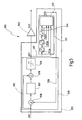
- Fig. 1 shows the main components of a single-bit delta-sigma digital-to-analog converter 1 without the inventive modification in the feedback loop.
- a single-bit delta-sigma modulator 2 is followed by a driver 3 and a low pass filter 4.
- a difference amplifier element representing a delta element 6 of the delta-sigma modulator 2
- a loop filter 7 an adder 8 representing a sigma element of the delta-sigma modulator 2
- a single-bit quantizer 9 a feed-forward line 95 and a feedback line 96.
- the desired analog signal is represented by a sequence of samples x[k] at the input of the delta-sigma modulator 2.
- a quantized pulse density modulated signal q[k] is provided which is fed into driver 3 and the output signal D(t) of driver 3 is fed into the low pass filter 4.
- the generated analog signal x(t) is available.
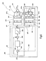
- Fig. 2 shows the main components of a multi-bit delta-sigma digital-to-analog converter 211 without the inventive modification in the feedback loop.
- the multi-bit delta-sigma digital-to-analog converter 211 comprising the main building blocks of a multi-bit delta-sigma modulator 212, a multi-bit digital-to-analog converter 213 and a low pass filter 204.
- a lower part of Fig. 2 an expanded view of the multi-bit delta-sigma modulator 212 is shown.
- an expanded view of the multi-bit digital-to-analog converter 213 is shown, which is preferably realized as a flash digital-to-analog converter with dynamic element matching (DEM).
- DEM dynamic element matching
- the multi-bit delta-sigma modulator 212 comprises a difference amplifier element 206, a loop filter 207 and an adder 208 as well as feedback line 296 and a feed-forward line 295 like known from fig. 1 .
- the quantizer 291 is a multi-bit quantizer.
- the multi-bit digital-to-analog converter 213 it comprises a decoder 271 with output lines 272 feeding a scrambler 273.
- Output lines 274 of the scrambler 273 are fed into the driver inputs 275a, 275b ... 275n.
- the output lines 276 of the drivers 275a, 275 b, ... 275n are followed by an adder 277.
- the desired analog signal is represented by a sequence of samples x[k] at the input of the delta-sigma modulator 212.
- a quantized pulse density modulated signal q[k] is provided which is fed into digital-to-analog converter 213 and the output signal D(t) of digital-to-analog converter 213 is fed into the low pass filter 204.
- the generated analog signal x(t) is available.
- Fig. 3 shows a diagram illustrating the areas under bits.
- the x-axis 321 is used to lay off time t and a bit period is marked by the unit marker 323. Dotted lines parallel to the y-axis 322 mark the begin and end of bit periods.
- the y-axis 322 shows qualitatively the signal level of signal D(t).
- A1, A2, A3 and A4 designate the areas under four consecutive bits.
- the low pass filter 4, as for example shown in fig. 1 averages the bit stream of a driver 3 in fig. 1 .
- Fig. 3 shows a diagram 320 of four possible waveforms Da(t) to Dd(t) of the output signal D(t) of the driver 3 for sequences of bits q[k] fed into the input of the driver 3.
- Time t is layed off as the x-axis 321 and the unit of one bit period 323 is marked.
- the level of the waveforms Da(t) to Dd(t) is layed off as the y-axis 322.
- the first waveform Da(t) results from a sequence "1-0” wherein the value is "1" within the first bit period A1.
- the second waveform Db(t) results from a sequence "1-1-0” wherein the value is "1" within the first and second bit periods A1 and A2.
- the third waveform Dc(t) results from a sequence "1-1-1-0” wherein the value is “1” within the first to third bit periods A1 to A3.
- the fourth waveform Dd(t) results from a sequence "1-1-1-1-0” wherein the value is "1” within the first to fourth bit periods A1 to A4. For t ⁇ 0 it is assumed that the value has been "0" for a long time.
- the contribution of a bit value "1" to the output signal D(t) of driver 3 depends on the history of previous bits.
- the contribution of the bit value "1" in the second period A2 within the signal Db(t) differs from the contribution of the bit value "1" in the first period A1 within the signal Db(t).
- bit values "1" For ideal signal integrity the contribution of bit values "1" should be independent upon the history of previous bits. Thus it is advantageous if for same bit values "1" or “0" areas under the waveform of driver output signal D(t) within a bit period are equal, independent upon the history of previous bits.
- memory effects in drivers also known as inter symbol interference (ISI), make pulse form of one bit and thus area under pulse or bit dependent upon history of previous bits. Effects that are contributing to inter symbol interference are for example settling time, slew-rate limitations, unequal rise-/fall-times and ringing.
- Fig. 4 shows a tabular representation 430 of an example of a non-linear time-discrete function used for compensation in the modified feedback loop of embodiments of the present invention for the case of a history of two previous bits q[k-1] and q[k-2] taken into account.
- the values given for a[k] in fig. 4 are chosen only for demonstration. A tendency can be recognized in a way that the value a[k] is a maximum of "+1", if q[k] is "1" as well as q[k-1] and q[k-2], and is a minimum of "-1", if q[k] is "0” as well as q[k-1] and q[k-2]. It has to be noted that a[k] is substracted by the delta element of the delta-sigma modulator from samples x[k].
- Fig. 5 shows a first embodiment 599 of the present invention. Comparing fig. 5 with fig. 1 clearly shows the modification of the feedback loop.
- the feedback loop 96 connects the output of the quantizer 9 directly to the input of the difference amplifier element 6.
- the feedback loop is split into a first part 597 of the feedback loop connected to the output q[k] of the quantizer 509 and feeding this output q[k] into the inter symbol interference (ISI) driver model 551 representing the non-linear time-discrete function to be introduced in the feedback loop.
- the output a[k] of the inter symbol interference driver model 551 is fed into a difference amplifier element representing the delta element 506 of the delta-sigma modulator via the second part 598 of the feedback line.
- a feed-forward line 595 connects the input signal x[k] to the adder representing the sigma element 508 of the delta-sigma modulator.
- the output signal of the delta element 506 is fed into a loop filter 507.
- Output of the loop filter 507 is fed into the sigma element 508.
- the output signal q[k] of the quantizer 509 is fed into the driver 503.
- the signal D(t) is present.
- Parts of the main building blocks of this first embodiment 599 are grouped showing parts of a single-bit delta-sigma modulator 505 without the inventive modification in the feedback loop, parts of the inter symbol interference (ISI) driver model 551 and the combination of these both groups forming an inventive delta-sigma modulator 552 of the first embodiment 599 of the invention.
- ISI inter symbol interference
- the inter symbol interference driver model 551 comprises one-clock-period delay elements 553a, 553b, ... 553n driven by the output q[k] of the quantizer 509 via the first part 597 of the feedback line.
- Output signals of the one-clock-period delay elements 553a, 553b, ... 553n are fed via the control word lines 554 into the look-up table 555.
- the output a[k] of the look-up table 555 instead of the original output signal q[k] of the quantizer 509 is fed back into a difference amplifier element representing the delta element 506 of the delta-sigma modulator.
- the feedback loop is modified such that the modeled area contribution of each bit is fed back instead of the ideal bit value.
- Fig. 6 shows a second embodiment of the present invention presenting a block diagram of a multi-bit delta-sigma digital-to-analog converter 699. Comparing fig. 6 with fig. 2 shows that the feedback line 296 shown in fig. 2 now in fig. 6 is split into two parts, wherein a first part 697 of the feedback line feeds the multi-bit driver inter symbol interference model 661. Output of the multi-bit driver inter symbol interference model 661 is fed via the second part 698 of the feedback line to the difference amplifier element 606.
- the second embodiment comprises several driver inter symbol interference models 667a, 667b ... 667n within the multi-bit driver inter symbol interference model 661. Each of these models represent the compensation needed to compensate for non idealities of the corresponding drivers 675a, 675b, ... 675n.
- Parts of the main building blocks of this second embodiment 699 are grouped showing parts of a multi-bit delta-sigma modulator 615 without the inventive modification in the feedback loop, parts of the muti-bit inter symbol interference (ISI) driver model 661 and the combination of these both groups forming an inventive multi-bit delta-sigma modulator 689 of the second embodiment 699 of the invention.
- ISI inter symbol interference
- this embodiment comprises a decoder 671 with output lines 672 feeding a scrambler 673.
- Output lines 674 of the scrambler 673 are fed into the driver inputs 675a, 675b ... 675n.
- the output lines 676 of the drivers 675a, 675b ... 675n are fed into an adder 677.
- the signal D(t) is present.
- the multi-bit driver inter symbol interference model 661 comprises a decoder 662 with output lines 663 feeding a scrambler 664.
- Output lines 665 of the scrambler 664 are fed into the individual driver inter symbol interference (ISI) models 667a, 667b ... 667n.
- Output signals a1[k], a2[k]... a3[k] of the individual driver inter symbol interference (ISI) models 667a, 667b ... 667n are fed into an adder 669 using the lines 668.
- the output signal of adder 669 is fed into the delta element 606 using the second part 668 of the feedback line.
- the multi-bit delta-sigma modulator 615 comprises a difference amplifier element 606, a loop filter 607 and an adder 608 as well as feed-forward line 695 and a multi-bit quantizer 691.
Landscapes
- Engineering & Computer Science (AREA)
- Theoretical Computer Science (AREA)
- Physics & Mathematics (AREA)
- Nonlinear Science (AREA)
- Compression, Expansion, Code Conversion, And Decoders (AREA)
Claims (8)
- Procédé de génération d'un signal analogique x(t) sur base d'échantillons x[k] représentant ledit signal analogique, ledit procédé comprenant l'étape consistant à:alimenter lesdits échantillons x[k] vers un modulateur delta-sigma (552; 689), ledit modulateur delta-sigma (552; 689) sortant une séquence de bits q[k],caractérisé par les étapes suivantes:alimenter la séquence de bits q[k] vers une chaîne d'éléments de temporisation (553a à 553n);alimenter les signaux de sortie (554) des éléments de temporisation (553a à 553n) vers un tableau de consultation (555) mémorisant des combinaisons d'arguments et de values d'une fonction discrète dans le temps non linéaire;utiliser le tableau de consultation (555) pour déterminer une valeur a[k] de la fonction discrète dans le temps non linéaire en réponse aux signaux de sortie (554) des éléments de temporisation (553a à 553n); etfournir la valeur a[k] comme rétroaction vers le modulateur delta-sigma (552; 689),dans lequel ladite fonction discrète dans le temps non linéaire représente un modèle des non-idéalités d'au moins un pilote numérique à la sortie dudit modulateur delta-sigma (552; 689).
- Procédé selon la revendication 1, caractérisé par le fait que ladite fonction discrète dans le temps non linéaire est déterminée par une étape initiale résultant en des valeurs initiales de ladite fonction discrète dans le temps non linéaire, et une étape d'optimisation modifiant lesdites valeurs initiales, pour minimiser les écarts dudit signal analogique généré x(t) par rapport à un signal idéal correspondant.
- Procédé selon la revendication 1 ou 2, caractérisé par le fait que ledit modulateur delta-sigma (552; 689) est un modulateur delta-sigma multi-bit (689) suivi d'un décodeur (671) et d'un brouilleur (673).
- Procédé selon la revendication 3, caractérisé par le fait que ledit modulateur delta-sigma multi-bit (689) comprend une pluralité de pilotes (675a, 675b, ... 675n), et que, pour au moins deux des pilotes, une fonction discrète dans le temps non linéaire individuelle est introduite dans ladite boucle de rétroaction.
- Procédé selon la revendication 1 ou l'une quelconque des revendications ci-dessus, caractérisé par le fait que ledit modulateur delta-sigma (552; 689) est un modulateur delta-sigma passe-bande et est suivi d'un filtre passe-bande, formant ainsi un convertisseur numérique-analogique delta-sigma passe-bande.
- Procédé selon la revendication 1 ou l'une quelconque des revendications ci-dessus, caractérisé par le fait que ledit signal analogique x(t) généré est fourni par un Matériel de Test Automatisé comme signal d'entrée d'un Dispositif Testé.
- Programme ou produit de logiciel, de préférence mémorisé sur un support de données, pour réaliser le procédé selon la revendication 1 ou l'une quelconque des revendications ci-dessus lorsqu'il est exécuté sur un système de traitement de données tel qu'un ordinateur.
- Système de génération d'un signal analogique x(t) sur base d'échantillons x[k] représentant ledit signal analogique, ledit système comprenant:un modulateur delta-sigma (552; 689) sortant une séquence de bits q[k] en réponse auxdits échantillons x[k],caractérisé parune chaîne d'éléments de temporisation (553a à 553n) entraînés par la séquence de bits q[k]; etun tableau de consultation (555) connecté aux sorties des éléments de temporisation (553a à 553n) et au modulateur delta-sigma (552; 689), le tableau de consultation (555) mémorisant des combinaisons d'arguments et de valeurs d'une fonction discrète dans le temps non linéaire, opérationnel pour déterminer une valeur a[k] de la fonction discrète dans le temps non linéaire en réponse aux signaux de sortie (554) des éléments de temporisation (553a à 553n), et opérationnel pour fournir la valeur a[k] comme rétroaction au modulateur delta-sigma (552; 689), dans lequel ladite fonction discrète dans le temps non linéaire représente un modèle des non idéalités d'au moins un pilote numérique à la sortie dudit modulateur delta-sigma (552; 689).
Priority Applications (4)
| Application Number | Priority Date | Filing Date | Title |
|---|---|---|---|
| DE602004015276T DE602004015276D1 (de) | 2004-08-06 | 2004-08-06 | Verbesserte Analogsignalerzeugung mittels eines Delta-Sigma Modulators |
| EP04103817A EP1624577B1 (fr) | 2004-08-06 | 2004-08-06 | Génération améeliorée de signaux analogiques en utilisant un modulateur delta-sigma |
| JP2005219316A JP4451821B2 (ja) | 2004-08-06 | 2005-07-28 | デルタシグマ変調器を使用した、改良されたアナログ信号の生成 |
| US11/197,252 US7230556B2 (en) | 2004-08-06 | 2005-08-04 | Analog signal generation using a delta-sigma modulator |
Applications Claiming Priority (1)
| Application Number | Priority Date | Filing Date | Title |
|---|---|---|---|
| EP04103817A EP1624577B1 (fr) | 2004-08-06 | 2004-08-06 | Génération améeliorée de signaux analogiques en utilisant un modulateur delta-sigma |
Publications (2)
| Publication Number | Publication Date |
|---|---|
| EP1624577A1 EP1624577A1 (fr) | 2006-02-08 |
| EP1624577B1 true EP1624577B1 (fr) | 2008-07-23 |
Family
ID=34929429
Family Applications (1)
| Application Number | Title | Priority Date | Filing Date |
|---|---|---|---|
| EP04103817A Expired - Fee Related EP1624577B1 (fr) | 2004-08-06 | 2004-08-06 | Génération améeliorée de signaux analogiques en utilisant un modulateur delta-sigma |
Country Status (4)
| Country | Link |
|---|---|
| US (1) | US7230556B2 (fr) |
| EP (1) | EP1624577B1 (fr) |
| JP (1) | JP4451821B2 (fr) |
| DE (1) | DE602004015276D1 (fr) |
Families Citing this family (13)
| Publication number | Priority date | Publication date | Assignee | Title |
|---|---|---|---|---|
| US7605732B2 (en) * | 2007-01-29 | 2009-10-20 | Texas Instruments Incorporated | Systems and methods for kickback reduction in an ADC |
| US7554473B2 (en) * | 2007-05-02 | 2009-06-30 | Cirrus Logic, Inc. | Control system using a nonlinear delta-sigma modulator with nonlinear process modeling |
| US7659841B1 (en) | 2008-08-07 | 2010-02-09 | Actel Corporation | Quadratic and cubic compensation of sigma-delta D/A and A/D converters |
| EP2340613B1 (fr) * | 2008-10-23 | 2013-09-04 | Nxp B.V. | Modulateur sigma-delta |
| US8665128B2 (en) * | 2010-12-08 | 2014-03-04 | National Semiconductor Corporation | Sigma-delta difference-of-squares log-RMS to DC converter with forward path multiplier and chopper stabilization |
| US8665126B2 (en) * | 2010-12-08 | 2014-03-04 | National Semiconductor Corporation | ΣΔ difference-of-squares LOG-RMS to DC converter with forward and feedback paths signal squaring |
| US10530372B1 (en) | 2016-03-25 | 2020-01-07 | MY Tech, LLC | Systems and methods for digital synthesis of output signals using resonators |
| US10020818B1 (en) | 2016-03-25 | 2018-07-10 | MY Tech, LLC | Systems and methods for fast delta sigma modulation using parallel path feedback loops |
| US10367522B2 (en) | 2016-11-21 | 2019-07-30 | MY Tech, LLC | High efficiency power amplifier architectures for RF applications |
| JP6932439B2 (ja) * | 2017-07-11 | 2021-09-08 | 日本無線株式会社 | デジタル信号処理装置 |
| US10211848B1 (en) | 2018-03-27 | 2019-02-19 | Synaptics Incorporated | Delta sigma modulator systems and methods |
| JP7213947B2 (ja) * | 2019-02-26 | 2023-01-27 | 京セラ株式会社 | デルタシグマ変調装置及び通信機器 |
| US11933919B2 (en) | 2022-02-24 | 2024-03-19 | Mixed-Signal Devices Inc. | Systems and methods for synthesis of modulated RF signals |
Family Cites Families (16)
| Publication number | Priority date | Publication date | Assignee | Title |
|---|---|---|---|---|
| GB9103777D0 (en) * | 1991-02-22 | 1991-04-10 | B & W Loudspeakers | Analogue and digital convertors |
| EP0541839B1 (fr) | 1991-11-11 | 1993-07-28 | Hewlett-Packard GmbH | Appareil pour générer des signaux de test |
| DE4305442C2 (de) | 1993-02-23 | 1999-08-05 | Hewlett Packard Gmbh | Verfahren und Vorrichtung zum Erzeugen eines Testvektors |
| US6150969A (en) * | 1996-06-12 | 2000-11-21 | Audiologic, Incorporated | Correction of nonlinear output distortion in a Delta Sigma DAC |
| EP0882991B1 (fr) | 1997-05-22 | 1999-03-17 | Hewlett-Packard Company | Circuit de décompression |
| EP0886214B1 (fr) | 1997-05-30 | 1999-10-20 | Hewlett-Packard Company | Architecture multi-canal avec un signal d'horloge indépendant par canal |
| EP0859318B1 (fr) | 1997-09-13 | 1999-07-14 | Hewlett-Packard Company | Organisation optimisée de la mémoire dans une architecture d'ordinateur à canaux multiples |
| EP0864977B1 (fr) | 1997-09-13 | 1999-07-14 | Hewlett-Packard Company | Compensation du temps de latence d'une mémoire |
| US6249237B1 (en) * | 1998-10-09 | 2001-06-19 | Lsi Logic Corporation | System and method for bandpass shaping in an oversampling converter |
| US6414614B1 (en) * | 1999-02-23 | 2002-07-02 | Cirrus Logic, Inc. | Power output stage compensation for digital output amplifiers |
| EP1092983B1 (fr) | 2000-06-16 | 2003-01-22 | Agilent Technologies, Inc. (a Delaware corporation) | Testeur de circuits intégrés équipé d'une fonctionnalité de test multi-ports |
| US6404369B1 (en) * | 2000-09-29 | 2002-06-11 | Teradyne, Inc. | Digital to analog converter employing sigma-delta loop and feedback DAC model |
| US6946983B2 (en) * | 2002-04-26 | 2005-09-20 | Telefonaktiebolaget L M Ericcson | Digital-to-analog converter having error correction |
| SE523353C2 (sv) * | 2002-04-26 | 2004-04-13 | Ericsson Telefon Ab L M | Digital-/Analogomvandlare med felkompensering |
| US6819276B1 (en) * | 2003-05-13 | 2004-11-16 | Analog Devices, Inc. | Noise-shaper system and method |
| JP4856363B2 (ja) * | 2003-05-22 | 2012-01-18 | アギア システムズ インコーポレーテッド | 安定な高次デルタ・シグマ誤差フィードバック変調器およびそのような変調器において使用される雑音伝達関数 |
-
2004
- 2004-08-06 DE DE602004015276T patent/DE602004015276D1/de active Active
- 2004-08-06 EP EP04103817A patent/EP1624577B1/fr not_active Expired - Fee Related
-
2005
- 2005-07-28 JP JP2005219316A patent/JP4451821B2/ja not_active Expired - Fee Related
- 2005-08-04 US US11/197,252 patent/US7230556B2/en active Active
Also Published As
| Publication number | Publication date |
|---|---|
| DE602004015276D1 (de) | 2008-09-04 |
| EP1624577A1 (fr) | 2006-02-08 |
| JP4451821B2 (ja) | 2010-04-14 |
| JP2006050616A (ja) | 2006-02-16 |
| US20060028364A1 (en) | 2006-02-09 |
| US7230556B2 (en) | 2007-06-12 |
Similar Documents
| Publication | Publication Date | Title |
|---|---|---|
| US7230556B2 (en) | Analog signal generation using a delta-sigma modulator | |
| US6150969A (en) | Correction of nonlinear output distortion in a Delta Sigma DAC | |
| US7894536B2 (en) | Calibration model to mitigate data conversion errors | |
| KR100276013B1 (ko) | 아날로그/디지탈컨버터 | |
| EP1354410B1 (fr) | Convertisseur numerique-analogique utilisant une boucle sigma-delta et un modele de can a retroaction | |
| AU2005228167A1 (en) | Reduced complexity nonlinear filters for analog-to-digital converter linearization | |
| US5905453A (en) | Dithered sigma delta modulator having programmable full scale range adjustment | |
| WO2012166821A2 (fr) | Circuit de domaine de pointe et procédé de modélisation | |
| WO2000035097A1 (fr) | Etalonnage et compensation des delta-sigma de can et de cna au moyen de la correlation des signaux de bruit | |
| US5781138A (en) | System and method for generating a sigma-delta correction circuit | |
| IL90796A (en) | Digital correction circuit for data bearings | |
| US20050007266A1 (en) | Sigma-delta modulator with PWM output | |
| US6232897B1 (en) | System and method for calibrating an analog to digital converter through stimulation of current generators | |
| CN108809319A (zh) | 数/模转换器及操作方法 | |
| JP4699510B2 (ja) | D/a変換器 | |
| Kasher et al. | Memory-efficient SFDR-optimized post-correction of analog-to-digital converters via frequency-selective look-up tables | |
| US5955979A (en) | System and method for compensating for glitch errors in a D/A converter | |
| CA2246483C (fr) | Correction des erreurs dans la fonction de transfert d'un systeme au moyen d'une compensation d'entree | |
| JP3807036B2 (ja) | ディジタルデータ処理装置及び方法 | |
| JPH05284033A (ja) | Σδ変調器 | |
| van Rijt et al. | Learning control applied to a digital-to-analogue converter | |
| JPH04302223A (ja) | 回路装置 | |
| JPH06125274A (ja) | A/dコンバータの冗長性機能試験回路およびその方法 | |
| JP2874218B2 (ja) | A−dコンバータ | |
| CN117792397A (zh) | 数字-模拟转换器毛刺抑制技术 |
Legal Events
| Date | Code | Title | Description |
|---|---|---|---|
| PUAI | Public reference made under article 153(3) epc to a published international application that has entered the european phase |
Free format text: ORIGINAL CODE: 0009012 |
|
| AK | Designated contracting states |
Kind code of ref document: A1 Designated state(s): AT BE BG CH CY CZ DE DK EE ES FI FR GB GR HU IE IT LI LU MC NL PL PT RO SE SI SK TR |
|
| AX | Request for extension of the european patent |
Extension state: AL HR LT LV MK |
|
| 17P | Request for examination filed |
Effective date: 20060808 |
|
| AKX | Designation fees paid |
Designated state(s): DE FR GB |
|
| RAP1 | Party data changed (applicant data changed or rights of an application transferred) |
Owner name: AGILENT TECHNOLOGIES, INC. |
|
| 17Q | First examination report despatched |
Effective date: 20070508 |
|
| RAP1 | Party data changed (applicant data changed or rights of an application transferred) |
Owner name: VERIGY (SINGAPORE) PTE. LTD. |
|
| GRAP | Despatch of communication of intention to grant a patent |
Free format text: ORIGINAL CODE: EPIDOSNIGR1 |
|
| GRAS | Grant fee paid |
Free format text: ORIGINAL CODE: EPIDOSNIGR3 |
|
| GRAA | (expected) grant |
Free format text: ORIGINAL CODE: 0009210 |
|
| AK | Designated contracting states |
Kind code of ref document: B1 Designated state(s): DE FR GB |
|
| REG | Reference to a national code |
Ref country code: GB Ref legal event code: FG4D |
|
| REF | Corresponds to: |
Ref document number: 602004015276 Country of ref document: DE Date of ref document: 20080904 Kind code of ref document: P |
|
| PLBE | No opposition filed within time limit |
Free format text: ORIGINAL CODE: 0009261 |
|
| STAA | Information on the status of an ep patent application or granted ep patent |
Free format text: STATUS: NO OPPOSITION FILED WITHIN TIME LIMIT |
|
| GBPC | Gb: european patent ceased through non-payment of renewal fee |
Effective date: 20081023 |
|
| 26N | No opposition filed |
Effective date: 20090424 |
|
| PGFP | Annual fee paid to national office [announced via postgrant information from national office to epo] |
Ref country code: FR Payment date: 20090814 Year of fee payment: 6 |
|
| PG25 | Lapsed in a contracting state [announced via postgrant information from national office to epo] |
Ref country code: GB Free format text: LAPSE BECAUSE OF NON-PAYMENT OF DUE FEES Effective date: 20081023 |
|
| REG | Reference to a national code |
Ref country code: FR Ref legal event code: ST Effective date: 20110502 |
|
| PG25 | Lapsed in a contracting state [announced via postgrant information from national office to epo] |
Ref country code: FR Free format text: LAPSE BECAUSE OF NON-PAYMENT OF DUE FEES Effective date: 20100831 |
|
| REG | Reference to a national code |
Ref country code: DE Ref legal event code: R082 Ref document number: 602004015276 Country of ref document: DE Representative=s name: SCHOPPE, ZIMMERMANN, STOECKELER, ZINKLER & PAR, DE |
|
| REG | Reference to a national code |
Ref country code: DE Ref legal event code: R082 Ref document number: 602004015276 Country of ref document: DE Representative=s name: SCHOPPE, ZIMMERMANN, STOECKELER, ZINKLER & PAR, DE Effective date: 20120515 Ref country code: DE Ref legal event code: R081 Ref document number: 602004015276 Country of ref document: DE Owner name: ADVANTEST (SINGAPORE) PTE. LTD., SG Free format text: FORMER OWNER: VERIGY (SINGAPORE) PTE. LTD., SINGAPORE, SG Effective date: 20120515 Ref country code: DE Ref legal event code: R082 Ref document number: 602004015276 Country of ref document: DE Representative=s name: SCHOPPE, ZIMMERMANN, STOECKELER, ZINKLER, SCHE, DE Effective date: 20120515 |
|
| PGFP | Annual fee paid to national office [announced via postgrant information from national office to epo] |
Ref country code: DE Payment date: 20140730 Year of fee payment: 11 |
|
| REG | Reference to a national code |
Ref country code: DE Ref legal event code: R119 Ref document number: 602004015276 Country of ref document: DE |
|
| PG25 | Lapsed in a contracting state [announced via postgrant information from national office to epo] |
Ref country code: DE Free format text: LAPSE BECAUSE OF NON-PAYMENT OF DUE FEES Effective date: 20160301 |