EP1624342A2 - Lithographischer Apparat, ein Beleuchtungssystem enthältender Apparat, ein Projektionssystem enthältender Apparat, optisches Element für einen lithographischen Apparat und Verfahren zur Herstellung einer Vorrichtung - Google Patents
Lithographischer Apparat, ein Beleuchtungssystem enthältender Apparat, ein Projektionssystem enthältender Apparat, optisches Element für einen lithographischen Apparat und Verfahren zur Herstellung einer Vorrichtung Download PDFInfo
- Publication number
- EP1624342A2 EP1624342A2 EP05076746A EP05076746A EP1624342A2 EP 1624342 A2 EP1624342 A2 EP 1624342A2 EP 05076746 A EP05076746 A EP 05076746A EP 05076746 A EP05076746 A EP 05076746A EP 1624342 A2 EP1624342 A2 EP 1624342A2
- Authority
- EP
- European Patent Office
- Prior art keywords
- component
- heating element
- radiation beam
- temperature
- optical element
- Prior art date
- Legal status (The legal status is an assumption and is not a legal conclusion. Google has not performed a legal analysis and makes no representation as to the accuracy of the status listed.)
- Granted
Links
Images


Classifications
-
- H—ELECTRICITY
- H01—ELECTRIC ELEMENTS
- H01L—SEMICONDUCTOR DEVICES NOT COVERED BY CLASS H10
- H01L21/00—Processes or apparatus adapted for the manufacture or treatment of semiconductor or solid state devices or of parts thereof
- H01L21/02—Manufacture or treatment of semiconductor devices or of parts thereof
- H01L21/027—Making masks on semiconductor bodies for further photolithographic processing not provided for in group H01L21/18 or H01L21/34
- H01L21/0271—Making masks on semiconductor bodies for further photolithographic processing not provided for in group H01L21/18 or H01L21/34 comprising organic layers
- H01L21/0273—Making masks on semiconductor bodies for further photolithographic processing not provided for in group H01L21/18 or H01L21/34 comprising organic layers characterised by the treatment of photoresist layers
-
- G—PHYSICS
- G03—PHOTOGRAPHY; CINEMATOGRAPHY; ANALOGOUS TECHNIQUES USING WAVES OTHER THAN OPTICAL WAVES; ELECTROGRAPHY; HOLOGRAPHY
- G03F—PHOTOMECHANICAL PRODUCTION OF TEXTURED OR PATTERNED SURFACES, e.g. FOR PRINTING, FOR PROCESSING OF SEMICONDUCTOR DEVICES; MATERIALS THEREFOR; ORIGINALS THEREFOR; APPARATUS SPECIALLY ADAPTED THEREFOR
- G03F7/00—Photomechanical, e.g. photolithographic, production of textured or patterned surfaces, e.g. printing surfaces; Materials therefor, e.g. comprising photoresists; Apparatus specially adapted therefor
- G03F7/70—Microphotolithographic exposure; Apparatus therefor
- G03F7/708—Construction of apparatus, e.g. environment aspects, hygiene aspects or materials
Definitions
- the present invention relates to a lithographic apparatus, an apparatus comprising an illumination system, an apparatus comprising a projection system, an optical element for a lithographic apparatus and device manufacturing method
- a lithographic apparatus is a machine that applies a desired pattern onto a substrate, usually onto a target portion of the substrate.
- a lithographic apparatus can be used, for example, in the manufacture of integrated circuits (ICs).
- a patterning device which is alternatively referred to as a mask or a reticle, may be used to generate a circuit pattern to be formed on an individual layer of the IC.
- This pattern can be transferred onto a target portion (e.g. comprising part of, one, or several dies) on a substrate (e.g. a silicon wafer). Transfer of the pattern is typically via imaging onto a layer of radiation-sensitive material (resist) provided on the substrate.
- resist radiation-sensitive material
- a single substrate will contain a network of adjacent target portions that are successively patterned.
- lithographic apparatus include so-called steppers, in which each target portion is irradiated by exposing an entire pattern onto the target portion at one time, and so-called scanners, in which each target portion is irradiated by scanning the pattern through a radiation beam in a given direction (the "scanning"-direction) while synchronously scanning the substrate parallel or anti-parallel to this direction. It is also possible to transfer the pattern from the patterning device to the substrate by imprinting the pattern onto the substrate.
- EUV radiation with a wavelength in the range of from 5 to 20 nm, as the exposure radiation instead of UV, with a wavelength of 193 or 157 nm, as is used often used in current commercial lithography devices.
- No material capable of forming a refractive lens for optical elements in radiation and/or projection systems for EUV radiation is known so that the radiation and projection systems of an EUV lithographic apparatus must presently be made using mirrors, usually multilayer mirrors.
- the quality of the projected image is extremely sensitive to surface deformations (figure errors) in the mirrors, particularly those of the projection system.
- the radiation in lithographic apparatuses is partly absorbed by the optical elements. This causes the optical elements to heat up.
- the EUV projection beam is absorbed by mirrors in the radiation and the projection systems.
- a further problem is that direct thermal conditioning of the mirrors is not possible due to the high dynamic requirements of the mirrors.
- active conditioning of the optical elements, in particular, the mirrors, in the projection and radiation systems may be required if the optical specifications are to be met even when the optical elements are constructed of materials having a very low coefficient of thermal expansion (CTE), for example, materials such as Zerodur (Trademark).
- CTE coefficient of thermal expansion
- EP 1 376 239 is concerned with a cooling device for an optical element, wherein the optical element is indirectly cooled by a heat receiving plate. It has been found that cooling of the optical elements in such a manner is difficult to achieve because of the poor heat transfer mechanism in vacuum, since only radiation cooling is possible. In particular, cooling in a vacuum without direct contact, has been found to be an inefficient heat transfer mechanism.
- thermal conditioning elements which are disposed in direct contact with the optical elements introduce vibrations which compromise the image quality.
- a lithographic apparatus comprising:
- a lithographic projection apparatus arranged to project a pattern from a patterning device onto a substrate, wherein at least one component in the apparatus that in use experiences a heat load is provided with an integrally mounted heating element arranged to maintain the component at a substantially constant temperature.
- an apparatus comprising an illumination system configured to condition a radiation beam, the illumination system comprising an optical element, wherein the optical element is provided with an integrally mounted heating element arranged to maintain the optical element at a substantially constant temperature when in use under thermal load.
- an apparatus comprising a projection system configured to project a patterned radiation beam onto a target portion of the substrate, wherein the projection system comprises an optical element, wherein the optical element is provided with an integrally mounted heating element arranged to maintain the optical element at a substantially constant temperature when in use under thermal load.
- an optical element for a lithographic apparatus comprising an integrally mounted electrical heating element and an integrally mounted temperature sensor, wherein in response to a temperature sensed by the temperature sensor, the heating element is arranged to maintain the optical element at a substantially constant predetermined temperature.
- a device manufacturing method comprising projecting a patterned beam of radiation onto a substrate, using patterning means to impart the projection beam with a pattern in its cross-section, projecting the patterned beam of radiation onto a target portion of the substrate, wherein at least one component in the apparatus that in use experiences a heat load is provided with an integrally mounted heating element arranged to maintain the component at a substantially constant temperature.
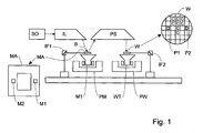
- Figure 1 schematically depicts a lithographic apparatus according to one embodiment of the invention.
- the apparatus comprises:
- the illumination system may include various types of optical components, such as refractive, reflective, magnetic, electromagnetic, electrostatic or other types of optical components, or any combination thereof, for directing, shaping, or controlling radiation.
- optical components such as refractive, reflective, magnetic, electromagnetic, electrostatic or other types of optical components, or any combination thereof, for directing, shaping, or controlling radiation.
- the support structure supports, i.e. bears the weight of, the patterning device. It holds the patterning device in a manner that depends on the orientation of the patterning device, the design of the lithographic apparatus, and other conditions, such as for example whether or not the patterning device is held in a vacuum environment.
- the support structure can use mechanical, vacuum, electrostatic or other clamping techniques to hold the patterning device.
- the support structure may be a frame or a table, for example, which may be fixed or movable as required.
- the support structure may ensure that the patterning device is at a desired position, for example with respect to the projection system. Any use of the terms "reticle” or “mask” herein may be considered synonymous with the more general term "patterning device.”
- patterning device used herein should be broadly interpreted as referring to any device that can be used to impart a radiation beam with a pattern in its cross-section such as to create a pattern in a target portion of the substrate. It should be noted that the pattern imparted to the radiation beam may not exactly correspond to the desired pattern in the target portion of the substrate, for example if the pattern includes phase-shifting features or so called assist features. Generally, the pattern imparted to the radiation beam will correspond to a particular functional layer in a device being created in the target portion, such as an integrated circuit.
- the patterning device may be transmissive or reflective.
- Examples of patterning devices include masks, programmable mirror arrays, and programmable LCD panels.
- Masks are well known in lithography, and include mask types such as binary, alternating phase-shift, and attenuated phase-shift, as well as various hybrid mask types.
- An example of a programmable mirror array employs a matrix arrangement of small mirrors, each of which can be individually tilted so as to reflect an incoming radiation beam in different directions. The tilted mirrors impart a pattern in a radiation beam which is reflected by the mirror matrix.
- projection system used herein should be broadly interpreted as encompassing any type of projection system, including refractive, reflective, catadioptric, magnetic, electromagnetic and electrostatic optical systems, or any combination thereof, as appropriate for the exposure radiation being used, or for other factors such as the use of an immersion liquid or the use of a vacuum. Any use of the term “projection lens” herein may be considered as synonymous with the more general term “projection system”.
- the apparatus is of a reflective type (e.g. employing a reflective mask).
- the apparatus may be of a transmissive type (e.g. employing a transmissive mask).
- the lithographic apparatus may be of a type having two (dual stage) or more substrate tables (and/or two or more mask tables). In such "multiple stage” machines the additional tables may be used in parallel, or preparatory steps may be carried out on one or more tables while one or more other tables are being used for exposure.
- the lithographic apparatus may also be of a type wherein at least a portion of the substrate may be covered by a liquid having a relatively high refractive index, e.g. water, so as to fill a space between the projection system and the substrate.
- a liquid having a relatively high refractive index e.g. water
- An immersion liquid may also be applied to other spaces in the lithographic apparatus, for example, between the mask and the projection system. Immersion techniques are well known in the art for increasing the numerical aperture of projection systems.
- immersion as used herein does not mean that a structure, such as a substrate, must be submerged in liquid, but rather only means that liquid is located between the projection system and the substrate during exposure.
- the illuminator IL receives a radiation beam from a radiation source SO.
- the source and the lithographic apparatus may be separate entities, for example when the source is an excimer laser. In such cases, the source is not considered to form part of the lithographic apparatus and the radiation beam is passed from the source SO to the illuminator IL with the aid of a beam delivery system BD comprising, for example, suitable directing mirrors and/or a beam expander. In other cases the source may be an integral part of the lithographic apparatus, for example when the source is a mercury lamp.
- the source SO and the illuminator IL, together with the beam delivery system BD if required, may be referred to as a radiation system.
- the illuminator IL may comprise an adjuster AD for adjusting the angular intensity distribution of the radiation beam.
- an adjuster AD for adjusting the angular intensity distribution of the radiation beam.
- the illuminator IL may comprise various other components, such as an integrator IN and a condenser CO.
- the illuminator may be used to condition the radiation beam, to have a desired uniformity and intensity distribution in its cross-section.
- the radiation beam B is incident on the patterning device (e.g., mask MA), which is held on the support structure (e.g., mask table MT), and is patterned by the patterning device. Having traversed the mask MA, the radiation beam B passes through the projection system PS, which focuses the beam onto a target portion C of the substrate W.
- the substrate table WT can be moved accurately, e.g. so as to position different target portions C in the path of the radiation beam B.
- the first positioner PM and another position sensor IF1 can be used to accurately position the mask MA with respect to the path of the radiation beam B, e.g. after mechanical retrieval from a mask library, or during a scan.
- movement of the mask table MT may be realized with the aid of a long-stroke module (coarse positioning) and a short-stroke module (fine positioning), which form part of the first positioner PM.
- movement of the substrate table WT may be realized using a long-stroke module and a short-stroke module, which form part of the second positioner PW.
- the mask table MT may be connected to a short-stroke actuator only, or may be fixed.
- Mask MA and substrate W may be aligned using mask alignment marks M1, M2 and substrate alignment marks P1, P2.
- the substrate alignment marks as illustrated occupy dedicated target portions, they may be located in spaces between target portions (these are known as scribe-lane alignment marks).
- the mask alignment marks may be located between the dies.
- the depicted apparatus could be used in at least one of the following modes:
- the present invention may be applied to any component in a lithographic apparatus but is particularly advantageous when applied to optical elements in the path of the projection beam, especially those which become heated by the projection beam, especially mirrors in an EUV lithographic apparatus, especially those of the projection system, where surface deformations have the greatest effect on imaging quality, and those in the beginning of the of the illumination system, where the projection beam intensity is highest, leading to larger temperature variations.
- the present invention is also particular applicable to small mirrors where the thermal load is concentrated, again leading to larger temperature variations.
- the component depicted is a mirror in a reflective lithographic apparatus.
- the invention is not limited in this respect, and it will be understood that the component may also be a lens or other optical element in a transmissive lithographic apparatus.
- the present invention has application during fabrication and/or testing of components during manufacture and maintenance.
- the substantially constant temperature is a mean operating temperature of the lithographic apparatus.
- the component can be tested during fabrication to produce and/or measure the component's behavior at operational temperature.
- the results of the testing may be used to determine an optimal temperature setting in the exposure unit using a thermal tuning algorithm to determine the temperature which results in the lowest optical distortions.
- the component comprises an optical element disposed in a frame in at least one of the illumination system and projection system.
- Figure 2 depicts a component according to an embodiment of the invention.
- figure 2 depicts an optical element 1 for use in a lithographic apparatus.
- the optical element 1 is a mirror for use in a lithographic apparatus operating in the EUV region.
- the mirror is provided with an electrical heating element 2 and a temperature sensor 3, wherein in response to a temperature sensed by the temperature sensor 3, the heating element 2 is arranged to maintain the optical element 1 at a substantially constant predetermined temperature.
- the heating element 2 comprises an electrical heater, for example, a coil.
- the heating element 2 is provided with a power supply and heating element control unit, which are described in more detail with reference to figure 4.
- the heating element 2 provides direct heating to the mirror 1.
- the mirror 1 is disposed in at least one of the illumination system IL and the projection system PS, where in use, it is subject to a thermal load caused by the projection beam and patterned beam PB, respectively.
- the mirror 1 may be disposed in a frame 4.
- the beam PB is incident at a location 7 on a surface of the mirror 1.
- the thermal load caused by the incident beam PB is distributed throughout the mirror 1. However, the majority of the thermal load is distributed in a volume of the mirror 1 located in the vicinity of the location of incidence 7.
- the heating element 2 is controlled to heat the mirror 1 so that the temperature of the mirror 1 is substantially constant.
- the temperature sensor 3 is disposed in the thermal centre of the heating element 2.
- the heating element 2 may be a resistant wire, or an electrical coil.
- the resistant wire may be made of materials such as constantan, which is a copper-nickel alloy with a high electrical resistance and a low temperature coefficient.
- the heating element 3 is provided in a channel 6 formed in the mirror 1.
- the channel 6 extends within the volume of the mirror 1.
- the orientation of the heating element 2 will depend on factors such as the particular thermal load for a particular thermal component and the distribution of the thermal load in the component.
- the thermal load to which the component is subjected may be determined using a thermal analysis, such as a FEM analysis.
- the optimum temperature distribution by the electrical heating elements depends on various factors including the material characteristics of the component, in particular, the coefficient of thermal expansion (CTE) of the component and also the distribution of the dose of the projection beam or patterned beam PB on the component, and furthermore the thermal characteristics of the optical element (e.g. thermal conductivity, heat transfer to environment and heat capacity).
- the mirror may be made of a material having a low CTE, for example, Zerodur (Trademark), which has an extremely low CTE of approximately, 5 ⁇ 10 -9 K -1 .
- the FEM analysis establishes a non-uniform material model of the component, from which the distribution of the thermal load on the component can be established.
- the channel 6 is formed in a bulk of the material of the mirror 1 in the vicinity of the incidence area 7 of the radiation or patterned radiation beam, respectively.
- the channel extends within the bulk material in a direction corresponding substantially to a circumference of the incidence area 7 of the radiation or patterned radiation beam, respectively.
- the channel is disposed in the body of the mirror 1 just below the optical plane where the radiation or patterned radiation beam PB is incident on the surface of the mirror 1.
- the channel 6 extends so that it corresponds to the shape of the cross section of the radiation or patterned radiation (projection) beam PB at the incidence area 7.
- the channel 6 is constructed so that it extends in a manner corresponding to the symmetry of the incident beam PB.
- the channel 6 may be drilled or machined in the mirror, or by means of any other suitable method.
- the heating element 2 is inserted into the channel 6.
- the opening formed in the mirror by the channel 6 may then be closed with a material having a similar or same CTE as the mirror material, for example, Zerodur.
- the heating element 2 may be attached to an outer or underside of the mirror 1 by glueing or other appropriate means.
- the temperature sensor 3 may be mounted in a similar manner to the heating element 2.
- a channel 6' may be formed in the mirror 1.
- the channel 6' is constructed to extend from an outer side of the mirror 1 to the thermal centre of the heating element 2 with which the temperature sensor 3 is associated.
- the leads 8, 9 from the heating element 2 and temperature sensor 3, respectively, are connected to a heating element control means as further described with reference to figure 4.
- the temperature sensor 3 is preferably a high resolution sensor, such as a negative temperature coefficient (NTC) sensor.
- NTC negative temperature coefficient
- it may be a platinum sensor, such as a PT500 or a thermocouple.
- Figure 3 depicts a component according to a further embodiment of the invention.
- figure 3 depicts an example of a mirror 1 suitable for use in a lithographic apparatus operating at an EUV wavelength comprising three independently controlled heating elements 2a, 2b, 2c wherein each heating element 2a, 2b, 2c is associated with a corresponding temperature sensor 3a, 3b, 3c, respectively.
- each heating element 2a, 2b, 2c can be controlled independently from each other.
- heating elements 2a, 2b, 2c Whilst the example in figure 3 shows a plurality of heating elements 2a, 2b, 2c disposed in substantially parallel planes, the invention is not limited in this respect.
- the particular arrangement of the plurality of heating elements may be determined on the basis of the thermal analysis.
- heating elements may be disposed around the edge of the circumference of the mirror in planes substantially orthogonal to the optical plane of the incident beam PB.
- a plurality of temperature sensors 3a, 3b, 3b are provided, wherein each temperature sensor is disposed in the vicinity of one of the plurality of heating elements.
- the temperature sensors 3a, 3b, 3c are disposed at the thermal centre of their respective heating element 2a, 2b, 2c, so that the plurality of heating elements are controllable independently of each other, in response to the respective temperatures sensed by the plurality of temperature sensors 3a, 3b, 3c disposed in the vicinity of the respective heating elements.
- a heater supply control means 44 controls the voltage V1, V2, V3, respectively, applied to the resistance wire of the heating elements 2a, 2b, 2c, respectively.
- Figure 4 depicts details of a lithographic apparatus including a component mounted in a frame according to an embodiment of the invention.
- FIG 4 depicts a projection system PS.
- the projection system PS comprises a frame 4, otherwise referred to in the art as a projection optics assembly, which supports a plurality of mirrors M1-M6 that are disposed in a spaced relationship.
- the frame 4 is provided with an opening 5 through which the patterned beam PB enters the assembly.
- the frame 4 may be provided with a further opening 5' through which the heating element control means 44 is connectable with the heating element 2. In this way, the control of the heating elements 2 may be carried out remotely.
- the patterned beam PB is incident on the plurality of optical elements, shown as mirrors M1-M6 is a predetermined order.
- the patterned beam PB is incident on the mirrors M1-M6, in the order M1, M2, M3, M4, M5 and M6, wherein M1 is the first mirror and M6 is the last mirror. Having been reflected by the last mirror M6, the patterned beam PB is incident on the substrate W. It has been found that the higher the mirror is in the incidence order the greater thermal load it receives in use from the patterned beam PB. Thus, the first mirror M1 receives a higher thermal load than M2. The second mirror M2 receives a higher thermal load than M3, etc.
- the temperatures of the mirrors M1-M6 can be controlled to be substantially constant with respect to each other and the predetermined temperature.
- mirror M1 may be provided with four heating elements provided in an arrangement in accordance with the distribution of the thermal load
- the last mirror M6 may only require one or two or even no heating elements.
- a plurality of the optical elements are provided with at least one of the heating elements, wherein the number of heating elements provided for each respective optical element is determined in accordance with the thermal load to which each of the optical elements is subjected to in combination with the sensitivity for optical aberration of this optical component with respect to this thermal load.
- first optical element M1 on which at least one of the projection beam and patterned beam is incident first is provided with a number of heating elements exceeding the number of heating elements provided with at least one of the optical elements M2, M3, M4, M5, M6 disposed downstream of the first optical element in the direction of the propagation of the at least projection beam and patterned beam.
- the temperature of the mirrors is more accurately controlled.
- the first mirror M1 is the most critical since it receives the largest thermal load.
- other components such as smaller components also receive a relatively large thermal load and may require larger number of heating elements than other components, the same can be stated for very sensitive optical components in the optical system.
- figure 4 shows a first mirror M1 provided with a heating element 2 and a temperature sensor 3, this is a schematic representation and not intended to limit the invention. As described above, at least one of the mirrors may be provided with at least one or more heating elements in accordance with the thermal load each mirror bears with respect to the other mirrors. Figure 4 depicts only one heating element by way of example, only.
- the apparatus further comprises a power supply 40 and a heating element control means 44 for controlling the heating element 2 in response to the temperature measured by the temperature sensor 3.
- the heating element control means 44 is arranged to control the voltage supplied by the power supply 40 to the heating element 2. If so desired, the heating element control means 44 may control the power supply 40 to control the voltage supplied by the or more than one power supplies (not shown) to a plurality of heating elements.
- the heating element control means 44 is depicted as forming a component of the power supply 40. However, in an alternative embodiment, the heating element control means 44 may be provided remotely from the power supply or power supplies, if there is a plurality of power supplies (not shown).
- the heating elements are controlled so that they are maintained at a predetermined temperature.
- the control may be carried out using proportional and differential (PID) control but also other control algorithms can be used.
- PID proportional and differential
- the predetermined temperature will vary depending on the particular application of the present invention. For example, when a lithographic apparatus is first switched on the temperature of the apparatus is relatively low, for example, 22 degrees Celsius. Whilst the apparatus is running its temperature rises to a steady state temperature of, for example, 35 degrees Celsius.
- the heating element or elements are controlled so that they are constantly at a steady state.
- the heating element control means will cause the heating elements to heat up to the predetermined temperature.
- the heating element control means 44 is arranged in response to the temperatures measured by the temperature sensors to maintain the components at the predetermined temperature. Because, the components are brought into a steady state, that is for example, at a temperature slightly higher than the steady state of the lithographic apparatus, as the lithographic apparatus is in use, the temperature of the optical elements does not rise higher than the predetermined temperature.
- the substantially constant temperature is a mean operating temperature of the lithographic apparatus.
- the behavior of the component may be analyzed as if it were in situ in the apparatus.
- lithographic apparatus in the manufacture of ICs
- the lithographic apparatus described herein may have other applications, such as the manufacture of integrated optical systems, guidance and detection patterns for magnetic domain memories, flat-panel displays, liquid-crystal displays (LCDs), thin-film magnetic heads, etc.
- LCDs liquid-crystal displays
- any use of the terms “wafer” or “die” herein may be considered as synonymous with the more general terms “substrate” or "target portion”, respectively.
- the substrate referred to herein may be processed, before or after exposure, in for example a track (a tool that typically applies a layer of resist to a substrate and develops the exposed resist), a metrology tool and/or an inspection tool. Where applicable, the disclosure herein may be applied to such and other substrate processing tools. Further, the substrate may be processed more than once, for example in order to create a multi-layer IC, so that the term substrate used herein may also refer to a substrate that already contains multiple processed layers.
- imprint lithography a topography in a patterning device defines the pattern created on a substrate.
- the topography of the patterning device may be pressed into a layer of resist supplied to the substrate whereupon the resist is cured by applying electromagnetic radiation, heat, pressure or a combination thereof.
- the patterning device is moved out of the resist leaving a pattern in it after the resist is cured.
- UV radiation e.g. having a wavelength of or about 365, 355, 248, 193, 157 or 126 nm
- EUV radiation e.g. having a wavelength in the range of 5-20 nm
- particle beams such as ion beams or electron beams.
- lens may refer to any one or combination of various types of optical components, including refractive, reflective, magnetic, electromagnetic and electrostatic optical components.
- the invention may take the form of a computer program containing one or more sequences of machine-readable instructions describing a method as disclosed above, or a data storage medium (e.g. semiconductor memory, magnetic or optical disk) having such a computer program stored therein.
- a data storage medium e.g. semiconductor memory, magnetic or optical disk
Applications Claiming Priority (1)
| Application Number | Priority Date | Filing Date | Title |
|---|---|---|---|
| US10/910,792 US7375794B2 (en) | 2004-08-04 | 2004-08-04 | Lithographic apparatus and device manufacturing method |
Publications (3)
| Publication Number | Publication Date |
|---|---|
| EP1624342A2 true EP1624342A2 (de) | 2006-02-08 |
| EP1624342A3 EP1624342A3 (de) | 2009-09-23 |
| EP1624342B1 EP1624342B1 (de) | 2011-07-06 |
Family
ID=35355401
Family Applications (1)
| Application Number | Title | Priority Date | Filing Date |
|---|---|---|---|
| EP05076746A Expired - Fee Related EP1624342B1 (de) | 2004-08-04 | 2005-07-28 | Lithographischer Apparat, optisches Element für einen lithographischen Apparat und Verfahren zur Herstellung einer Vorrichtung |
Country Status (7)
| Country | Link |
|---|---|
| US (1) | US7375794B2 (de) |
| EP (1) | EP1624342B1 (de) |
| JP (2) | JP4495046B2 (de) |
| KR (1) | KR100697297B1 (de) |
| CN (1) | CN1734354A (de) |
| SG (1) | SG119304A1 (de) |
| TW (1) | TWI284359B (de) |
Families Citing this family (20)
| Publication number | Priority date | Publication date | Assignee | Title |
|---|---|---|---|---|
| DE102006021797A1 (de) | 2006-05-09 | 2007-11-15 | Carl Zeiss Smt Ag | Optische Abbildungseinrichtung mit thermischer Dämpfung |
| US20080049202A1 (en) * | 2006-08-22 | 2008-02-28 | Carl Zeiss Smt Ag | Projection exposure apparatus for semiconductor lithography |
| IL181500A0 (en) * | 2007-02-22 | 2007-07-04 | Belkin Lev | Scale inhibiting heating device |
| US8064151B2 (en) * | 2007-08-14 | 2011-11-22 | Asml Netherlands B.V. | Lithographic apparatus and thermal optical manipulator control method |
| KR101670518B1 (ko) * | 2007-10-09 | 2016-10-28 | 칼 짜이스 에스엠테 게엠베하 | 광학 소자의 온도 제어 장치 |
| US7960701B2 (en) | 2007-12-20 | 2011-06-14 | Cymer, Inc. | EUV light source components and methods for producing, using and refurbishing same |
| NL2003341A (en) * | 2008-08-22 | 2010-03-10 | Asml Netherlands Bv | Lithographic apparatus and device manufacturing method. |
| US7641349B1 (en) | 2008-09-22 | 2010-01-05 | Cymer, Inc. | Systems and methods for collector mirror temperature control using direct contact heat transfer |
| EP2396794A1 (de) | 2009-02-13 | 2011-12-21 | ASML Netherlands BV | Mehrschichtiger spiegel und lithographievorrichtung |
| CN101609262B (zh) * | 2009-07-14 | 2011-08-10 | 上海微电子装备有限公司 | 光刻机投影物镜的温度控制装置 |
| NL2005449A (en) * | 2009-11-16 | 2012-04-05 | Asml Netherlands Bv | Lithographic method and apparatus. |
| CN102375344B (zh) * | 2010-08-18 | 2013-09-11 | 上海微电子装备有限公司 | 控制透镜像质变化的方法 |
| JP5739182B2 (ja) | 2011-02-04 | 2015-06-24 | インターナショナル・ビジネス・マシーンズ・コーポレーションInternational Business Machines Corporation | 制御システム、方法およびプログラム |
| JP5731223B2 (ja) | 2011-02-14 | 2015-06-10 | インターナショナル・ビジネス・マシーンズ・コーポレーションInternational Business Machines Corporation | 異常検知装置、監視制御システム、異常検知方法、プログラムおよび記録媒体 |
| JP5689333B2 (ja) | 2011-02-15 | 2015-03-25 | インターナショナル・ビジネス・マシーンズ・コーポレーションInternational Business Machines Corporation | 異常検知システム、異常検知装置、異常検知方法、プログラムおよび記録媒体 |
| DE102011077784A1 (de) * | 2011-06-20 | 2012-12-20 | Carl Zeiss Smt Gmbh | Projektionsanordnung |
| US9575415B2 (en) * | 2014-05-22 | 2017-02-21 | Taiwan Semiconductor Manufacturing Company, Ltd. | Wafer stage temperature control |
| DE102014224822A1 (de) * | 2014-12-04 | 2016-06-09 | Carl Zeiss Smt Gmbh | Spiegel für eine lithographieanlage, projektionssystem für eine lithographieanlage und lithographieanlage |
| NL2021342A (en) * | 2017-09-04 | 2019-03-11 | Asml Netherlands Bv | Heating system |
| DE102021200788A1 (de) | 2021-01-28 | 2022-07-28 | Carl Zeiss Smt Gmbh | Optisches System, sowie Verfahren zum Betreiben eines optischen Systems |
Citations (1)
| Publication number | Priority date | Publication date | Assignee | Title |
|---|---|---|---|---|
| EP1376239A2 (de) | 2002-06-25 | 2004-01-02 | Nikon Corporation | Kühlvorrichtung für ein optisches Element |
Family Cites Families (31)
| Publication number | Priority date | Publication date | Assignee | Title |
|---|---|---|---|---|
| DE216231C (de) * | ||||
| JPS6119129A (ja) * | 1984-07-05 | 1986-01-28 | Nippon Kogaku Kk <Nikon> | 投影光学装置 |
| JP3132086B2 (ja) * | 1991-09-07 | 2001-02-05 | キヤノン株式会社 | 光学素子の形状制御方法および露光装置 |
| EP0532236B1 (de) * | 1991-09-07 | 1997-07-16 | Canon Kabushiki Kaisha | System zur Stabilisierung der Formen von optischen Elementen, Belichtungsvorrichtung unter Verwendung dieses Systems und Verfahren zur Herstellung von Halbleitervorrichtungen |
| JPH05291117A (ja) | 1992-04-14 | 1993-11-05 | Hitachi Ltd | 投影露光方法およびその装置 |
| JP3144069B2 (ja) * | 1992-06-12 | 2001-03-07 | キヤノン株式会社 | 投影露光装置及びそれを用いた半導体素子の製造方法 |
| JP3309867B2 (ja) | 1993-01-06 | 2002-07-29 | 株式会社ニコン | 露光装置及び照明光学装置 |
| JP3368091B2 (ja) * | 1994-04-22 | 2003-01-20 | キヤノン株式会社 | 投影露光装置及びデバイスの製造方法 |
| JPH0845827A (ja) * | 1994-07-28 | 1996-02-16 | Canon Inc | 投影露光装置及びそれを用いた半導体デバイスの製造方法 |
| US5774274A (en) * | 1995-05-12 | 1998-06-30 | Schachar; Ronald A. | Variable focus lens by small changes of the equatorial lens diameter |
| US5883704A (en) * | 1995-08-07 | 1999-03-16 | Nikon Corporation | Projection exposure apparatus wherein focusing of the apparatus is changed by controlling the temperature of a lens element of the projection optical system |
| JPH09232213A (ja) * | 1996-02-26 | 1997-09-05 | Nikon Corp | 投影露光装置 |
| JP3360282B2 (ja) * | 1997-06-19 | 2002-12-24 | 住友重機械工業株式会社 | 微細構造体の製造方法 |
| DE19752713A1 (de) * | 1997-11-28 | 1999-06-02 | Zeiss Carl Fa | UV-Optisches System mit reduzierter Alterung |
| JP2000036449A (ja) * | 1998-07-17 | 2000-02-02 | Nikon Corp | 露光装置 |
| JP2000143278A (ja) * | 1998-11-10 | 2000-05-23 | Nikon Corp | 耐久性の向上された投影露光装置及び結像光学系の製造方法 |
| US6098408A (en) | 1998-11-11 | 2000-08-08 | Advanced Micro Devices | System for controlling reflection reticle temperature in microlithography |
| JP3862438B2 (ja) * | 1998-12-28 | 2006-12-27 | キヤノン株式会社 | 走査露光装置、走査露光方法およびデバイス製造方法 |
| US6882477B1 (en) * | 1999-11-10 | 2005-04-19 | Massachusetts Institute Of Technology | Method and system for interference lithography utilizing phase-locked scanning beams |
| DE19956353C1 (de) * | 1999-11-24 | 2001-08-09 | Zeiss Carl | Optische Anordnung |
| US6445439B1 (en) * | 1999-12-27 | 2002-09-03 | Svg Lithography Systems, Inc. | EUV reticle thermal management |
| JP4634581B2 (ja) * | 2000-07-06 | 2011-02-16 | キヤノンアネルバ株式会社 | スパッタリング方法、表面処理方法、スパッタリング装置及び表面処理装置 |
| US6630984B2 (en) | 2000-08-03 | 2003-10-07 | Asml Netherlands B.V. | Lithographic apparatus, device manufacturing method, and device manufactured thereby |
| DE10040998A1 (de) * | 2000-08-22 | 2002-03-14 | Zeiss Carl | Projektionsbelichtungsanlage |
| DE10050125A1 (de) * | 2000-10-11 | 2002-04-25 | Zeiss Carl | Vorrichtung zum Temperaturausgleich für thermisch belastete Körper mit niederer Wärmeleitfähigkeit, insbesondere für Träger reflektierender Schichten oder Substrate in der Optik |
| JP2002313890A (ja) * | 2001-04-11 | 2002-10-25 | Sumitomo Electric Ind Ltd | 被加熱物搭載用ヒータ部材およびそれを用いた基板処理装置 |
| JP3422991B2 (ja) | 2001-05-28 | 2003-07-07 | 株式会社東芝 | 荷電粒子描画装置 |
| US6994444B2 (en) | 2002-06-14 | 2006-02-07 | Asml Holding N.V. | Method and apparatus for managing actinic intensity transients in a lithography mirror |
| US7132206B2 (en) * | 2002-09-17 | 2006-11-07 | International Business Machines Corporation | Process and apparatus for minimizing thermal gradients across an advanced lithographic mask |
| JP2004111684A (ja) | 2002-09-19 | 2004-04-08 | Nikon Corp | ステージ装置及び露光装置 |
| US20040252287A1 (en) * | 2003-06-11 | 2004-12-16 | Michael Binnard | Reaction frame assembly that functions as a reaction mass |
-
2004
- 2004-08-04 US US10/910,792 patent/US7375794B2/en active Active
-
2005
- 2005-07-11 SG SG200504355A patent/SG119304A1/en unknown
- 2005-07-22 TW TW094125027A patent/TWI284359B/zh not_active IP Right Cessation
- 2005-07-28 EP EP05076746A patent/EP1624342B1/de not_active Expired - Fee Related
- 2005-08-03 JP JP2005224791A patent/JP4495046B2/ja not_active Expired - Fee Related
- 2005-08-03 CN CNA200510091134XA patent/CN1734354A/zh active Pending
- 2005-08-04 KR KR1020050071177A patent/KR100697297B1/ko active IP Right Grant
-
2009
- 2009-08-17 JP JP2009188270A patent/JP5155967B2/ja not_active Expired - Fee Related
Patent Citations (1)
| Publication number | Priority date | Publication date | Assignee | Title |
|---|---|---|---|---|
| EP1376239A2 (de) | 2002-06-25 | 2004-01-02 | Nikon Corporation | Kühlvorrichtung für ein optisches Element |
Also Published As
| Publication number | Publication date |
|---|---|
| KR20060049272A (ko) | 2006-05-18 |
| US20060028627A1 (en) | 2006-02-09 |
| JP5155967B2 (ja) | 2013-03-06 |
| EP1624342B1 (de) | 2011-07-06 |
| TW200619860A (en) | 2006-06-16 |
| KR100697297B1 (ko) | 2007-03-20 |
| SG119304A1 (en) | 2006-02-28 |
| JP2009272649A (ja) | 2009-11-19 |
| JP2006049909A (ja) | 2006-02-16 |
| TWI284359B (en) | 2007-07-21 |
| EP1624342A3 (de) | 2009-09-23 |
| CN1734354A (zh) | 2006-02-15 |
| JP4495046B2 (ja) | 2010-06-30 |
| US7375794B2 (en) | 2008-05-20 |
Similar Documents
| Publication | Publication Date | Title |
|---|---|---|
| EP1624342B1 (de) | Lithographischer Apparat, optisches Element für einen lithographischen Apparat und Verfahren zur Herstellung einer Vorrichtung | |
| EP1921505B1 (de) | Lithographischer Apparat und Verfahren zur Herstellung einer Vorrichtung | |
| KR101619280B1 (ko) | 투영 시스템 및 리소그래피 장치 | |
| US7359029B2 (en) | Lithographic apparatus and method of reducing thermal distortion | |
| EP1653283A2 (de) | Lithographischer Apparat und Verfahren zur Herstellung einer Vorrichtung | |
| US9482967B2 (en) | Lithographic apparatus, control system and device manufacturing method | |
| US8879044B2 (en) | Lithographic apparatus, and motor cooling device | |
| KR20140140541A (ko) | 기판 테이블의 위치를 측정하기 위한 메트롤로지 시스템을 갖는 리소그래피 장치 | |
| US7746447B2 (en) | Lithographic apparatus, device manufacturing method and method of calibrating a lithographic apparatus | |
| US7170582B2 (en) | Support device and lightographic apparatus | |
| US7379156B2 (en) | Lithographic apparatus and device manufacturing method | |
| EP1498781B1 (de) | Lithografisches Immersionsgerät und Verfahren zur Herstellung einer Vorrichtung | |
| US20060017906A1 (en) | Lithographic apparatus and device manufacturing method | |
| US11835106B2 (en) | Method for manufacturing damper device, lithographic apparatus, projection system, and device manufacturing method | |
| KR20200094206A (ko) | 리소그래피 장치, 동작 방법 및 디바이스 제조 방법 |
Legal Events
| Date | Code | Title | Description |
|---|---|---|---|
| PUAI | Public reference made under article 153(3) epc to a published international application that has entered the european phase |
Free format text: ORIGINAL CODE: 0009012 |
|
| AK | Designated contracting states |
Kind code of ref document: A2 Designated state(s): AT BE BG CH CY CZ DE DK EE ES FI FR GB GR HU IE IS IT LI LT LU LV MC NL PL PT RO SE SI SK TR |
|
| AX | Request for extension of the european patent |
Extension state: AL BA HR MK YU |
|
| PUAL | Search report despatched |
Free format text: ORIGINAL CODE: 0009013 |
|
| AK | Designated contracting states |
Kind code of ref document: A3 Designated state(s): AT BE BG CH CY CZ DE DK EE ES FI FR GB GR HU IE IS IT LI LT LU LV MC NL PL PT RO SE SI SK TR |
|
| AX | Request for extension of the european patent |
Extension state: AL BA HR MK YU |
|
| AKX | Designation fees paid | ||
| 17P | Request for examination filed |
Effective date: 20091009 |
|
| RBV | Designated contracting states (corrected) |
Designated state(s): DE FR |
|
| 17Q | First examination report despatched |
Effective date: 20100601 |
|
| REG | Reference to a national code |
Ref country code: DE Ref legal event code: 8566 |
|
| GRAP | Despatch of communication of intention to grant a patent |
Free format text: ORIGINAL CODE: EPIDOSNIGR1 |
|
| RTI1 | Title (correction) |
Free format text: LITHOGRAPHIC APPARATUS, OPTICAL ELEMENT FOR A LITHOGRAPHIC APPARATUS AND DEVICE MANUFACTURING METHOD |
|
| GRAS | Grant fee paid |
Free format text: ORIGINAL CODE: EPIDOSNIGR3 |
|
| GRAA | (expected) grant |
Free format text: ORIGINAL CODE: 0009210 |
|
| AK | Designated contracting states |
Kind code of ref document: B1 Designated state(s): DE FR |
|
| REG | Reference to a national code |
Ref country code: DE Ref legal event code: R096 Ref document number: 602005028830 Country of ref document: DE Effective date: 20110825 |
|
| PLBE | No opposition filed within time limit |
Free format text: ORIGINAL CODE: 0009261 |
|
| STAA | Information on the status of an ep patent application or granted ep patent |
Free format text: STATUS: NO OPPOSITION FILED WITHIN TIME LIMIT |
|
| 26N | No opposition filed |
Effective date: 20120411 |
|
| REG | Reference to a national code |
Ref country code: DE Ref legal event code: R097 Ref document number: 602005028830 Country of ref document: DE Effective date: 20120411 |
|
| REG | Reference to a national code |
Ref country code: FR Ref legal event code: PLFP Year of fee payment: 12 |
|
| REG | Reference to a national code |
Ref country code: FR Ref legal event code: PLFP Year of fee payment: 13 |
|
| REG | Reference to a national code |
Ref country code: FR Ref legal event code: PLFP Year of fee payment: 14 |
|
| PGFP | Annual fee paid to national office [announced via postgrant information from national office to epo] |
Ref country code: FR Payment date: 20180725 Year of fee payment: 14 |
|
| PG25 | Lapsed in a contracting state [announced via postgrant information from national office to epo] |
Ref country code: FR Free format text: LAPSE BECAUSE OF NON-PAYMENT OF DUE FEES Effective date: 20190731 |
|
| PGFP | Annual fee paid to national office [announced via postgrant information from national office to epo] |
Ref country code: DE Payment date: 20200721 Year of fee payment: 16 |
|
| REG | Reference to a national code |
Ref country code: DE Ref legal event code: R119 Ref document number: 602005028830 Country of ref document: DE |
|
| PG25 | Lapsed in a contracting state [announced via postgrant information from national office to epo] |
Ref country code: DE Free format text: LAPSE BECAUSE OF NON-PAYMENT OF DUE FEES Effective date: 20220201 |