EP1624332B1 - Dünnfilmtransistorpanel und eine Flüssigkristallanzeige - Google Patents
Dünnfilmtransistorpanel und eine Flüssigkristallanzeige Download PDFInfo
- Publication number
- EP1624332B1 EP1624332B1 EP05107132A EP05107132A EP1624332B1 EP 1624332 B1 EP1624332 B1 EP 1624332B1 EP 05107132 A EP05107132 A EP 05107132A EP 05107132 A EP05107132 A EP 05107132A EP 1624332 B1 EP1624332 B1 EP 1624332B1
- Authority
- EP
- European Patent Office
- Prior art keywords
- pixel
- sub
- pixel electrode
- electrode
- electrodes
- Prior art date
- Legal status (The legal status is an assumption and is not a legal conclusion. Google has not performed a legal analysis and makes no representation as to the accuracy of the status listed.)
- Not-in-force
Links
Images


Classifications
-
- G—PHYSICS
- G02—OPTICS
- G02F—OPTICAL DEVICES OR ARRANGEMENTS FOR THE CONTROL OF LIGHT BY MODIFICATION OF THE OPTICAL PROPERTIES OF THE MEDIA OF THE ELEMENTS INVOLVED THEREIN; NON-LINEAR OPTICS; FREQUENCY-CHANGING OF LIGHT; OPTICAL LOGIC ELEMENTS; OPTICAL ANALOGUE/DIGITAL CONVERTERS
- G02F1/00—Devices or arrangements for the control of the intensity, colour, phase, polarisation or direction of light arriving from an independent light source, e.g. switching, gating or modulating; Non-linear optics
- G02F1/01—Devices or arrangements for the control of the intensity, colour, phase, polarisation or direction of light arriving from an independent light source, e.g. switching, gating or modulating; Non-linear optics for the control of the intensity, phase, polarisation or colour
- G02F1/13—Devices or arrangements for the control of the intensity, colour, phase, polarisation or direction of light arriving from an independent light source, e.g. switching, gating or modulating; Non-linear optics for the control of the intensity, phase, polarisation or colour based on liquid crystals, e.g. single liquid crystal display cells
- G02F1/133—Constructional arrangements; Operation of liquid crystal cells; Circuit arrangements
- G02F1/1333—Constructional arrangements; Manufacturing methods
- G02F1/1343—Electrodes
- G02F1/134309—Electrodes characterised by their geometrical arrangement
- G02F1/134336—Matrix
-
- G—PHYSICS
- G02—OPTICS
- G02F—OPTICAL DEVICES OR ARRANGEMENTS FOR THE CONTROL OF LIGHT BY MODIFICATION OF THE OPTICAL PROPERTIES OF THE MEDIA OF THE ELEMENTS INVOLVED THEREIN; NON-LINEAR OPTICS; FREQUENCY-CHANGING OF LIGHT; OPTICAL LOGIC ELEMENTS; OPTICAL ANALOGUE/DIGITAL CONVERTERS
- G02F1/00—Devices or arrangements for the control of the intensity, colour, phase, polarisation or direction of light arriving from an independent light source, e.g. switching, gating or modulating; Non-linear optics
- G02F1/01—Devices or arrangements for the control of the intensity, colour, phase, polarisation or direction of light arriving from an independent light source, e.g. switching, gating or modulating; Non-linear optics for the control of the intensity, phase, polarisation or colour
- G02F1/13—Devices or arrangements for the control of the intensity, colour, phase, polarisation or direction of light arriving from an independent light source, e.g. switching, gating or modulating; Non-linear optics for the control of the intensity, phase, polarisation or colour based on liquid crystals, e.g. single liquid crystal display cells
- G02F1/133—Constructional arrangements; Operation of liquid crystal cells; Circuit arrangements
- G02F1/136—Liquid crystal cells structurally associated with a semi-conducting layer or substrate, e.g. cells forming part of an integrated circuit
- G02F1/1362—Active matrix addressed cells
- G02F1/136213—Storage capacitors associated with the pixel electrode
-
- G—PHYSICS
- G02—OPTICS
- G02F—OPTICAL DEVICES OR ARRANGEMENTS FOR THE CONTROL OF LIGHT BY MODIFICATION OF THE OPTICAL PROPERTIES OF THE MEDIA OF THE ELEMENTS INVOLVED THEREIN; NON-LINEAR OPTICS; FREQUENCY-CHANGING OF LIGHT; OPTICAL LOGIC ELEMENTS; OPTICAL ANALOGUE/DIGITAL CONVERTERS
- G02F2201/00—Constructional arrangements not provided for in groups G02F1/00 - G02F7/00
- G02F2201/52—RGB geometrical arrangements
Definitions
- the present invention relates to a liquid crystal display and a thin film transistor array panel.
- a liquid crystal display is a common type of flat panel display.
- An LCD includes two panels provided with field-generating electrodes, and a liquid crystal (LC) layer interposed therebetween.
- the LCD displays images by applying voltages to the field-generating electrodes to generate an electric field in the LC layer, which changes orientations of LC molecules in the LC layer to adjust polarization of incident light.
- a disadvantage of the LCD is that it has a relatively narrow viewing angle.
- Various techniques for enlarging the viewing angle have been suggested, such as utilizing a vertically aligned LC and providing cutouts or protrusions at field-generating electrodes such as pixel electrodes and a common electrode.
- the cutouts induce a slanted electric field, and the slanted electric field controls falling directions of liquid crystals. Control of the falling direction of liquid crystals makes it possible to widen the viewing angle of liquid crystal display.
- the protrusions are formed on both of pixel electrodes and a common electrode, the protrusions induce a slanted electric field, and the slanted electric field controls falling directions of liquid crystals.
- Additional methods in which pixel electrodes have cutouts and protrusions formed on a common electrode may be used to control falling directions of liquid crystals.
- An LCD using cutouts or protrusions has a viewing angle of greater than approximately 80 degrees in any direction, which has an improved contrast ratio in view of a standard contrast ratio of 1:10, and in view of gray scale inversion where a viewing angle of occurring brightness inversion is a standard angle.
- Such an LCD shows poor visibility that is inferior to a twisted nematic mode LCD. The poor visibility is caused by discordance of the gamma curve between the front view and lateral view.
- JP 09-269 509 A discloses the features of the precharacterizing portions of claims 1 and 6.
- the present invention provides an LCD having a high transmittance ratio and a small difference in color tone between a front view and a lateral view.
- the present invention comprises the features of independent claims 1 and 6.
- Fig. 1 is a layout view of a thin film transistor (TFT) array panel for an LCD according to an embodiment of the invention.
- TFT thin film transistor
- Fig. 2 is a layout view of a color filter panel for an LCD according to an embodiment of the invention.
- Fig. 3 is a layout view of a red pixel of an LCD according to the embodiment shown in Fig. 1 and Fig. 2 .
- Fig. 4 is a sectional view of the LCD shown in Fig. 3 taken along the line IV-IV'.
- Fig. 5 is a circuit diagram of the LCD shown in Figs. 1 , 2 , 3 , and 4 .
- Fig. 6 shows gamma curves relating to an LCD according to an embodiment of the invention.
- Fig. 7 is a layout view of a TFT array panel for an LCD according to another embodiment of the invention.
- Fig. 8 is a sectional view of the TFT array panel shown in Fig. 7 taken along the line VIII-VIII'.
- Fig. 9 is a layout view of a TFT array panel for an LCD according to another embodiment of the invention.
- Fig. 10 is a sectional view of an LCD including the TFT array panel shown in Fig. 9 taken along the line X-X'.
- Fig. 11 is a layout view of a TFT array panel for an LCD according to another embodiment of the invention.
- Fig. 12 is a sectional view of an LCD including the TFT array panel shown in Fig. 11 taken along the line XII-XII'.
- Fig. 1 is a layout view of a thin film transistor (TFT) array panel for an LCD according to an embodiment of the invention.
- Fig. 2 is a layout view of a color filter panel for an LCD according to an embodiment of the invention.
- Fig. 3 is a layout view of a red pixel of an LCD according to the embodiment shown in Fig. 1 and Fig. 2 .
- Fig. 4 is a sectional view of the LCD shown in Fig. 3 taken along the line IV-IV'.
- an LCD includes a TFT array panel 100, a common electrode panel 200, and a LC layer 3 provided between the panels 100 and 200 and including a plurality of LC molecules aligned vertically with respect to surfaces of the panels 100 and 200.
- a structure of the TFT array panel 100 is described below.
- a plurality of first and second pixel electrodes 190a and 190b made of indium tin oxide (ITO) or indium zinc oxide (IZO) may be formed on an insulating substrate 110 made of a transparent material, such as glass.
- the first pixel electrode 190a is connected with a thin film transistor and receives image data voltages.
- the second pixel electrode 190b is overlaps with a coupling electrode 176 that is connected with the first pixel electrode 190a. Therefore, the second pixel electrode 190b is electrically coupled with the first pixel electrode 190a.
- the overlapping areas between the second pixel electrode 190b and the coupling electrode 176 are different among red, green, and blue pixels.
- a polarizer 12 is attached with the lower surface of the insulating substrate 110.
- the first and second pixel electrodes 190a and 190b may be made of a non-transparent material. It is understood that the polarizer 12 may be omitted when necessary.
- a structure of the color filter panel 200 is described below.
- a light blocking layer 220 to prevent light leakage, red, green, and blue color filters 230, and a common electrode 270 made of a transparent conductor, such as ITO or IZO are formed on an insulating substrate 210 made of a transparent material, such as glass.
- the common electrode 270 includes cutouts 271, 272, and 273.
- the light blocking layer 220 may be formed on areas overlapping the cutouts 271, 272, and 273, as well as near pixel areas to prevent light leakage due to the cutouts 271, 272, and 273.
- Alignment layers 11 and 21 are respectively formed on inner surfaces of the two panels 100 and 200 to align liquid crystal molecules.
- the alignment layers I 1 and 21 may vertically align the liquid crystal molecules with respect to the surfaces of the substrates 110 and 210; however, this is not necessary.
- the TFT array panel 100 is described below with reference to Figs. 1 , 4 , and 5 .
- a plurality of gate lines 121 and a plurality of storage electrode lines 131 are formed on an insulating substrate 110.
- the gate lines 121 extend substantially in a transverse direction and each gate line 121 has a plurality of protruding gate electrodes 124, e.g., PROTRUSIONS, protruding along upper and lower side, and an expansion 129 or end portion for connecting to an external circuit.
- the expansion 129 may be wider than other portions of the gate line 121 except for the gate electrodes 124.
- the gate lines 121 transmit gate signals and extend substantially in a transverse direction.
- the expansion 129 of the gate lines 121 has an area that is sufficiently large for contact with another layer or an external driving circuit.
- a gate driving circuit (not shown) for generating the gate signals may be mounted or attached on a flexible printed circuit (FPC) film (not shown).
- the FPC may be attached with the substrate 110, directly mounted on the substrate 110, or integrated onto the substrate 110.
- the gate lines 121 may extend and connect with a driving circuit that may be integrated on the substrate 110.
- Each storage electrode line 1.31 extends substantially in the transverse direction and includes a plurality of sets of storage electrodes 133a, 133b, and 133c. Two storage electrodes 133a and 133b are extended substantially in a longitudinal direction and are connected with a transverse storage electrode 1.33c.
- the storage line 131 may include two or more transverse lines. The storage electrode line 131 may be provided at a substantially center portion of the two adjacent gate lines 121.
- the gate lines 121 and the storage electrode lines 131 may be made of an Al containing metal such as Al and Al alloy, an Ag containing metal such as Ag and Ag alloy, a Cu containing metal such as Cu and Cu alloy, a Mo containing metal such as Mo and Mo alloy, Cr, Ta, or Ti.
- the gate lines 121 may have a multi-layered structure including two conductive films (not shown) having different physical characteristics One of the two films may be made of a low resistivity metal including the Al containing metal, the Ag containing metal, and the Cu containing metal for reducing signal delay or voltage drop.
- the other film may be made of material such as a Mo containing metal, a Cr containing metal, a Ta containing metal, or a Ti containing metal, which have good physical, chemical, and electrical contact characteristics with other materials such as indium tin oxide (ITO) or indium zinc oxide (IZO).
- ITO indium tin oxide
- IZO indium zinc oxide
- the gate lines 121 and the storage electrode lines 131 may be formed of various metal or conductor other than the above described materials.
- the lateral sides of the gate lines 121 and the storage electrode lines 131 are tapered or angled, and the inclination angle of the lateral sides with respect to a surface of the substrate 110 ranges between about 30 to about 80 degrees.
- a gate insulating layer 140 may be made of silicon nitride (SiNx) and is formed on the gate lines 121 and the storage electrode lines 131.
- a plurality of data lines 171, a plurality of drain electrodes 175, and a plurality of under-bridge metal pieces 172 are formed on the gate insulating layer 140.
- Each data line 171 extends substantially in the longitudinal direction and has a plurality of source electrodes 173 extending toward the drain electrodes 175.
- Each data line 171 includes an expansion 179 that may be wider than the data line so that the expansion 179 contacts another layer or an external device.
- the drain electrode 175 may extend to form a coupling electrode 176.
- the coupling electrode 176 may be bent to have a substantially "V" shape.
- the coupling electrodes 176 for the red, green, and blue pixels each have different lengths.
- the length of the coupling electrode 176 in the red (R) pixel may be the longest
- the length of the coupling electrode 176 in the blue (B) pixel may be the second longest
- the length of the coupling electrode 176 in the green (G) pixel may be the shortest.
- the under-bridge metal peaces 172 are disposed on the gate line 121 near the gate electrode 124.
- the data lines 171, drain electrodes 175, and the under-bridge metal pieces 172 may be made of a refractory metal such as Cr, Mo, Ta, Ti, or alloys thereof. However, they may have a multilayered structure including a refractory metal film (not shown) and a low resistivity film made of a metal such as an Al containing metal, an Ag containing metal, and a Cu containing metal.
- a plurality of semiconductor stripes 151 are formed under the data lines 171 and the drain electrodes 175 and the semiconductor stripes 151 and may extend substantially in a longitudinal direction.
- the semiconductor stripes 151 may be made of hydrogenated amorphous silicon (abbreviated to "a-Si") or polysilicon and have branches that extended toward the gate electrodes 124, the source electrodes 173, and the drain electrodes 175 to form channels 154 of TFTs.
- Ohmic contacts 161 and 165 may only be interposed between the underlying semiconductor stripes 151 and the overlying data conductors 171 and 175 thereon in order to reduce the contact resistance therebetween.
- the ohmic contact stripes and islands 161 and 165 may be made of n+ hydrogenated a-Si heavily doped with an n-type impurity such as phosphorous or they may be made of silicide.
- Each ohmic contact stripe 161 has a plurality of projections 163. The projections 163 and the ohmic contact islands 165 may be located in pairs on the projections 154 of the semiconductor stripes 151.
- a passivation layer 180 made of an organic material having photosensitivity and having a good planarization characteristic, a low dielectric material such as a-Si:C:O, a-Si:O:F which are formed by plasma enhanced chemical vapor deposition (PECVD), or an inorganic material such as silicon nitride may be formed on the data lines 171, the drain electrodes 175, and the under-bridge metal piece 172.
- the passivation layer 180 may be a single layer formed one of such materials or be multiple layers formed by combining such materials.
- the passivation layer 180 may includes a bottom layer of SiNx and a top layer of an organic material, or vice-versa.
- the passivation layer 180 includes a plurality of contact holes 185 and 182 exposing a portion of the drain electrode 175 and the expansion 179 of the data line 171, respectively.
- the passivation layer 180 and the gate insulating layer 140 include a plurality of contact holes 181, 184, and 183 exposing the expansion 129 of the gate line 121 and two portions of the storage electrode line 131, respectively.
- a plurality of pixel electrodes 190, a plural ity of contact assistants 81 and 82, and storage bridges 84 are formed on the passivation layer 180. They may be made of a transparent conductive material such as ITO or IZO or reflective and conductive material such as Ag, Al, or alloys thereof
- Each pixel electrode 190 includes a first sub-pixel electrode 190a and a second sub-pixel electrode 190b.
- the first sub-pixel electrode 190a is connected with, e.g., coupled, the drain electrode 175 through the contact hole 185.
- the second sub-pixel electrode 190b is electrically floated and capacitively coupled with the first sub-pixel electrode 190a.
- the coupling capacitances formed between the first sub-pixel electrode 190a and the second sub-pixel electrode 190b are different among the green, red, and blue pixels.
- the coupling capacitances formed between the first sub-pixel electrode 190a and the second sub-pixel electrode 190b decrease in the following order due to the length shortening of the coupling electrodes 176: red (R), blue (B), and green (G) pixels.
- the coupling capacitances of the first sub-pixel electrode 190a and the second sub-pixel electrode 190b among green, red, and blue pixel may be made different according to other methods, such as width and positional differentiation of the coupling electrode 176, rather than by length differentiation, In any case, overlapping area between the coupling electrode 176 and the second sub-pixel electrode 190b determines the capacitance of the coupling capacitor and the capacitance increases along with increase of the overlapping area.
- Cutouts 191, 193, and 194 dividing the first sub-pixel electrode 190a and the second sub-pixel electrode 190b may be classified into oblique portions 191 and 193 forming an angle of about 45 degrees with the gate line 121, and a longitudinal portion 194 making an angle of about 90 degrees with the gate line 121.
- the two oblique portions 191 and 193 together form an angle of about 90 degrees.
- the second sub-pixel electrode 190b has a cutout 192 which initiates from the right side of the second sub-pixel electrode 190b and extends toward the left side.
- the entrance of the cutout 191 widens due to the corner cut of the second sub-pixel electrode 190b.
- the first sub-pixel electrode 190a and the second sub-pixel electrode 190b respectively are substantially symmetrical about a longitudinal center line of a pixel.
- the storage bridge 84 crosses over the gate line 121 and connects two storage lines that are disposed on each side of the gate line 121.
- the storage bridge 84 makes contact with the storage electrode 33a and the storage electrode line 131 through the contact holes 183 and 184.
- the storage bridge 84 overlaps the under-bridge metal piece 172.
- the storage bridge 84 electrically connects each of the storage electrode lines 131 on the insulating substrate 110.
- the storage electrode lines 131 may be used to repair defects of the gate lines 121 and the data lines 171, Such repairs may be performed using a laser.
- the under-bridge metal piece 172 provides electrical connection of the gate line 121 and the storage bridge 84.
- the contact assistants 81 and 82 are respectively connected with the expansion 129 of the gate line 121 and the expansion 179 of the data line 171 through the contact holes 181 and 182.
- a light blocking member 220 referred to as a black matrix, for preventing light leakage is formed on an insulating substrate 210.
- the light blocking member 220 may have a plurality of openings that face the pixel electrodes 190 and it may have substantially the same planar shape as the pixel electrodes 190.
- a plurality of color filters 230 are also formed on the substrate 210 and they are disposed substantially in the areas enclosed by the light blocking member 220 and may overlap edge portions of the light blocking member 220.
- the color filters 230 may extend substantially along the longitudinal direction along the pixel electrodes 190.
- the color filters 230 may represent one of the primary colors such as red, green, and blue colors.
- An overcoat 250 is formed on the color filters 230 and the light blocking member 220.
- the overcoat 250 is may be made of (organic) insulator and it prevents the color filters 230 from being exposed and provides a substantially flat surface.
- a common electrode 270 is formed on the overcoat 250.
- the common electrode 270 may be made of a transparent conductive material such as ITO and IZO and has a plurality of sets of cutouts 271, 272, and 273.
- a set of cutouts 271, 272, and 273 include oblique portions and end portions.
- the oblique portions of the cutouts 271, 272, and 273 are substantially parallel with the oblique portions 191 and 193 of the cutout between the pixel electrodes 190a and 190b.
- the oblique portions 191 and 193 are disposed between the oblique portions of the cutouts 271, 272, and 273.
- the end portions overlap with the boundary line of the pixel area and include substantially longitudinal end portions and substantially transverse end portions.
- the LCD includes a TFT array panel 100, a color filter array panel 200 facing the TFT array panel 100 and separated therefrom by a predetermined space, and a liquid crystal layer 3 filled or provided in the predetermined space.
- the cutouts 271, 272, and 273 of the common electrode 270 divide the two sub-pixel electrodes 190a and 190b into a plurality of sub-areas.
- the two sub-pixels 190a and 190b are respectively divided into four sub-areas.
- each sub-area has two parallel long edges and several short edges. Therefore, the sub-areas have length direction and width direction.
- Each liquid crystal 3 portion disposed between each of the sub-areas of the pixel electrodes 190 and corresponding sub-areas of the common electrode 270 is referred to as a subregion.
- the sub-regions are classified into four species according to the average long axis direction of liquid crystals disposed therein.
- the sub-regions are referred to as a domain hereinbelow.
- the first sub-pixel electrode 190a is physically and electrically coupled or connected with the drain electrodes 175 through the contact holes 181.
- the second sub-pixel electrode 190b is physically and electrically floated and overlaps with the coupling electrode 176 to form coupling capacitances with the first sub-pixel electrodes 190a. Therefore, the voltage of the second sub-pixel electrode 190b depends on the voltage of the first sub-pixel electrode 190a.
- the voltage of the second sub-pixel electrode 190b with respect to the common voltage is always smaller than that the voltage of the first sub-pixel electrode 190a.
- a pixel area When a pixel area includes two sub-areas with different electric fields, lateral visibility is improved by the mutual compensation in the two sub-areas.
- the coupling relationship between the first sub-pixel electrode 190a and the second sub-pixel electrode 190b is described below with reference to Fig. 5 .
- Fig. 5 is a circuit diagram of the LCD shown in Figs. 1 , 2 , 3 , and 4 ,
- Clca refers to a liquid crystal (LC) capacitance formed between the first sub-pixel electrode 190a and the common electrode 270.
- Cst refers to a storage capacitance formed between the first sub-pixel electrode 190a and the storage line 131.
- Clcb refers to a liquid crystal (LC) capacitance formed between the second sub-pixel electrode 190b and the common electrode 270.
- Ccp refers to a coupling capacitance formed between the first sub-pixel electrode 190a and the second sub-pixel electrode 190b.
- Vb is necessarily less than Va.
- the capacitance Ccp may be adjusted by overlapping an area or changing a distance between the second sub-pixel electrode 190b and the coupling electrode 176.
- the overlapping area between the second sub-pixel electrode 190b and the coupling electrode 176 may be adjusted by changing the width of the coupling electrode 176.
- the distance between the second sub-pixel electrode 190b and the coupling electrode 176 may be adjusted by changing a location of the coupling electrode 176. That is, in the present embodiment, the coupling electrode 176 is formed on the same layer as the data line 171; however, it is understood that various other structures may be applied.
- a coupling assistant electrode (not shown) coupled with the second sub-pixel electrode 190b may be formed on the same layer as the gate line 121 and the coupling assistant electrode may be capacitively coupled with the coupling electrode 176 to apply voltages to the second sub-pixel electrode 190b.
- the gate insulating layer 140 interposed between the coupling electrode 176 and the coupling assistant electrode is the main dielectric of coupling capacitor.
- This structure may be applied when the passivation layer 180 is made of a thick organic material having a low dielectric constant, thereby coupling capacitance formed by the passivation layer 180 is not sufficient.
- these structures may be combined to use both the gate insulating layer 140 and the passivation layer 180 as dielectric of the coupling capacitor.
- voltage differences or transmittances between the two sub-pixel electrodes 190a and 190b are different among red, green, and blue pixels due to the difference of coupling capacitance and/or due to the different ratio of area for the two sub-pixel electrodes 190a and 190b. Accordingly, a color reproduction property of the LCD with respect to a memory color at any viewing direction is improved and high transmittance of pixels is maintained.
- the memory color refers to color memorized or recognized by the human brain. When visibility with respect to the memory color is degraded at a lateral view as compared with a front view, display quality deteriorates.
- Fig. 6 shows gamma curves relating to an LCD of the present invention.
- the solid line (a) is a gamma curve measured at the front where the viewing angle is 0 and the dashed line (b) is a gamma curve measured at a lateral angle of an LCD having pixels which are not split.
- the bold solid line (c) and bold dashed line (d) are gamma curves measured at a lateral angle of an LCD having pixels that are split, e.g., each pixel having two sub-pixel electrodes having different voltages. Voltage ratios of the two sub-pixel electrodes are different between the bold solid line (c) and the bold dashed line (d).
- the lateral angle gamma curve (b) measured at a viewing angle for example 60 degrees
- the lateral angle gamma curve (b) significantly distorts.
- the lateral angle gamma curves (c, d) are improved to more closely resemble the front gamma curve (a). Accordingly, the viewing angle increases, thereby improving lateral visibility.
- Region A is a low gray voltage region (dark region). Lateral angle gamma curve of region A is substantially determined by a sub-pixel electrode capacitively that is coupled with a sub-pixel electrode connected with a TFT.
- Region B is a high gray voltage region (bright region). Lateral angle gamma curve of region B is substantially determined by the sub-pixel electrode connected with the TFT. Here, the gradient of the gamma curve (arrow mark of diagonal direction) is determined by a ratio of the voltage that is applied to the two sub-pixel electrodes. The position (arrow mark of horizontal direction) of boundary of regions A and B may be determined by a ratio of area the two sub-pixel electrodes.
- area ratio or voltage ratio between the two sub-pixel electrodes 190a and 190b was adjusted to make a color tone according to the lateral view nearly to coincide with a color tone of the front view with respect to skin color which is one of the memory colors.
- the adjustment took into consideration that a voltage ratio of the second sub-pixel electrode 190b with respect to the first sub-pixel electrode 190a in a green pixel and a blue pixel is preferably smaller than a voltage ratio of the second sub-pixel electrode 190b with respect to the first sub-pixel electrode 190a in a red pixel. Additionally, it is even more preferable that the voltage ratio of the second sub-pixel electrode 190b with respect to the first sub-pixel electrode 190a decreases in an order of red, blue and green pixels.
- the skin color series generally consists of red, green and blue colors in an amount such that the proportion of red light is greater than green light and the proportion of green light is greater than blue light (> green > blue).
- the color tone is distorted and the proportions of the green light and the blue light are increased with respect to the red light.
- the skin color series includes 50% of red light, 20-30% of green light, and 10-20% of blue light.
- a ratio of a lateral transmittance with respect to a front transmittance increases.
- the proportion of red, green, and blue in the front view is 50:20:10
- the proportion of red, green, and blue in a lateral view is change to be 60:40:30. This change degrades the color tone in a lateral view. Accordingly, adjustment of gamma curve with respect to red, green, and blue pixel is necessary.
- the voltage ratios of respective pixels are shown below in Table 1.
- Table 1 and Table 2 show experimental data for calculating the most appropriate voltage ratio in red pixels.
- Table 1 includes data for lateral transmittance values and front transmittance values measured while the voltage ratio is varied from 0.800 to 0.600 and gray level is 196.
- Table 2 shows a difference of the transmittance ratio between the lateral and the front transmittance values calculated from Table 1.
- the transmittance ratio of lateral/front transmittance is enlarged in red pixels.
- the transmittance ratio between the lateral transmittance and the front transmittance is substantially uniform in red pixels.
- the front transmittance may also decrease. Accordingly, when the lateral angle visibility and the front transmittance are both considered, it is preferable that the voltage ratio is determined in a range between about 0.675 and about 0.800, which is a relatively high voltage range. In the present embodiment, 0.700 is determined to be the most appropriate voltage ratio for red pixels.
- Table 3 and Table 4 show experimental data for calculating the most appropriate voltage ratio in green pixels.
- Table 3 includes lateral transmittance values and front transmittance values measured while the voltage ratio is varied from 0.800 to 0.600 and a gray level is 124.
- Table 4 shows a difference of a transmittance ratio between the lateral and the front transmittance values calculated from Table 3.
- the transmittance ratio of lateral/front transmittance is reduced in green pixels.
- the lateral viewing angle improves when the voltage ratio of the green pixels decreases. However, if the voltage ratio decreases too much, the transmittance at the front may also decrease.
- the variation of transmittance ratio between the lateral and front transmittance, which is induced by varying the voltage ratio, is large in green pixels.
- the variation of transmittance ratio is saturated at voltage ratio of about 0.600-0.650, which differs from the red pixels.
- 0.625 is determined to be the most appropriate voltage ratio for green pixels.
- Table 5 and Table 6 show data of experiment to calculate the most appropriate voltage ratio in blue pixels.
- Table 5 includes lateral transmittance values and front transmittance values measured while the voltage ratio is varied from 0.800 to 0.600 and a gray level is 96.
- Table 6 shows a difference of a transmittance ratio between the lateral and the front transmittance values calculated from Table 5.
- the transmittance ratio of the lateral/front transmittance is reduced in blue pixels.
- lateral visibility increases as the voltage ratio of blue pixels decreases. However, if the voltage ratio decreases too much, the transmittance at the front may also decrease.
- the variation of a transmittance ratio between the lateral and front transmittance, which is induced by varying voltage ratio, is large in blue pixels.
- the variation of transmittance ratio is saturated at voltage ratio of about 0.650 to 0.700, which is different from red pixels.
- 0.675 is determined to be the most appropriate voltage ratio for blue pixels.
- ⁇ u'v' of Table 7 represents difference of two colors in the color coordinate of International Commission on Illumination (CIE).
- CIE International Commission on Illumination
- the area ratio of the second sub-pixel electrode 190b versus the first sub-pixel electrode 190a is 1:1.5.
- the present invention may be applied to other area ratios.
- Table 8 contains front transmittance and lateral transmittance according to variation of the voltage ratio when the area ratio of the two sub-pixels is 1:1.
- Table 9 contains front transmittance and lateral transmittance according to variation of the voltage ratio when the area ratio of the two sub-pixels is 1:2.
- Table 10 summarizes the above descriptions.
- Table 10 Area Ratio (MAIN : SUB) 1:1 1:1.5 1:2 Note RED 0.725 0.70 0.675 As area ratio of sub-pixel electrodes increases, voltage ratio is required to be reduced for enhancing visibility of skin colors.
- MAIN represents the first sub-pixel electrode 190a and SUB represents the second sub-pixel electrode 190b.
- the voltage ratios of green pixels are about 0.075 less than that the voltage ratios of red pixels and the voltage ratio of blue pixels are about 0.025 less than that the voltage ratios of blue pixels.
- Brightness may be enhanced by increasing an area of the first sub-pixel which is directly connected with the TFT and has a relatively high brightness and reducing an area of the second sub-pixel which is capacitively coupled with the first sub-pixel and has a relatively low brightness.
- the first sub-pixel and second sub-pixel are disposed in a pixel representing a color highly contributing to the brightness.
- the present invention may be applied to a TN(twisted nematic) LCD. Another embodiment having this feature is described below with reference to the drawings.
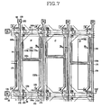
- Fig. 7 is a layout view of a TFT array panel for an LCD according to another embodiment of the invention.
- Fig. 8 is a sectional view of the TFT array panel shown in Fig. 7 taken along the line VIII-VIII'.
- Layered structures of the TFT panel 100 according to this embodiment are substantially the same as those shown in Figs. 1 , 3 and 4 .
- a plurality of gate lines 121 including gate electrodes 124 and end portions 129, a plurality of storage electrode lines 131 including storage electrodes 133a, 133b, and 133c may be formed on a substrate 110.
- a gate insulating layer 140, a plurality of semiconductor stripes 151 having projections 154, and a plurality of ohmic contacts 161 and 165 may be sequentially formed on the gate lines 121 and the storage electrodes lines 131
- a plurality of data lines 171 including source electrodes 173 and end portions 179, a plurality of drain electrodes 175 including coupling electrodes 176, and a plurality of metal pieces 172 may be formed on the ohmic contacts 161 and 165.
- a passivation layer 180 may be formed on the data lines 171, the drain electrodes 175, and exposed portions of the semiconductor stripes 151.
- a plurality of contact holes 181-185 may be provided at the passivation layer 180 and the gate insulating layer 140.
- a plurality of pixel electrodes 190 including sub-pixel electrodes 190a and 190b, a plurality of storage bridges 84, and a plurality of contact assistants 81 and 82 may be formed on the passivation layer 180.
- position of the transverse storage electrodes 133c is different according to red (R), green (G) and blue (B) pixels.
- the transverse storage electrode 133c of green pixel is disposed at the most upper portion of the pixel area
- the transverse storage electrode 133c of red pixel is disposed at the second most upper portion of the pixel area
- the transverse storage electrode 133c of blue pixel is disposed at the third most upper portion of the pixel area.
- the first sub-pixel electrode 190a and the second sub-pixel electrode 190b are divided into upper and lower on the transverse storage electrode 133c, respectively.
- the coupling electrode 176 extends along the storage electrodes 133a, 133b, and 133c and overlaps the storage electrodes 133a, 133b, and 133c.
- the coupling electrode 176 includes substantially longitudinal portions 176a and 176c respectively overlapping the storage electrodes 133a and 133b and a substantially transverse portion 133c overlapping the storage electrode 133c.
- Widths (W R , W G , W B ) of the coupling electrodes 176 are different according to the red (R), the green (G), and the blue (B) pixels. Accordingly, overlapping areas between the coupling electrodes 176 and the second sub-pixel electrodes 190b are different according to the red (R), the green (G), and the blue (B) pixels.
- coupling capacitances between the first sub-pixel electrodes 190a and the second sub-pixel electrodes 190b are different according to the red (R), the green (G), and the blue (B) pixels.
- voltage ratios of the second sub-pixel electrode 190b with respect to the first sub-pixel electrode 190a are different according to the red (R), the green (G), and the blue (B) pixels.
- Area ratios of the first sub-pixel electrodes 190a versus the second sub-pixel electrodes 190b are also different according to the red (R), the green (G), and the blue (B) pixels. These voltage ratio and area ratio may be adjusted to improve visibility and transmittance.
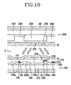
- Fig. 9 is a layout view of a TFT array panel for an LCD according to another embodiment of the invention.
- Fig. 10 is a sectional view of an LCD including the TFT array panel shown in Fig. 9 taken along the line X-X'.
- layered structures of the TFT panel 100 are substantially the same as those shown in Figs. 1 , 3 and 4 except for some features described below.
- a plurality of gate lines 121 including gate electrodes 124 and end portions 129, a plurality of storage electrode lines 131 including storage electrodes 133a, 133b, and 133c may be formed on a substrate 110, A gate insulating layer 140, a plurality of semiconductor stripes 151 having projections 154, and a plurality of ohmic contacts 161 and 165 may be sequentially formed on the gate lines 121 and the storage electrodes lines 131.
- a plurality of data lines 171 including source electrodes 173 and end portions 179, a plurality of drain electrodes 175 including coupling electrodes 176, and a plurality of metal pieces 172 may be formed on the ohmic contacts 161 and 165.
- a passivation layer 180 may be formed on the data lines 171, the drain electrodes 175, and exposed portions of the semiconductor stripes 151.
- a plurality of contact holes 181-185 may be provided at the passivation layer 180 and the gate insulating layer 140.
- a plurality of pixel electrodes 190 including sub-pixel electrodes 190a and 190b, a plurality of storage bridges 84 and a plurality of contact assistants 81 and 82 may be formed on the passivation layer 180.
- the semiconductor stripes 151 have substantially the same planar shapes as the data lines 171, the drain electrodes 175, and the underlying ohmic contacts 161 and 165. However, the semiconductor stripes 151 include some exposed portions, which are not covered with the data lines 171 and the drain electrodes 175, such as portions located between the source electrodes 173 and the drain electrodes 175.
- area ratios of the first sub-pixel electrodes 190a versus the second sub-pixel electrodes 190b are different according to the red (R), the green (G), and the blue (B) pixels.
- Area ratio of the second sub-pixel electrode 190b with respect to the first sub-pixel electrode 190a is preferably larger in red pixel than in green pixels or blue pixels. It is preferable that a ratio of an area of the second sub-pixel electrode 190b with respect to an area of the first sub-pixel electrode 190a decreases in an order of red, blue and green pixels.
- the TFT array panel for an LCD has coupling electrodes 176, amorphous silicon layers 154, and ohmic contact layers 165 that are formed under the coupling electrodes 176 with substantially the same shape.
- a photoresist layer having different thicknesses according to positions is used.
- Fig.11 is a layout view of a TFT array panel for an LCD according to another embodiment of the invention.
- Fig. 12 is a sectional view of an LCD including the TFT array panel shown in Fig. 1 taken along the line XII-XII'.
- layered structures of the TFT panel 100 according to this embodiment are substantially the same as those shown in Fig. 7 and Fig. 8 .
- the semiconductor stripes 151 have substantially the same planar shapes as the data lines 171, the drain electrodes 175, and the underlying ohmic contacts 161 and 165. However, the semiconductor stripes 151 include exposed portions, which are not covered with the data lines 171 and the drain electrodes 175, such as portions located between the source electrodes 173 and the drain electrodes 175.
- an LCD displays a lateral angle color tone that is substantially the same as a front color tone and has a high transmittance.
- cutouts in the pixel and common electrodes may be rearranged in various ways and shapes.
Claims (9)
- Eine Flüssigkristallanzeige, die folgendes umfasst:einen isolierenden Träger (10);eine Vielzahl von ersten Signalleitungen (121), die auf dem isolierenden Träger ausgebildet ist;eine Vielzahl von zweiten Signalleitungen (171), die die ersten Signalleitungen (121) kreuzt und von den ersten Signalleitungen isoliert ist;eine Vielzahl von Dünnschicht-Transistoren, die mit den ersten Signalleitungen und den zweiten Signalleitungen gekoppelt ist; undeine Vielzahl von Pixeln (190), die eine Vielzahl von ersten Sub-Pixel-Elektroden (190a) umfasst, die mit den DunnSchicht-Transistoren gekoppelt ist, und eine Vielzahl von zweiten Sub-Pixel-Elektroden (190b) umfasst, die mit den ersten Sub-Pixel-Elektroden (190a) kapazitiv gekoppelt ist,dadurch gekennzeichnet, dass die Pixel (190) einen Rot-Pixel, einen Grün-Pixel und einen Blau-Pixel umfassen, und
ein Spannungsverhältnis der zweiten Sub-Pixel-Elektrode (190b) hinsichtlich der ersten Sub-Pixel-Elektrode (190a) für jeden Rot-, Grün- und Blau-Pixel mindestens zwei verschiedene Werte aufweist. - Die Flüssigkristallanzeige nach Anspruch 1, wobei ein Verhältnis eines Bereichs der zweiten Sub-Pixel-Elektrode (190b) hinsichtlich eines Bereichs der ersten Sub-Pixel-Elektrode (190a) mindestens zwei verschiedene Werte aufweist.
- Die Flüssigkristallanzeige nach Anspruch 1, wobei das Spannungsverhältnis der zweiten Sub-Pixel-Elektrode (190b) hinsichtlich der ersten Sub-Pixel-Elektrode (190a) für den Grün-Pixel und den Blau-Pixel geringer ist als das Spannungsverhältnis der zweiten Sub-Pixel-Elektrode hinsichtlich der ersten Sub-Pixel-Elektrode für den Rot-Pixel.
- Die Flüssigkristallanzeige nach Anspruch 3, wobei das Spannungsverhältnis der zweiten Sub-Pixel-Elektrode (190b) hinsichtlich der ersten Sub-Pixel-Elektrode (190a) für den Grün-Pixel geringer ist als das Spannungsverhältnis der zweiten Sub-Pixel-Elektrode hinsichtlich der ersten Sub-Pixel-Elektrode für den Blau-Pixel.
- Die Flüssigkristallanzeige nach Anspruch 3, wobei das Spannungsverhältnis der zweiten Sub-Pixel-Elektrode (190b) hinsichtlich der ersten Sub-Pixel-Elektrode (190a) für den Rot-Pixel etwa 0,675 bis etwa 0,725 beträgt, wobei das Spannungsverhältnis der zweiten Sub-Pixel-Elektxode hinsichtlich der ersten Sub-Pixel-Elektrode für den Grün-Pixel etwa 0,600 bis etwa 0,650 beträgt, und wobei das Spannungsverhältnis der zweiten Sub-Pixel-Elektrode hinsichtlich der ersten Sub-Pixel-Elektrode für den Blau-Pixel etwa 0,650 bis etwa 0,700 beträgt.
- Ein Dünnschicht-Transistorarray-Panel, das folgendes umfasst:einen isolierenden Träger (10);eine Vielzahl von ersten Signalleitungen (121), die auf dem isolierenden Träger (10) ausgebildet ist;eine Vielzahl von zweiten Signalleitungen (171), die die ersten Signalleitungen (121) kreuzt und von den ersten Signalleitungen isoliert ist;eine Vielzahl von Dünnschicht-Transistoren, die mit den ersten Signalleitungen (121) und den zweiten Signalleitungen (171) gekoppelt ist; undeine Vielzahl von Pixeln (190), die eine Vielzahl von ersten sub-Pixel-Elektroden (190a) umfasst, die mit den Dünnschicht-Transistoren gekoppelt ist, eine Vielzahl von Kopplungselektroden (176) umfasst, die mit den Dünnschicht-Transistoren gekoppelt ist, und eine Vielzahl von zweiten Sub-Pixel-Elektroden (190b) umfasst, die die Kopplungselektroden (176) überlappt,dadurch gekennzeichnet, dass die Pixel (190) einen Rot-Pixel, einen Grün-Pixel und einen Blau-Pixel umfassen, und
ein Überlappungsbereich der Kopplungselektroden (176) und der zweiten Sub-Pixel-Elektroden (190b) für jeden Rot-, Grün- und Blau-Pixel mindestens zwei verschiedene Werte aufweist. - Das Dünnschicht-Transistorarray-Panel nach Anspruch 6, wobei der überlappungsbereich der Kopplungselektrode (176) und der zweiten Sub-Pixel-Elektrode (190b) für den Grün-Pixel und den Blau-Pixel geringer ist als der Überlappungsbereich der Kopplungselektrode und der zweiten Sub-Pixel-Elektrode für den Rot-Pixel.
- Das Dünnschicht-Transistorarray-Panel nach Anspruch 7, wobei der Überlappungsbereich der Kopplungselektrode (176) und der zweiten Sub-Pixel-Elektrode (190b) für den Grün-Pixel geringer ist als der Überlappungsbereich der Kopplungselektrode und der zweiten Sub-Pixel-Elektrode für den Blau-Pixel.
- Die Flüssigkristallanzeige nach Anspruch 1, wobei das Spannungsverhältnis der zweiten Sub-Pixel-Elektrode (190b) hinsichtlich der ersten Sub-Pixel-Elektrode (190a) zwischen dem Rot-Pixel, dem Grün-Pixel und dem Blau-Pixel unterschiedlich ist, so dass ein Helligkeitsverhältnis der Rotkomponente, der Grünkomponente und der Blaukomponente an einer seitlichen Position in einer Graustufe näher ist zu einem Helligkeitsverhältnis der Rotkomponente, der Grünkomponente und der Blaukomponente an einer vorderen Position in der Graustufe, und zwar verglichen zu dem Fall, in dem zwei unterschiedliche Spannungsverhältnisse zwischen dem Rot-Pixel, dem Grün-Pixel und dem Blau-Pixel nicht vorhanden sind.
Priority Applications (1)
| Application Number | Priority Date | Filing Date | Title |
|---|---|---|---|
| EP07114779A EP1860489A1 (de) | 2004-08-04 | 2005-08-02 | Dünnschichttransistoranordnungstafel und Flüssigkristallanzeige |
Applications Claiming Priority (2)
| Application Number | Priority Date | Filing Date | Title |
|---|---|---|---|
| KR1020040061397A KR20060012761A (ko) | 2004-08-04 | 2004-08-04 | 박막 트랜지스터 표시판 및 이를 포함하는 액정 표시 장치 |
| KR1020050013458A KR101188600B1 (ko) | 2005-02-18 | 2005-02-18 | 박막 트랜지스터 표시판 및 이를 포함하는 액정 표시 장치 |
Related Child Applications (1)
| Application Number | Title | Priority Date | Filing Date |
|---|---|---|---|
| EP07114779A Division EP1860489A1 (de) | 2004-08-04 | 2005-08-02 | Dünnschichttransistoranordnungstafel und Flüssigkristallanzeige |
Publications (2)
| Publication Number | Publication Date |
|---|---|
| EP1624332A1 EP1624332A1 (de) | 2006-02-08 |
| EP1624332B1 true EP1624332B1 (de) | 2008-05-14 |
Family
ID=35432308
Family Applications (2)
| Application Number | Title | Priority Date | Filing Date |
|---|---|---|---|
| EP05107132A Not-in-force EP1624332B1 (de) | 2004-08-04 | 2005-08-02 | Dünnfilmtransistorpanel und eine Flüssigkristallanzeige |
| EP07114779A Withdrawn EP1860489A1 (de) | 2004-08-04 | 2005-08-02 | Dünnschichttransistoranordnungstafel und Flüssigkristallanzeige |
Family Applications After (1)
| Application Number | Title | Priority Date | Filing Date |
|---|---|---|---|
| EP07114779A Withdrawn EP1860489A1 (de) | 2004-08-04 | 2005-08-02 | Dünnschichttransistoranordnungstafel und Flüssigkristallanzeige |
Country Status (6)
| Country | Link |
|---|---|
| US (1) | US7499129B2 (de) |
| EP (2) | EP1624332B1 (de) |
| JP (1) | JP2006048055A (de) |
| AT (1) | ATE395629T1 (de) |
| DE (1) | DE602005006677D1 (de) |
| TW (1) | TW200620675A (de) |
Families Citing this family (35)
| Publication number | Priority date | Publication date | Assignee | Title |
|---|---|---|---|---|
| KR20050098631A (ko) * | 2004-04-08 | 2005-10-12 | 삼성전자주식회사 | 액정 표시 장치 및 그에 사용되는 표시판 |
| US7221413B2 (en) * | 2004-08-05 | 2007-05-22 | Au Optronics Corporation | Thin film transistor array substrate and repairing method thereof |
| KR101189266B1 (ko) | 2004-09-24 | 2012-10-09 | 삼성디스플레이 주식회사 | 액정 표시 장치 |
| US7995177B2 (en) | 2005-06-09 | 2011-08-09 | Sharp Kabushiki Kaisha | Liquid crystal display device |
| KR101197049B1 (ko) * | 2005-06-27 | 2012-11-06 | 삼성디스플레이 주식회사 | 박막 트랜지스터 표시판 및 이를 포함하는 액정 표시 장치 |
| JP4570661B2 (ja) * | 2005-09-22 | 2010-10-27 | シャープ株式会社 | 液晶表示装置 |
| WO2007114471A1 (ja) | 2006-04-04 | 2007-10-11 | Sharp Kabushiki Kaisha | 液晶表示装置 |
| CN101427178B (zh) * | 2006-04-24 | 2010-12-01 | 夏普株式会社 | 液晶显示装置 |
| WO2008007583A1 (fr) * | 2006-07-14 | 2008-01-17 | Sharp Kabushiki Kaisha | Dispositif d'affichage à cristaux liquides |
| WO2008010332A1 (fr) * | 2006-07-20 | 2008-01-24 | Sharp Kabushiki Kaisha | dispositif d'affichage à cristaux liquides, et son procédé de fabrication |
| JP5148494B2 (ja) * | 2006-08-10 | 2013-02-20 | シャープ株式会社 | 液晶表示装置 |
| KR101254227B1 (ko) * | 2006-08-29 | 2013-04-19 | 삼성디스플레이 주식회사 | 표시패널 |
| EP2105785A4 (de) * | 2006-12-05 | 2010-06-23 | Sharp Kk | Flüssigkristallanzeigeeinrichtung |
| KR20080056481A (ko) * | 2006-12-18 | 2008-06-23 | 삼성전자주식회사 | 액정표시장치 및 이의 구동방법 |
| TWI351569B (en) * | 2007-06-07 | 2011-11-01 | Chunghwa Picture Tubes Ltd | Pixel structure |
| KR101443856B1 (ko) * | 2008-01-21 | 2014-09-25 | 삼성디스플레이 주식회사 | 액정 표시 장치 및 그에 포함되는 액정 조성물 |
| US9341896B2 (en) | 2008-01-21 | 2016-05-17 | Samsung Display Co., Ltd. | Liquid crystal display |
| JP5107421B2 (ja) * | 2008-03-31 | 2012-12-26 | シャープ株式会社 | アクティブマトリクス基板、液晶パネル、液晶表示装置、液晶表示ユニット、テレビジョン受像機 |
| TWI390309B (zh) | 2009-04-17 | 2013-03-21 | Chimei Innolux Corp | 液晶面板及應用其之液晶顯示裝置 |
| CN101930139B (zh) * | 2009-06-25 | 2015-01-07 | 群创光电股份有限公司 | 像素阵列基板、液晶显示装置及其驱动方法 |
| KR101666622B1 (ko) * | 2009-08-26 | 2016-10-17 | 삼성디스플레이 주식회사 | 광배향제 및 그것을 이용한 액정 표시 장치 |
| US20120194573A1 (en) * | 2009-09-25 | 2012-08-02 | Sharp Kabushiki Kaisha | Liquid crystal display device |
| RU2510066C1 (ru) | 2010-01-15 | 2014-03-20 | Шарп Кабусики Кайся | Жидкокристаллическое устройство отображения |
| US8358812B2 (en) | 2010-01-25 | 2013-01-22 | Apple Inc. | Image Preprocessing |
| TWI514058B (zh) * | 2011-11-11 | 2015-12-21 | Au Optronics Corp | 畫素陣列 |
| KR101917146B1 (ko) * | 2012-03-20 | 2018-11-12 | 삼성디스플레이 주식회사 | 표시 기판 |
| TWI526763B (zh) * | 2014-05-13 | 2016-03-21 | 友達光電股份有限公司 | 畫素結構、畫素陣列以及顯示面板 |
| TWI550329B (zh) * | 2014-07-07 | 2016-09-21 | 群創光電股份有限公司 | 顯示面板 |
| WO2016051575A1 (ja) * | 2014-10-02 | 2016-04-07 | 堺ディスプレイプロダクト株式会社 | 液晶表示装置 |
| CN104658502B (zh) * | 2015-03-09 | 2018-03-13 | 深圳市华星光电技术有限公司 | 一种液晶显示器的驱动方法及驱动装置 |
| CN104680995B (zh) * | 2015-03-09 | 2017-05-17 | 深圳市华星光电技术有限公司 | 一种液晶显示器的驱动方法及驱动装置 |
| CN104680993B (zh) * | 2015-03-09 | 2018-04-10 | 深圳市华星光电技术有限公司 | 一种液晶显示器的驱动方法及驱动装置 |
| CN104658504B (zh) * | 2015-03-09 | 2017-05-10 | 深圳市华星光电技术有限公司 | 一种液晶显示器的驱动方法及驱动装置 |
| JP7057134B2 (ja) * | 2018-01-10 | 2022-04-19 | キヤノン株式会社 | 表示装置及び撮像装置 |
| JP7073198B2 (ja) * | 2018-06-07 | 2022-05-23 | 株式会社ジャパンディスプレイ | 表示装置 |
Family Cites Families (15)
| Publication number | Priority date | Publication date | Assignee | Title |
|---|---|---|---|---|
| JPS6442633A (en) * | 1987-08-10 | 1989-02-14 | Koito Mfg Co Ltd | Liquid crystal display device for color display |
| US5126865A (en) * | 1990-12-31 | 1992-06-30 | Honeywell Inc. | Liquid crystal display with sub-pixels |
| JP3081357B2 (ja) * | 1992-04-15 | 2000-08-28 | 富士通株式会社 | 液晶表示装置及びその製造方法 |
| US5610739A (en) * | 1994-05-31 | 1997-03-11 | Matsushita Electric Industrial Co., Ltd. | Liquid crystal display unit with a plurality of subpixels |
| JP3311184B2 (ja) * | 1995-01-30 | 2002-08-05 | 松下電器産業株式会社 | 液晶表示装置 |
| JP3658849B2 (ja) * | 1996-03-29 | 2005-06-08 | セイコーエプソン株式会社 | 液晶表示素子及びその製造方法 |
| JPH10115820A (ja) * | 1996-10-09 | 1998-05-06 | Canon Inc | 表示素子の駆動法及び表示装置 |
| KR100465107B1 (ko) | 1997-05-22 | 2005-04-06 | 삼성전자주식회사 | 과전압보호회로 |
| US6100861A (en) * | 1998-02-17 | 2000-08-08 | Rainbow Displays, Inc. | Tiled flat panel display with improved color gamut |
| KR100508059B1 (ko) | 1998-04-17 | 2005-11-21 | 삼성전자주식회사 | 수직 배향 모드 액정 표시 장치 |
| KR19990084238A (ko) | 1998-05-02 | 1999-12-06 | 오평희 | 광시야 액정표시소자 및 액정표시소자 구동방법 |
| TWI275859B (en) | 2002-02-20 | 2007-03-11 | Sharp Kk | Liquid crystal display device's substrate, liquid crystal display device including the same, and manufacturing method of the same |
| JP4342200B2 (ja) | 2002-06-06 | 2009-10-14 | シャープ株式会社 | 液晶表示装置 |
| JP4373071B2 (ja) | 2002-09-10 | 2009-11-25 | 大林精工株式会社 | 高速応答液晶表示装置とその駆動方法 |
| KR100980016B1 (ko) * | 2003-08-04 | 2010-09-03 | 삼성전자주식회사 | 박막 트랜지스터 표시판 |
-
2005
- 2005-07-29 TW TW094125813A patent/TW200620675A/zh unknown
- 2005-08-02 EP EP05107132A patent/EP1624332B1/de not_active Not-in-force
- 2005-08-02 DE DE602005006677T patent/DE602005006677D1/de active Active
- 2005-08-02 AT AT05107132T patent/ATE395629T1/de not_active IP Right Cessation
- 2005-08-02 EP EP07114779A patent/EP1860489A1/de not_active Withdrawn
- 2005-08-03 US US11/195,779 patent/US7499129B2/en active Active - Reinstated
- 2005-08-04 JP JP2005226423A patent/JP2006048055A/ja not_active Withdrawn
Also Published As
| Publication number | Publication date |
|---|---|
| TW200620675A (en) | 2006-06-16 |
| EP1624332A1 (de) | 2006-02-08 |
| JP2006048055A (ja) | 2006-02-16 |
| ATE395629T1 (de) | 2008-05-15 |
| EP1860489A1 (de) | 2007-11-28 |
| US7499129B2 (en) | 2009-03-03 |
| US20060028589A1 (en) | 2006-02-09 |
| DE602005006677D1 (de) | 2008-06-26 |
Similar Documents
| Publication | Publication Date | Title |
|---|---|---|
| EP1624332B1 (de) | Dünnfilmtransistorpanel und eine Flüssigkristallanzeige | |
| US7339634B2 (en) | Thin film transistor array panel with varying coupling capacitance between the first and second pixel electrode | |
| US7379143B2 (en) | Liquid crystal display having predetermined steepness of light transmittance within a predetermined range on light transmittance gradient for improved visibility | |
| US7440040B2 (en) | Liquid crystal display device with storage electrode extension | |
| US7663617B2 (en) | Thin film transistor array panel and liquid crystal display including the panel | |
| US7619694B2 (en) | Thin film transistor array panel and manufacturing method thereof | |
| US8194199B2 (en) | Liquid crystal display device having a ratio of liquid crystal capacitances equal to a ratio of parasitic capacitances | |
| US8129723B2 (en) | Liquid crystal display and panel therefor | |
| US7777823B2 (en) | Thin film transistor array panel | |
| US7486343B2 (en) | TFT array panel having a two-portion coupling electrode extending from drain electrode in different directions with first portion extending along a gap between two overlapping subpixel electrodes thereon and second portion extending in same direction as data line | |
| US7944535B2 (en) | Liquid crystal display and a method for manufacturing the same | |
| US7973899B2 (en) | Thin film transistor array panel with capacitive coupling between adjacent pixel areas | |
| US7733434B2 (en) | Liquid crystal display including buffer electrodes with higher voltage than pixel electrodes, on same layer with pixel electrodes, and overlapping a gate line | |
| US7773165B2 (en) | Liquid crystal display | |
| US7474363B2 (en) | Liquid crystal display and panel therefor | |
| US20070002248A1 (en) | Liquid crystal display and panel therefor | |
| US20060092116A1 (en) | Liquid crystal display | |
| KR101188600B1 (ko) | 박막 트랜지스터 표시판 및 이를 포함하는 액정 표시 장치 | |
| KR20050076402A (ko) | 액정 표시 장치 및 이를 위한 박막 트랜지스터 표시판 |
Legal Events
| Date | Code | Title | Description |
|---|---|---|---|
| PUAI | Public reference made under article 153(3) epc to a published international application that has entered the european phase |
Free format text: ORIGINAL CODE: 0009012 |
|
| AK | Designated contracting states |
Kind code of ref document: A1 Designated state(s): AT BE BG CH CY CZ DE DK EE ES FI FR GB GR HU IE IS IT LI LT LU LV MC NL PL PT RO SE SI SK TR |
|
| AX | Request for extension of the european patent |
Extension state: AL BA HR MK YU |
|
| RIN1 | Information on inventor provided before grant (corrected) |
Inventor name: SON, JONG-HO102-504, HANSOL APT. Inventor name: CHUNG, DONG-HOON318-2205 DUGYEONMAEUL Inventor name: LYU, JAE-JIN Inventor name: LEE, JUN-WOO506-1307 HANGARAM SEGYEONG APT. Inventor name: SHIN, YONG-HWAN336-606 CHEONGMYEONGMAEUL Inventor name: UM, YOON-SUNG216-1702 SSANGYONG APT. Inventor name: CHANG, HAK-SUN Inventor name: KIM, HYUN-WUK Inventor name: LEE, CHANG-HUN104-1205 YEHYEONMAEUL |
|
| RIN1 | Information on inventor provided before grant (corrected) |
Inventor name: LYU, JAE-JIN Inventor name: UM, YOON-SUNG216-1702 SSANGYONG APT. Inventor name: SHIN, YONG-HWAN336-606 CHEONGMYEONGMAEUL Inventor name: SON, JONG-HO102-504, HANSOL APT. Inventor name: CHUNG, DONG-HOON318-2205 DUGYEONMAEUL Inventor name: KIM, HYUN-WUK Inventor name: CHANG, HAK-SUN Inventor name: LEE, JUN-WOO112-204 INDEOKWON SAMSUNG APT. Inventor name: LEE, CHANG-HUN104-1205 HYUNDAI HOMETOWN |
|
| 17P | Request for examination filed |
Effective date: 20060302 |
|
| AKX | Designation fees paid |
Designated state(s): AT BE BG CH CY CZ DE DK EE ES FI FR GB GR HU IE IS IT LI LT LU LV MC NL PL PT RO SE SI SK TR |
|
| GRAP | Despatch of communication of intention to grant a patent |
Free format text: ORIGINAL CODE: EPIDOSNIGR1 |
|
| GRAS | Grant fee paid |
Free format text: ORIGINAL CODE: EPIDOSNIGR3 |
|
| GRAA | (expected) grant |
Free format text: ORIGINAL CODE: 0009210 |
|
| AK | Designated contracting states |
Kind code of ref document: B1 Designated state(s): AT BE BG CH CY CZ DE DK EE ES FI FR GB GR HU IE IS IT LI LT LU LV MC NL PL PT RO SE SI SK TR |
|
| REG | Reference to a national code |
Ref country code: GB Ref legal event code: FG4D |
|
| REG | Reference to a national code |
Ref country code: CH Ref legal event code: EP |
|
| REG | Reference to a national code |
Ref country code: IE Ref legal event code: FG4D Free format text: LANGUAGE OF EP DOCUMENT: FRENCH |
|
| REF | Corresponds to: |
Ref document number: 602005006677 Country of ref document: DE Date of ref document: 20080626 Kind code of ref document: P |
|
| PG25 | Lapsed in a contracting state [announced via postgrant information from national office to epo] |
Ref country code: SI Free format text: LAPSE BECAUSE OF FAILURE TO SUBMIT A TRANSLATION OF THE DESCRIPTION OR TO PAY THE FEE WITHIN THE PRESCRIBED TIME-LIMIT Effective date: 20080514 |
|
| PG25 | Lapsed in a contracting state [announced via postgrant information from national office to epo] |
Ref country code: ES Free format text: LAPSE BECAUSE OF FAILURE TO SUBMIT A TRANSLATION OF THE DESCRIPTION OR TO PAY THE FEE WITHIN THE PRESCRIBED TIME-LIMIT Effective date: 20080825 Ref country code: FI Free format text: LAPSE BECAUSE OF FAILURE TO SUBMIT A TRANSLATION OF THE DESCRIPTION OR TO PAY THE FEE WITHIN THE PRESCRIBED TIME-LIMIT Effective date: 20080514 |
|
| NLV1 | Nl: lapsed or annulled due to failure to fulfill the requirements of art. 29p and 29m of the patents act | ||
| PG25 | Lapsed in a contracting state [announced via postgrant information from national office to epo] |
Ref country code: NL Free format text: LAPSE BECAUSE OF FAILURE TO SUBMIT A TRANSLATION OF THE DESCRIPTION OR TO PAY THE FEE WITHIN THE PRESCRIBED TIME-LIMIT Effective date: 20080514 Ref country code: PL Free format text: LAPSE BECAUSE OF FAILURE TO SUBMIT A TRANSLATION OF THE DESCRIPTION OR TO PAY THE FEE WITHIN THE PRESCRIBED TIME-LIMIT Effective date: 20080514 Ref country code: AT Free format text: LAPSE BECAUSE OF FAILURE TO SUBMIT A TRANSLATION OF THE DESCRIPTION OR TO PAY THE FEE WITHIN THE PRESCRIBED TIME-LIMIT Effective date: 20080514 Ref country code: LV Free format text: LAPSE BECAUSE OF FAILURE TO SUBMIT A TRANSLATION OF THE DESCRIPTION OR TO PAY THE FEE WITHIN THE PRESCRIBED TIME-LIMIT Effective date: 20080514 |
|
| PG25 | Lapsed in a contracting state [announced via postgrant information from national office to epo] |
Ref country code: IS Free format text: LAPSE BECAUSE OF FAILURE TO SUBMIT A TRANSLATION OF THE DESCRIPTION OR TO PAY THE FEE WITHIN THE PRESCRIBED TIME-LIMIT Effective date: 20080914 |
|
| PG25 | Lapsed in a contracting state [announced via postgrant information from national office to epo] |
Ref country code: DK Free format text: LAPSE BECAUSE OF FAILURE TO SUBMIT A TRANSLATION OF THE DESCRIPTION OR TO PAY THE FEE WITHIN THE PRESCRIBED TIME-LIMIT Effective date: 20080514 Ref country code: LT Free format text: LAPSE BECAUSE OF FAILURE TO SUBMIT A TRANSLATION OF THE DESCRIPTION OR TO PAY THE FEE WITHIN THE PRESCRIBED TIME-LIMIT Effective date: 20080514 Ref country code: SE Free format text: LAPSE BECAUSE OF FAILURE TO SUBMIT A TRANSLATION OF THE DESCRIPTION OR TO PAY THE FEE WITHIN THE PRESCRIBED TIME-LIMIT Effective date: 20080814 Ref country code: CZ Free format text: LAPSE BECAUSE OF FAILURE TO SUBMIT A TRANSLATION OF THE DESCRIPTION OR TO PAY THE FEE WITHIN THE PRESCRIBED TIME-LIMIT Effective date: 20080514 |
|
| PG25 | Lapsed in a contracting state [announced via postgrant information from national office to epo] |
Ref country code: RO Free format text: LAPSE BECAUSE OF FAILURE TO SUBMIT A TRANSLATION OF THE DESCRIPTION OR TO PAY THE FEE WITHIN THE PRESCRIBED TIME-LIMIT Effective date: 20080514 Ref country code: BE Free format text: LAPSE BECAUSE OF FAILURE TO SUBMIT A TRANSLATION OF THE DESCRIPTION OR TO PAY THE FEE WITHIN THE PRESCRIBED TIME-LIMIT Effective date: 20080514 Ref country code: PT Free format text: LAPSE BECAUSE OF FAILURE TO SUBMIT A TRANSLATION OF THE DESCRIPTION OR TO PAY THE FEE WITHIN THE PRESCRIBED TIME-LIMIT Effective date: 20081014 Ref country code: SK Free format text: LAPSE BECAUSE OF FAILURE TO SUBMIT A TRANSLATION OF THE DESCRIPTION OR TO PAY THE FEE WITHIN THE PRESCRIBED TIME-LIMIT Effective date: 20080514 |
|
| PLBE | No opposition filed within time limit |
Free format text: ORIGINAL CODE: 0009261 |
|
| STAA | Information on the status of an ep patent application or granted ep patent |
Free format text: STATUS: NO OPPOSITION FILED WITHIN TIME LIMIT |
|
| PG25 | Lapsed in a contracting state [announced via postgrant information from national office to epo] |
Ref country code: MC Free format text: LAPSE BECAUSE OF NON-PAYMENT OF DUE FEES Effective date: 20080831 |
|
| 26N | No opposition filed |
Effective date: 20090217 |
|
| PG25 | Lapsed in a contracting state [announced via postgrant information from national office to epo] |
Ref country code: BG Free format text: LAPSE BECAUSE OF FAILURE TO SUBMIT A TRANSLATION OF THE DESCRIPTION OR TO PAY THE FEE WITHIN THE PRESCRIBED TIME-LIMIT Effective date: 20080814 Ref country code: EE Free format text: LAPSE BECAUSE OF FAILURE TO SUBMIT A TRANSLATION OF THE DESCRIPTION OR TO PAY THE FEE WITHIN THE PRESCRIBED TIME-LIMIT Effective date: 20080514 |
|
| REG | Reference to a national code |
Ref country code: IE Ref legal event code: MM4A |
|
| PG25 | Lapsed in a contracting state [announced via postgrant information from national office to epo] |
Ref country code: IE Free format text: LAPSE BECAUSE OF NON-PAYMENT OF DUE FEES Effective date: 20080802 |
|
| PG25 | Lapsed in a contracting state [announced via postgrant information from national office to epo] |
Ref country code: IT Free format text: LAPSE BECAUSE OF FAILURE TO SUBMIT A TRANSLATION OF THE DESCRIPTION OR TO PAY THE FEE WITHIN THE PRESCRIBED TIME-LIMIT Effective date: 20080514 |
|
| REG | Reference to a national code |
Ref country code: CH Ref legal event code: PL |
|
| PG25 | Lapsed in a contracting state [announced via postgrant information from national office to epo] |
Ref country code: CH Free format text: LAPSE BECAUSE OF NON-PAYMENT OF DUE FEES Effective date: 20090831 Ref country code: LI Free format text: LAPSE BECAUSE OF NON-PAYMENT OF DUE FEES Effective date: 20090831 |
|
| PG25 | Lapsed in a contracting state [announced via postgrant information from national office to epo] |
Ref country code: CY Free format text: LAPSE BECAUSE OF FAILURE TO SUBMIT A TRANSLATION OF THE DESCRIPTION OR TO PAY THE FEE WITHIN THE PRESCRIBED TIME-LIMIT Effective date: 20080514 Ref country code: HU Free format text: LAPSE BECAUSE OF FAILURE TO SUBMIT A TRANSLATION OF THE DESCRIPTION OR TO PAY THE FEE WITHIN THE PRESCRIBED TIME-LIMIT Effective date: 20081115 Ref country code: LU Free format text: LAPSE BECAUSE OF NON-PAYMENT OF DUE FEES Effective date: 20080802 |
|
| PG25 | Lapsed in a contracting state [announced via postgrant information from national office to epo] |
Ref country code: TR Free format text: LAPSE BECAUSE OF FAILURE TO SUBMIT A TRANSLATION OF THE DESCRIPTION OR TO PAY THE FEE WITHIN THE PRESCRIBED TIME-LIMIT Effective date: 20080514 |
|
| PG25 | Lapsed in a contracting state [announced via postgrant information from national office to epo] |
Ref country code: GR Free format text: LAPSE BECAUSE OF FAILURE TO SUBMIT A TRANSLATION OF THE DESCRIPTION OR TO PAY THE FEE WITHIN THE PRESCRIBED TIME-LIMIT Effective date: 20080815 |
|
| REG | Reference to a national code |
Ref country code: FR Ref legal event code: TP Owner name: SAMSUNG DISPLAY CO. LTD, KR Effective date: 20130226 |
|
| REG | Reference to a national code |
Ref country code: GB Ref legal event code: 732E Free format text: REGISTERED BETWEEN 20130307 AND 20130313 |
|
| REG | Reference to a national code |
Ref country code: DE Ref legal event code: R082 Ref document number: 602005006677 Country of ref document: DE Representative=s name: DR. WEITZEL & PARTNER, DE |
|
| REG | Reference to a national code |
Ref country code: DE Ref legal event code: R082 Ref document number: 602005006677 Country of ref document: DE Representative=s name: FARAGO PATENTANWAELTE, DE Effective date: 20130422 Ref country code: DE Ref legal event code: R082 Ref document number: 602005006677 Country of ref document: DE Representative=s name: DR. WEITZEL & PARTNER, DE Effective date: 20130422 Ref country code: DE Ref legal event code: R081 Ref document number: 602005006677 Country of ref document: DE Owner name: SAMSUNG DISPLAY CO., LTD., KR Free format text: FORMER OWNER: SAMSUNG ELECTRONICS CO., LTD., SUWON-SI, KR Effective date: 20130422 Ref country code: DE Ref legal event code: R082 Ref document number: 602005006677 Country of ref document: DE Representative=s name: SCHIEBER - FARAGO, DE Effective date: 20130422 Ref country code: DE Ref legal event code: R081 Ref document number: 602005006677 Country of ref document: DE Owner name: SAMSUNG DISPLAY CO., LTD., YONGIN-CITY, KR Free format text: FORMER OWNER: SAMSUNG ELECTRONICS CO., LTD., SUWON-SI, GYEONGGI-DO, KR Effective date: 20130422 |
|
| REG | Reference to a national code |
Ref country code: DE Ref legal event code: R082 Ref document number: 602005006677 Country of ref document: DE Representative=s name: SCHIEBER - FARAGO, DE Ref country code: DE Ref legal event code: R082 Ref document number: 602005006677 Country of ref document: DE Representative=s name: FARAGO PATENTANWAELTE, DE |
|
| REG | Reference to a national code |
Ref country code: FR Ref legal event code: PLFP Year of fee payment: 11 |
|
| PGFP | Annual fee paid to national office [announced via postgrant information from national office to epo] |
Ref country code: GB Payment date: 20150811 Year of fee payment: 11 Ref country code: DE Payment date: 20150811 Year of fee payment: 11 |
|
| PGFP | Annual fee paid to national office [announced via postgrant information from national office to epo] |
Ref country code: FR Payment date: 20150625 Year of fee payment: 11 |
|
| REG | Reference to a national code |
Ref country code: DE Ref legal event code: R119 Ref document number: 602005006677 Country of ref document: DE |
|
| GBPC | Gb: european patent ceased through non-payment of renewal fee |
Effective date: 20160802 |
|
| REG | Reference to a national code |
Ref country code: FR Ref legal event code: ST Effective date: 20170428 |
|
| PG25 | Lapsed in a contracting state [announced via postgrant information from national office to epo] |
Ref country code: FR Free format text: LAPSE BECAUSE OF NON-PAYMENT OF DUE FEES Effective date: 20160831 Ref country code: DE Free format text: LAPSE BECAUSE OF NON-PAYMENT OF DUE FEES Effective date: 20170301 Ref country code: GB Free format text: LAPSE BECAUSE OF NON-PAYMENT OF DUE FEES Effective date: 20160802 |