EP1608057A1 - Schutzschaltung zur Reduzierung elektrischer Störungen beim Betrieb eines Gleichstrommotors - Google Patents
Schutzschaltung zur Reduzierung elektrischer Störungen beim Betrieb eines Gleichstrommotors Download PDFInfo
- Publication number
- EP1608057A1 EP1608057A1 EP05010703A EP05010703A EP1608057A1 EP 1608057 A1 EP1608057 A1 EP 1608057A1 EP 05010703 A EP05010703 A EP 05010703A EP 05010703 A EP05010703 A EP 05010703A EP 1608057 A1 EP1608057 A1 EP 1608057A1
- Authority
- EP
- European Patent Office
- Prior art keywords
- voltage
- protection circuit
- transistor
- diode
- circuit according
- Prior art date
- Legal status (The legal status is an assumption and is not a legal conclusion. Google has not performed a legal analysis and makes no representation as to the accuracy of the status listed.)
- Granted
Links
- 230000001052 transient effect Effects 0.000 claims description 13
- 238000004804 winding Methods 0.000 claims description 6
- 230000002441 reversible effect Effects 0.000 claims description 4
- 230000005669 field effect Effects 0.000 claims 4
- 239000003990 capacitor Substances 0.000 description 22
- 238000010586 diagram Methods 0.000 description 8
- 230000000670 limiting effect Effects 0.000 description 6
- 230000002829 reductive effect Effects 0.000 description 4
- XEEYBQQBJWHFJM-UHFFFAOYSA-N Iron Chemical compound [Fe] XEEYBQQBJWHFJM-UHFFFAOYSA-N 0.000 description 2
- 238000001914 filtration Methods 0.000 description 2
- 238000012986 modification Methods 0.000 description 2
- 230000004048 modification Effects 0.000 description 2
- 230000001681 protective effect Effects 0.000 description 2
- 230000004913 activation Effects 0.000 description 1
- 230000002238 attenuated effect Effects 0.000 description 1
- 230000015572 biosynthetic process Effects 0.000 description 1
- 230000001276 controlling effect Effects 0.000 description 1
- 238000011161 development Methods 0.000 description 1
- 230000018109 developmental process Effects 0.000 description 1
- 229910052742 iron Inorganic materials 0.000 description 1
- 230000001105 regulatory effect Effects 0.000 description 1
- 238000004513 sizing Methods 0.000 description 1
Images


Classifications
-
- H—ELECTRICITY
- H02—GENERATION; CONVERSION OR DISTRIBUTION OF ELECTRIC POWER
- H02P—CONTROL OR REGULATION OF ELECTRIC MOTORS, ELECTRIC GENERATORS OR DYNAMO-ELECTRIC CONVERTERS; CONTROLLING TRANSFORMERS, REACTORS OR CHOKE COILS
- H02P7/00—Arrangements for regulating or controlling the speed or torque of electric DC motors
- H02P7/06—Arrangements for regulating or controlling the speed or torque of electric DC motors for regulating or controlling an individual DC dynamo-electric motor by varying field or armature current
- H02P7/18—Arrangements for regulating or controlling the speed or torque of electric DC motors for regulating or controlling an individual DC dynamo-electric motor by varying field or armature current by master control with auxiliary power
- H02P7/24—Arrangements for regulating or controlling the speed or torque of electric DC motors for regulating or controlling an individual DC dynamo-electric motor by varying field or armature current by master control with auxiliary power using discharge tubes or semiconductor devices
- H02P7/28—Arrangements for regulating or controlling the speed or torque of electric DC motors for regulating or controlling an individual DC dynamo-electric motor by varying field or armature current by master control with auxiliary power using discharge tubes or semiconductor devices using semiconductor devices
-
- H—ELECTRICITY
- H03—ELECTRONIC CIRCUITRY
- H03K—PULSE TECHNIQUE
- H03K17/00—Electronic switching or gating, i.e. not by contact-making and –breaking
- H03K17/16—Modifications for eliminating interference voltages or currents
- H03K17/161—Modifications for eliminating interference voltages or currents in field-effect transistor switches
- H03K17/165—Modifications for eliminating interference voltages or currents in field-effect transistor switches by feedback from the output circuit to the control circuit
Definitions
- the invention relates to a protection circuit for reducing electrical noise when operating a DC motor and a DC motor with a corresponding protection circuit.
- Such electrical noise includes both high-energy transient impulses, as well as low-voltage disturbances in the Frequency range from 50 Hz to 20 KHz with amplitudes of 6 V peak-to-peak.
- Protection circuits used in the prior art include varistors and LC filters or filter capacitors to DC motors from electrical noise too protect.
- the varistors serve to absorb the high-energy transient pulses, and the LC filters or filter capacitors are used to filter out the Low-voltage interference. Due to the required size, the limited Working temperature and the limited life of LC filters or Sieve capacitors, however, their use is complicated and limited possible. The use of varistors is due to the required sizing the varistors consuming and expensive.
- the object of the present invention is to provide an improved protection circuit for Reduction of electrical interference during operation of DC motors provide. This object is achieved by a protection circuit according to claim 1 or achieved by a DC motor according to claim 14.
- the invention is based on the finding that a reduction of electrical Disturbances in the operation of DC motors through an active protection circuit can be achieved.
- An active protection circuit is preferably provided by a Analyzer circuit, a power controller and a control for the Power controller realized.
- a basic idea of the invention consists in the fact that the Control drives the power controller such that the power controller with a affected by electrical interference input voltage of the protection circuit, to an associated DC motor, a substantially electrical Disruptions supply free supply voltage.
- This is the analyzer circuit provided that analyzes the input voltage and the electrical noise in detected this input voltage.
- the power controller is called Longitudinal transistor formed.
- the activation causes the series transistor Fully conductive is when the input voltage is substantially free of electrical Disruptions is.
- the input voltage to the DC motor in Essentially supplied without losses as a supply voltage.
- electrical disturbances in the form of transient pulses causes the drive that the series transistor the amplitude of the generated by the protection circuit Supply voltage limited to a predetermined value.
- the analyzer circuit comprises an RC element.
- the RC member are in case of electrical disturbances in the form of Low voltages with frequencies from 50 Hz to 20 kHz in the input voltage the Frequency components filtered out.
- the invention is here not limited to a specific engine type.
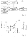
- the protection circuit 100 according to the invention is designed to reduce electrical interference in an output signal of a supply source 10 during operation of a load 70.
- the protection circuit 100 supplies the output signal of the supply source 10 via a polarity reversal protection 20 to an analyzer circuit 30 and to a power regulator 60.
- a driver 40 receives the output of the analyzer circuit 30 and the output of an auxiliary voltage source 50. On the output side, the driver 40 is connected to the power regulator 60.
- the output of the power controller 60 is supplied to the load 70 and is substantially free of electrical noise.
- the Supply source 10 a required for the operation of the load 70 Supply voltage ready.
- the supply voltage supplied to the reverse polarity protection 20 To an incorrect voltage polarity or negative
- the supply voltage supplied to the reverse polarity protection 20 To avoid voltage disturbances on the load 70, the supply voltage supplied to the reverse polarity protection 20.
- the polarity reversal protection 20 clears signal components that Negative voltage disturbances cause and block signal forwarding with an incorrect polarity of the supply voltage.
- the analyzer circuit 30 analyzes the supply voltage and controls the Control 40.
- the driver 40 controls the power controller 60 using from a substantially constant auxiliary voltage from the auxiliary voltage source 50 at. More specifically, the driver 40 is driven by the analyzer circuit 30 regulated such that the power regulator 60 a trouble-free supply voltage Essentially without losses of the load 70 supplies. Upon the occurrence of electrical Disturbances in the supply voltage, the control 40 is accordingly adapted to the influence of these electrical noise on the load 70 below Use of the power controller 60 to reduce.
- the Power regulator 60 that the load 70 supplied substantially trouble-free energy and for the load 70, harmful voltage pulses, e.g. energy Transient pulses are sufficiently attenuated.
- the exemplary protection circuit 200 includes a supply voltage source 12 and a load 72 shown as a resistor.
- a plus line of the supply voltage source 12 is connected to the anode side of a diode 22.
- the output signal of the diode 22 is supplied from the cathode side of the diode 22 via a resistor 32 to the negative pole of an auxiliary voltage source 52.
- the output signal of the diode 22 is further supplied to the cathode side of a diode 36 and the drain region of a series transistor (MOSFET) 62.
- MOSFET series transistor
- the anode side of the diode 36 and the negative pole of the auxiliary voltage source 52 are connected via a storage capacitor 34 to ground.
- the plus pole of the auxiliary voltage source is connected to the gate of the series transistor 62.
- the plus pole of the auxiliary voltage source 52 is connected to ground via a storage capacitor 66 and a Zener diode 64 arranged parallel to the storage capacitor 66.
- the source region of the series transistor is connected on the one hand via the load 72 and on the other hand via an intermediate circuit capacitor 74 to ground.
- the diode forms 22 a polarity reversal protection (eg., Verpolschutz 20 of Fig. 1), which the load 72 against protects wrong connection.
- the series transistor 62, the storage capacitor 66 and the Zener diode 64 form a power regulator (eg, power regulator 60 of FIG. 1).
- the resistor 32, the capacitor 34 and the diode 36 form a Analyzer circuit (eg analyzer circuit 30 of Fig. 1).
- One on the diode 36 falling diode voltage and one of the auxiliary voltage source 52 eg. Auxiliary voltage source 50 of FIG. 1), substantially constant Auxiliary voltage, constitute a drive (e.g., driver 40 of FIG Longitudinal transistor 62 (or power regulator 60).
- the operation of the protection circuit 200 is explained in more detail below.
- the supply voltage source 12 provides the protection circuit 200 a Input voltage 302 ready.
- the input voltage 302 is preferably one in the Essentially constant DC voltage with an amplitude of +13.2 V, generated by a power supply or a battery is generated.
- the diode 22 is only conductive for one Input voltage with a correct polarity, with negative voltage disturbances be blocked in the input voltage.
- An exemplary input voltage 302 is illustrated in Fig. 3. Based on the input voltage 302 of FIG. 3 generates the Diode 22 is a voltage 304, which is also illustrated in FIG.
- the voltage 304 causes a voltage drop across the diode 36, which causes the formation of a corresponding diode voltage causes.
- the sum of the diode voltage and the The auxiliary voltage generated by the auxiliary voltage source 52 forms a control voltage for the series transistor 62.
- the auxiliary voltage is preferably a substantially one constant DC voltage with an amplitude of +2 V.
- the control voltage is Preferably configured such that it approximately the switching threshold of Longitudinal transistor 62 corresponds.
- the control voltage is adapted to the Longitudinal transistor 62 in the ohmic region fully conductive to control, if one of the Supply voltage source 302 supplied substantially free of electrical interference is.
- the protection circuit 200 With the occurrence of electrical disturbances in the form of transient pulses with Voltage pulses of up to +100 V in the input voltage 302 and thus in the Voltage 304 turns off the diode 36.
- This causes the protection circuit 200 how a power supply works - with an output voltage that of the Storage capacitor 66 is provided and from the Zener diode 64 to the Zener diode voltage is limited.
- the amount of tension 304 on the occurrence of high-energy transient pulses through the Zener diode 64 limits a given value.
- the zener diode 64 is such dimensioned that this predetermined value about 25% above the value of trouble-free voltage 304 is located. This ensures that the zener diode 64 is addressed only when high-energy transient pulses occur. In the case of a fault-free input voltage 302, the Zener diode 64 has no influence on the function of the protection circuit 200.
- the supply voltage 306 At the output of the protection circuit 200 and thus to the load 72 is accordingly a supply voltage 306.
- the supply voltage 306 are opposite voltage 304 electrical disturbances in the form of high-energy Transient pulses and low voltages with frequencies from 50 Hz to 20 KHz reduced.
- An exemplary supply voltage 306 is also illustrated in FIG.
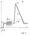
- FIG. 3 shows a schematic illustration 300 of exemplary time profiles of the voltages 302, 304 and 306 of FIG. 2.
- the input voltage 302 represents a nominal voltage for operating the load 72.
- the input voltage 302 has an area 310, which exemplifies a represents negative voltage component, d. H. an input voltage with wrong Polarity.
- the input voltage 302 has a region 320, which Illustrated example low-voltage interference.
- the voltage 304 corresponds to the input voltage 302, of which the negative Voltage component in the region 310 through the diode 22 formed by the Reverse polarity protection removed and the diode voltage of the diode 22 was deducted.
- the supply voltage 306 corresponds to the voltage 304 at which the Low-voltage disturbances in the range 320 and the transient pulse in the range 330 were reduced.
- the supply voltage 306 in the area 320 after filtering out the frequency components of Low voltage disturbances and lowering the control voltage of the series transistor 62, as described above, reduced.
- the transient pulse is in Area 330 has not been completely removed from the voltage 304, but in the Supply voltage 306 only substantially to the voltage of the zener diode 64 has been reduced, i. to a DC voltage with an amplitude of approximately +15 V.
- FIG. 4 is a highly simplified circuit diagram of an exemplary electrical noise reduction protection circuit 400 according to a second embodiment of the present invention.
- a diode circuit in which, by way of example, four diodes 54, 55, 56, and 57 are connected in series is arranged between the gate of the series transistor 62 and the capacitor 34. Parallel to the four series-connected diodes 54, 55, 56 and 57, a resistor between the gate of the series transistor 62 and the resistor 32 is arranged.
- the protection circuit 400 has a voltage source 82, which is connected via a current limiting resistor 84 to the anode side of a diode 86.
- the cathode side of the diode 86 is connected on the one hand via a capacitor 87 to ground and on the other hand via a resistor 88 to the cathode side of the Zener diode 64.
- the rest of the circuit arrangement corresponds to that of FIG. 2.
- the protection circuit 400 replaces the parallel connection of the four diodes 54, 55, 56 and 57 with the resistor 53, the auxiliary voltage source 52 of the protective circuit 200 of Fig. 2.
- the four diodes 54, 55, 56 and 57 are formed such that at them a voltage drop occurs, which is the auxiliary voltage of the auxiliary voltage source 52 essentially corresponds.
- a voltage drop of +2 V a voltage of approximately +0.5 V at each of the four diodes arise.
- the series connection of the four diodes 54, 55, 56 and 57 can as well as a correspondingly dimensioned zener diode or light emitting diode or a Combination of different types of diodes can be used.
- the voltage drop across the diodes 54, 55, 56 and 57 is made possible by the Provision of an auxiliary input voltage U_AUX_IN at the voltage source 82 with an amplitude of about +18 V.
- the resistor 84 is a Current limiting to protect downstream elements.
- the diode 86 causes by the auxiliary voltage U_AUX_IN only an increase of the voltage U_710 am Capacitor 66 can take place (principle of the charge pump).
- the Auxiliary input voltage U_AUX_IN by that of the capacitor 87 and the Resistor 88 smoothed RC combination smoothed.
- Diode 22 D1FM3 Diode 36 1N4148 Diodes 54-57 1N4148 Diode 86 1N4148 Capacitor 34 1 uF Capacitor 66 10 nF Capacitor 74 100 nF Capacitor 87 100 nF Mosfet 62 IRLR3410 Resistance 32 510 kohms Resistance 53 510 kohms Resistance 84 10 kOhm Resistor 88 100 kOhm Zener diode 64 20 V zener diode voltage
- FIG. 5 shows a simplified circuit diagram of an exemplary circuit 500 in which the load 72 of the protection circuit of FIG. 4 is configured as a DC motor arrangement. Accordingly, FIG. 5 shows an exemplary representation of a two-phase electric motor 92, as it can be connected to the protection circuit according to the invention for reducing electrical noise.
- the electronically commutated DC motor 92 has two stator winding strands 94, 96 and a (only symbolically represented) permanent magnetic rotor 98 on. In the vicinity of the rotor 98, a Hall generator 110 is arranged.
- the strand 94 is with the drain terminal of a first end-stage transistor 102 (MOSFET) and the string 96 with the drain terminal of a second output stage transistor 104 (MOSFET) connected.
- the strands 94 and 96 are on the one hand via the DC link capacitor 74 to ground GND and on the other hand to the source terminal of the series transistor 62 connected.
- the strands 94, 96 are usually over the iron of the Stator laminated core transformer coupled together.
- the gate terminal of the Output stage transistor 102 is connected via a current limiting resistor 101 and the Gate terminal of the output stage transistor 104 via a current limiting resistor 103 with a control circuit 98 for electronic commutation of the motor currents connected.
- the Hall generator 110 is also connected to the control circuit 98.
- the sources of the final stage transistors 94, 96 are connected to ground.
- FIG. 6 A schematic representation 600 of an exemplary time profile of the signal 610 at high engine power is shown in FIG. 6 .
- the voltage 610 is greater in some places than the supply voltage U_306 and can therefore be used to generate the auxiliary voltage U_710, cf.
- current limiting the signal 610 is through the current limiting resistor 84.
- the diode 86 the current resulting from the signal 610 can flow only toward the capacitor 66, and the RC combination of capacitor 87 and resistor 88 acts as a low pass.
- a signal 710 for generating the auxiliary voltage is thus applied to the diode circuit consisting of the four diodes 54, 55, 56 and 57.
- the diode circuit 52 with the diodes 54 to 57 and the resistor 53 causes the serving as an auxiliary voltage for the series transistor 62 voltage U_710 mitwandert at point 710 with the voltage U_720 and thus the series transistor 62 conductively controls.
- a schematic representation 700 of an exemplary time profile of the signals 710 and 720 is shown in FIG. 7 .
- the protection circuit according to FIG. 5 ensures that the disturbances in the Low voltage range as well as transient pulses are effectively eliminated. It is particularly advantageous that the auxiliary voltage for controlling the Longitudinal transistor or MOSFET 62, which above the supply voltage 12th must lie without an additional voltage source in the form of a battery, etc. produced becomes.
- the generation of the auxiliary voltage by the voltage at a motor winding 94 leads to a safe and with regard to the auxiliary voltage maintenance-free solution.
Landscapes
- Engineering & Computer Science (AREA)
- Power Engineering (AREA)
- Emergency Protection Circuit Devices (AREA)
- Control Of Direct Current Motors (AREA)
- Dc Machiner (AREA)
- Power Conversion In General (AREA)
Abstract
Description
- Fig. 1
- ein Blockdiagramm einer Schutzschaltung zur Reduzierung von elektrischen Störungen gemäß der Erfindung,
- Fig. 2
- ein stark vereinfachtes Schaltbild einer Schutzschaltung zur Reduzierung von elektrischen Störungen gemäß einer ersten Ausführungsform der Erfindung,
- Fig. 3
- eine schematische Darstellung einer Eingangs- und Ausgangsspannung der Schutzschaltung von Fig. 2 gemäß einer Ausführungsform der Erfindung,
- Fig. 4
- ein vereinfachtes Schaltbild einer Schutzschaltung zur Reduzierung von elektrischen Störungen gemäß einer zweiten Ausführungsform der Erfindung,
- Fig. 5
- ein vereinfachtes Schaltbild eines Gleichstrommotors mit der Schutzschaltung von Fig. 4,
- Fig. 6
- eine schematische Darstellung einer an den Wicklungssträngen des Gleichstrommotors von Fig. 5 induzierten Spannung, und
- Fig. 7
- eine schematische Darstellung einer an einer Diodenschaltung von Fig. 5 erzeugten Hilfsspannung gemäß einer Ausführungsform der Erfindung.
| Diode 22 | D1FM3 |
| Diode 36 | 1N4148 |
| Dioden 54-57 | 1N4148 |
| Diode 86 | 1N4148 |
| Kondensator 34 | 1 uF |
| Kondensator 66 | 10 nF |
| Kondensator 74 | 100 nF |
| Kondensator 87 | 100 nF |
| Mosfet 62 | IRLR3410 |
| Widerstand 32 | 510 kOhm |
| Widerstand 53 | 510 kOhm |
| Widerstand 84 | 10 kOhm |
| Widerstand 88 | 100 kOhm |
| Zenerdiode 64 | 20 V Zenerdiodenspannung |
Claims (14)
- Schutzschaltung zur Reduzierung elektrischer Störungen beim Betrieb eines Gleichstrommotors, welche Schutzschaltung aufweist:Einen in einer Zuleitung von einer Gleichspannungsquelle (12) zu einem Gleichstrommotor angeordneten Längstransistor (62);eine diesem Längstransistor zugeordnete Hilfsspannungsquelle (52) mit einer im Wesentlichen konstanten Hilfsspannung, welche dazu ausgebildet ist, den Längstransistor voll leitend zu steuern, wenn eine von der Gleichspannungsquelle gelieferte Versorgungsspannung im Wesentlichen frei von elektrischen Störungen ist;eine Analysatorschaltung (32, 34, 36) zur Analyse der Versorgungsspannung, welche Analysatorschaltung dazu ausgebildet ist, beim Auftreten von elektrischen Störungen in der Versorgungsspannung den Widerstand des Längstransistors entsprechend zu erhöhen, um den Einfluss dieser elektrischen Störungen auf den Betrieb des Gleichstrommotors zu reduzieren.
- Schutzschaltung nach Anspruch 1, welche dazu ausgebildet ist, eine im Wesentlichen störungsfreie Versorgungsspannung einer Steuerschaltung (98) des Gleichstrommotors zuzuführen, welche Steuerschaltung zur elektronischen Kommutierung von in dem Gleichstrommotor fließenden Strömen ausgebildet ist.
- Schutzschaltung nach Anspruch 1 oder 2, bei welcher die Hilfsspannung von einer induzierten Spannung (610) abgeleitet wird, welche im Betrieb des Gleichstrommotors an mindestens einem Wicklungsstrang (94) des Gleichstrommotors auftritt.
- Schutzschaltung nach Anspruch 3, bei welcher die Hilfsspannungsquelle eine Diodenschaltung (54 - 57) aufweist, welche dazu ausgebildet ist, die Hilfsspannung von der induzierten Spannung abzuleiten.
- Schutzschaltung nach einem der Ansprüche 1 bis 4, bei welcher die Analysatorschaltung (32, 34, 36) eine zwischen einer ersten Leitungselektrode des Längstransistors (62) und der Hilfsspannungsquelle (52) angeschlossene Diode (36) aufweist, an welcher eine Diodenspannung abfällt, welche mit der Hilfsspannung eine Steuerspannung zum Steuern des Längstransistors bildet.
- Schutzschaltung nach Anspruch 5, bei welcher der Längstransistor ein Feldeffekttransistor ist und die erste Leitungselektrode der Drain des Feldeffekttransistors ist.
- Schutzschaltung nach Anspruch 5 oder 6, bei welcher die Diode (36) dazu ausgebildet ist, die Steuerspannung derart festzulegen, dass ein voll leitender Betrieb des Längstransistors im ohmschen Bereich erfolgt, wenn die von der Gleichspannungsquelle gelieferte Versorgungsspannung im Wesentlichen frei von elektrischen Störungen ist.
- Schutzschaltung nach einem der Ansprüche 5 bis 7, bei welcher die Diode (36) dazu ausgebildet ist, den Längstransistor (62) beim Auftreten von elektrischen Störungen in Form von Transientimpulsen in der Versorgungsspannung höherohmig zu schalten.
- Schutzschaltung nach Anspruch 8, welche eine zwischen einer zweiten Leitungselektrode des Längstransistors (62) und Masse angeschlossene Zenerdiode (64) aufweist, welche dazu ausgebildet ist, die Höhe der von der Schutzschaltung erzeugten Versorgungsspannung auf einen vorgegebenen Wert zu begrenzen.
- Schutzschaltung nach Anspruch 9, bei welcher der Längstransistor ein Feldeffekttransistor ist und die zweite Leitungselektrode das Gate des Feldeffekttransistors ist.
- Schutzschaltung nach einem der Ansprüche 5 bis 10, bei welcher die Analysatorschaltung (32, 34, 36) ein RC-Glied (32, 34) aufweist, welches RC-Glied dazu ausgebildet ist, bei elektrischen Störungen in Form von Niederspannungen mit Frequenzen von 50 Hz bis 20 KHz in der Versorgungsspannung die Frequenzkomponenten auszufiltern.
- Schutzschaltung nach Anspruch 11, bei welcher die Diodenspannung dazu ausgebildet ist, die Steuerspannung abzusenken, um den Längstransistor leitend im ohmschen Bereich zu betreiben.
- Schutzschaltung nach einem der Ansprüche 1 bis 12, welche einen Verpolschutz (20, 22) aufweist.
- Gleichstrommotor mit einer Schutzschaltung nach einem der Ansprüche 1 bis 13.
Applications Claiming Priority (2)
| Application Number | Priority Date | Filing Date | Title |
|---|---|---|---|
| DE102004029049 | 2004-06-14 | ||
| DE102004029049 | 2004-06-14 |
Publications (2)
| Publication Number | Publication Date |
|---|---|
| EP1608057A1 true EP1608057A1 (de) | 2005-12-21 |
| EP1608057B1 EP1608057B1 (de) | 2008-11-05 |
Family
ID=34936619
Family Applications (1)
| Application Number | Title | Priority Date | Filing Date |
|---|---|---|---|
| EP05010703A Expired - Lifetime EP1608057B1 (de) | 2004-06-14 | 2005-05-18 | Elektronisch kommutierter Gleichstrommotor mit einer in seiner Zuleitung angeordneten Schutzschaltung |
Country Status (4)
| Country | Link |
|---|---|
| US (1) | US7119504B2 (de) |
| EP (1) | EP1608057B1 (de) |
| AT (1) | ATE413719T1 (de) |
| DE (1) | DE502005005855D1 (de) |
Families Citing this family (22)
| Publication number | Priority date | Publication date | Assignee | Title |
|---|---|---|---|---|
| US9074770B2 (en) | 2011-12-15 | 2015-07-07 | Honeywell International Inc. | Gas valve with electronic valve proving system |
| US8905063B2 (en) | 2011-12-15 | 2014-12-09 | Honeywell International Inc. | Gas valve with fuel rate monitor |
| US9851103B2 (en) | 2011-12-15 | 2017-12-26 | Honeywell International Inc. | Gas valve with overpressure diagnostics |
| US8839815B2 (en) | 2011-12-15 | 2014-09-23 | Honeywell International Inc. | Gas valve with electronic cycle counter |
| US9995486B2 (en) | 2011-12-15 | 2018-06-12 | Honeywell International Inc. | Gas valve with high/low gas pressure detection |
| US8947242B2 (en) | 2011-12-15 | 2015-02-03 | Honeywell International Inc. | Gas valve with valve leakage test |
| US9846440B2 (en) | 2011-12-15 | 2017-12-19 | Honeywell International Inc. | Valve controller configured to estimate fuel comsumption |
| US8899264B2 (en) | 2011-12-15 | 2014-12-02 | Honeywell International Inc. | Gas valve with electronic proof of closure system |
| US9835265B2 (en) | 2011-12-15 | 2017-12-05 | Honeywell International Inc. | Valve with actuator diagnostics |
| US9557059B2 (en) | 2011-12-15 | 2017-01-31 | Honeywell International Inc | Gas valve with communication link |
| US9234661B2 (en) | 2012-09-15 | 2016-01-12 | Honeywell International Inc. | Burner control system |
| US10422531B2 (en) | 2012-09-15 | 2019-09-24 | Honeywell International Inc. | System and approach for controlling a combustion chamber |
| EP2868970B1 (de) | 2013-10-29 | 2020-04-22 | Honeywell Technologies Sarl | Regelungsvorrichtung |
| US10024439B2 (en) | 2013-12-16 | 2018-07-17 | Honeywell International Inc. | Valve over-travel mechanism |
| US9841122B2 (en) | 2014-09-09 | 2017-12-12 | Honeywell International Inc. | Gas valve with electronic valve proving system |
| US9645584B2 (en) | 2014-09-17 | 2017-05-09 | Honeywell International Inc. | Gas valve with electronic health monitoring |
| CN106936347B (zh) * | 2015-12-30 | 2019-02-22 | 广美科技股份有限公司 | 直流马达控制装置 |
| US10503181B2 (en) | 2016-01-13 | 2019-12-10 | Honeywell International Inc. | Pressure regulator |
| US10564062B2 (en) | 2016-10-19 | 2020-02-18 | Honeywell International Inc. | Human-machine interface for gas valve |
| US11073281B2 (en) | 2017-12-29 | 2021-07-27 | Honeywell International Inc. | Closed-loop programming and control of a combustion appliance |
| US10697815B2 (en) | 2018-06-09 | 2020-06-30 | Honeywell International Inc. | System and methods for mitigating condensation in a sensor module |
| CN109712845B (zh) * | 2019-02-02 | 2024-12-03 | 保定博为世能电气有限公司 | 一种继电器接收开关量提高输入功率抗干扰电路 |
Citations (4)
| Publication number | Priority date | Publication date | Assignee | Title |
|---|---|---|---|---|
| JPS5791481A (en) * | 1980-11-28 | 1982-06-07 | Ricoh Elemex Corp | Electronic timepiece |
| DE19502016C1 (de) * | 1995-01-24 | 1996-07-18 | Henschel Kunststofftechn Gmbh | Überstromabsicherung in einem PWM-Steller für Gleichstrommotoren |
| JP2003133928A (ja) * | 2001-10-30 | 2003-05-09 | Denso Corp | 負荷駆動回路 |
| DE10232716A1 (de) * | 2002-07-18 | 2004-04-22 | Robert Bosch Gmbh | Lüfteransteuerung mit verbesserter elektromagnetischer Verträglichkeit |
Family Cites Families (5)
| Publication number | Priority date | Publication date | Assignee | Title |
|---|---|---|---|---|
| US5377094A (en) * | 1993-05-14 | 1994-12-27 | Siliconix Incorporated | Push-pull output stage for driving motors which generates auxiliary voltage supply |
| US5513058A (en) * | 1994-03-03 | 1996-04-30 | General Electric Company | DC link circuit for an electronically commutated motor |
| US6775164B2 (en) * | 2002-03-14 | 2004-08-10 | Tyco Electronics Corporation | Three-terminal, low voltage pulse width modulation controller IC |
| DE10336512B4 (de) * | 2002-08-08 | 2015-12-17 | Denso Corporation | Ansteuerungsvorrichtung für eine PWM-Steuerung von zwei induktiven Lasten mit reduzierter Erzeugung von elektrischen Störungen |
| US20050041350A1 (en) * | 2003-08-22 | 2005-02-24 | Sunonwealth Electric Machine Industry Co., Ltd. | Overvoltage protective circuit for a brushless DC motor |
-
2005
- 2005-05-18 EP EP05010703A patent/EP1608057B1/de not_active Expired - Lifetime
- 2005-05-18 DE DE502005005855T patent/DE502005005855D1/de not_active Expired - Lifetime
- 2005-05-18 AT AT05010703T patent/ATE413719T1/de not_active IP Right Cessation
- 2005-05-31 US US11/142,206 patent/US7119504B2/en not_active Expired - Fee Related
Patent Citations (4)
| Publication number | Priority date | Publication date | Assignee | Title |
|---|---|---|---|---|
| JPS5791481A (en) * | 1980-11-28 | 1982-06-07 | Ricoh Elemex Corp | Electronic timepiece |
| DE19502016C1 (de) * | 1995-01-24 | 1996-07-18 | Henschel Kunststofftechn Gmbh | Überstromabsicherung in einem PWM-Steller für Gleichstrommotoren |
| JP2003133928A (ja) * | 2001-10-30 | 2003-05-09 | Denso Corp | 負荷駆動回路 |
| DE10232716A1 (de) * | 2002-07-18 | 2004-04-22 | Robert Bosch Gmbh | Lüfteransteuerung mit verbesserter elektromagnetischer Verträglichkeit |
Non-Patent Citations (2)
| Title |
|---|
| PATENT ABSTRACTS OF JAPAN vol. 006, no. 175 (P - 141) 9 September 1982 (1982-09-09) * |
| PATENT ABSTRACTS OF JAPAN vol. 2003, no. 09 3 September 2003 (2003-09-03) * |
Also Published As
| Publication number | Publication date |
|---|---|
| EP1608057B1 (de) | 2008-11-05 |
| US20050275358A1 (en) | 2005-12-15 |
| ATE413719T1 (de) | 2008-11-15 |
| DE502005005855D1 (de) | 2008-12-18 |
| US7119504B2 (en) | 2006-10-10 |
Similar Documents
| Publication | Publication Date | Title |
|---|---|---|
| EP1608057B1 (de) | Elektronisch kommutierter Gleichstrommotor mit einer in seiner Zuleitung angeordneten Schutzschaltung | |
| DE69937203T2 (de) | Stromwandlervorrichtung | |
| EP3021444B1 (de) | Schaltung zum schutz vor überspannungen | |
| DE20308429U1 (de) | Drehzahlregelung für einen bürstenlosen Gleichstrommotor | |
| DE102005002327A1 (de) | Elektronisch kommutierter Elektromotor und Verfahren zur Steuerung eines solchen | |
| EP1839388A1 (de) | Steuerschatung für einen elektronisch kommutierten motor | |
| DE102007007921A1 (de) | Umrichter und Verfahren zum Betrieb | |
| WO2005076456A1 (de) | Elektronisch kommutierter motor und verfahren zur steuerung eines solchen | |
| DE102009046615A1 (de) | Leistungsschalteranordnung für einen Wechselrichter | |
| DE102016219770A1 (de) | Synchronmaschinensystem mit einer Schaltung zur Entmagnetisierung | |
| DE102019206693B4 (de) | Ansteuervorrichtung zur Ansteuerung einer elektrischen Drehstrommaschine | |
| EP0467085B1 (de) | Treiberschaltung für einen bürstenlosen Gleichstrommotor | |
| DE3010784A1 (de) | Schaltungsanordnung zum steuern eines nach dem zerhackerprinzip arbeitenden transistors | |
| DE102004059455A1 (de) | Schaltungsanordnung zur Überspannungserkennung und Verfahren zum Betrieb der Schaltungsanordnung | |
| EP3317967B1 (de) | Schaltungsanordnung zur ansteuerung eines transistors | |
| DE4302406A1 (de) | ||
| DE102005025999A1 (de) | Schutzschaltung zur Reduzierung elektrischer Störungen beim Betrieb eines Gleichstrommotors | |
| DE202005008809U1 (de) | Schutzschaltung zur Reduzierung elektrischer Störungen beim Betrieb eines Gleichstrommotors | |
| DE10355011A1 (de) | Elektronisch kommutierter Elektromotor | |
| EP0849753A2 (de) | Getaktete Endstufenschaltung zur Steuerung oder Regelung induktiver Lasten | |
| DE102013218799A1 (de) | Modularer Stromrichter | |
| DE202008006853U1 (de) | Elektronisch kommutierter Gleichstrommotor mit einem pi-Filter | |
| DE10204040A1 (de) | Begrenzung der Wicklungsbeanspruchung durch Dämpfung von Gleichtaktschwingungen | |
| EP1711995B1 (de) | Modul und verfahren zum ver ndern der drehzahl eines motors | |
| DE102010010159B4 (de) | Torantriebsvorrichtung und Betriebsverfahren |
Legal Events
| Date | Code | Title | Description |
|---|---|---|---|
| PUAI | Public reference made under article 153(3) epc to a published international application that has entered the european phase |
Free format text: ORIGINAL CODE: 0009012 |
|
| 17P | Request for examination filed |
Effective date: 20051007 |
|
| AK | Designated contracting states |
Kind code of ref document: A1 Designated state(s): AT BE BG CH CY CZ DE DK EE ES FI FR GB GR HU IE IS IT LI LT LU MC NL PL PT RO SE SI SK TR |
|
| AX | Request for extension of the european patent |
Extension state: AL BA HR LV MK YU |
|
| AKX | Designation fees paid |
Designated state(s): AT BE BG CH CY CZ DE DK EE ES FI FR GB GR HU IE IS IT LI LT LU MC NL PL PT RO SE SI SK TR |
|
| GRAP | Despatch of communication of intention to grant a patent |
Free format text: ORIGINAL CODE: EPIDOSNIGR1 |
|
| RTI1 | Title (correction) |
Free format text: ELECTRONICALLY COMMUTATED DC MOTOR WITH PROTECTION CIRCUIT ARRANGED IN THE SUPPLY WIRES |
|
| GRAS | Grant fee paid |
Free format text: ORIGINAL CODE: EPIDOSNIGR3 |
|
| GRAA | (expected) grant |
Free format text: ORIGINAL CODE: 0009210 |
|
| AK | Designated contracting states |
Kind code of ref document: B1 Designated state(s): AT BE BG CH CY CZ DE DK EE ES FI FR GB GR HU IE IS IT LI LT LU MC NL PL PT RO SE SI SK TR |
|
| REG | Reference to a national code |
Ref country code: GB Ref legal event code: FG4D Free format text: NOT ENGLISH |
|
| REG | Reference to a national code |
Ref country code: CH Ref legal event code: EP |
|
| REG | Reference to a national code |
Ref country code: IE Ref legal event code: FG4D Free format text: LANGUAGE OF EP DOCUMENT: GERMAN |
|
| REF | Corresponds to: |
Ref document number: 502005005855 Country of ref document: DE Date of ref document: 20081218 Kind code of ref document: P |
|
| REG | Reference to a national code |
Ref country code: SE Ref legal event code: TRGR |
|
| NLV1 | Nl: lapsed or annulled due to failure to fulfill the requirements of art. 29p and 29m of the patents act | ||
| LTIE | Lt: invalidation of european patent or patent extension |
Effective date: 20081105 |
|
| PG25 | Lapsed in a contracting state [announced via postgrant information from national office to epo] |
Ref country code: LT Free format text: LAPSE BECAUSE OF FAILURE TO SUBMIT A TRANSLATION OF THE DESCRIPTION OR TO PAY THE FEE WITHIN THE PRESCRIBED TIME-LIMIT Effective date: 20081105 Ref country code: ES Free format text: LAPSE BECAUSE OF FAILURE TO SUBMIT A TRANSLATION OF THE DESCRIPTION OR TO PAY THE FEE WITHIN THE PRESCRIBED TIME-LIMIT Effective date: 20090216 |
|
| PG25 | Lapsed in a contracting state [announced via postgrant information from national office to epo] |
Ref country code: IS Free format text: LAPSE BECAUSE OF FAILURE TO SUBMIT A TRANSLATION OF THE DESCRIPTION OR TO PAY THE FEE WITHIN THE PRESCRIBED TIME-LIMIT Effective date: 20090305 Ref country code: SI Free format text: LAPSE BECAUSE OF FAILURE TO SUBMIT A TRANSLATION OF THE DESCRIPTION OR TO PAY THE FEE WITHIN THE PRESCRIBED TIME-LIMIT Effective date: 20081105 Ref country code: FI Free format text: LAPSE BECAUSE OF FAILURE TO SUBMIT A TRANSLATION OF THE DESCRIPTION OR TO PAY THE FEE WITHIN THE PRESCRIBED TIME-LIMIT Effective date: 20081105 Ref country code: PL Free format text: LAPSE BECAUSE OF FAILURE TO SUBMIT A TRANSLATION OF THE DESCRIPTION OR TO PAY THE FEE WITHIN THE PRESCRIBED TIME-LIMIT Effective date: 20081105 Ref country code: NL Free format text: LAPSE BECAUSE OF FAILURE TO SUBMIT A TRANSLATION OF THE DESCRIPTION OR TO PAY THE FEE WITHIN THE PRESCRIBED TIME-LIMIT Effective date: 20081105 |
|
| REG | Reference to a national code |
Ref country code: IE Ref legal event code: FD4D |
|
| PG25 | Lapsed in a contracting state [announced via postgrant information from national office to epo] |
Ref country code: DK Free format text: LAPSE BECAUSE OF FAILURE TO SUBMIT A TRANSLATION OF THE DESCRIPTION OR TO PAY THE FEE WITHIN THE PRESCRIBED TIME-LIMIT Effective date: 20081105 Ref country code: RO Free format text: LAPSE BECAUSE OF FAILURE TO SUBMIT A TRANSLATION OF THE DESCRIPTION OR TO PAY THE FEE WITHIN THE PRESCRIBED TIME-LIMIT Effective date: 20081105 Ref country code: IE Free format text: LAPSE BECAUSE OF FAILURE TO SUBMIT A TRANSLATION OF THE DESCRIPTION OR TO PAY THE FEE WITHIN THE PRESCRIBED TIME-LIMIT Effective date: 20081105 Ref country code: BG Free format text: LAPSE BECAUSE OF FAILURE TO SUBMIT A TRANSLATION OF THE DESCRIPTION OR TO PAY THE FEE WITHIN THE PRESCRIBED TIME-LIMIT Effective date: 20090205 Ref country code: EE Free format text: LAPSE BECAUSE OF FAILURE TO SUBMIT A TRANSLATION OF THE DESCRIPTION OR TO PAY THE FEE WITHIN THE PRESCRIBED TIME-LIMIT Effective date: 20081105 |
|
| PG25 | Lapsed in a contracting state [announced via postgrant information from national office to epo] |
Ref country code: PT Free format text: LAPSE BECAUSE OF FAILURE TO SUBMIT A TRANSLATION OF THE DESCRIPTION OR TO PAY THE FEE WITHIN THE PRESCRIBED TIME-LIMIT Effective date: 20090406 Ref country code: CZ Free format text: LAPSE BECAUSE OF FAILURE TO SUBMIT A TRANSLATION OF THE DESCRIPTION OR TO PAY THE FEE WITHIN THE PRESCRIBED TIME-LIMIT Effective date: 20081105 |
|
| PLBE | No opposition filed within time limit |
Free format text: ORIGINAL CODE: 0009261 |
|
| STAA | Information on the status of an ep patent application or granted ep patent |
Free format text: STATUS: NO OPPOSITION FILED WITHIN TIME LIMIT |
|
| PG25 | Lapsed in a contracting state [announced via postgrant information from national office to epo] |
Ref country code: SK Free format text: LAPSE BECAUSE OF FAILURE TO SUBMIT A TRANSLATION OF THE DESCRIPTION OR TO PAY THE FEE WITHIN THE PRESCRIBED TIME-LIMIT Effective date: 20081105 |
|
| 26N | No opposition filed |
Effective date: 20090806 |
|
| BERE | Be: lapsed |
Owner name: EBM-PAPST ST. GEORGEN G.M.B.H. & CO. KG Effective date: 20090531 |
|
| PG25 | Lapsed in a contracting state [announced via postgrant information from national office to epo] |
Ref country code: MC Free format text: LAPSE BECAUSE OF NON-PAYMENT OF DUE FEES Effective date: 20090531 |
|
| REG | Reference to a national code |
Ref country code: CH Ref legal event code: PL |
|
| PG25 | Lapsed in a contracting state [announced via postgrant information from national office to epo] |
Ref country code: CH Free format text: LAPSE BECAUSE OF NON-PAYMENT OF DUE FEES Effective date: 20090531 Ref country code: LI Free format text: LAPSE BECAUSE OF NON-PAYMENT OF DUE FEES Effective date: 20090531 |
|
| PG25 | Lapsed in a contracting state [announced via postgrant information from national office to epo] |
Ref country code: BE Free format text: LAPSE BECAUSE OF NON-PAYMENT OF DUE FEES Effective date: 20090531 |
|
| PG25 | Lapsed in a contracting state [announced via postgrant information from national office to epo] |
Ref country code: AT Free format text: LAPSE BECAUSE OF NON-PAYMENT OF DUE FEES Effective date: 20090518 |
|
| PG25 | Lapsed in a contracting state [announced via postgrant information from national office to epo] |
Ref country code: GR Free format text: LAPSE BECAUSE OF FAILURE TO SUBMIT A TRANSLATION OF THE DESCRIPTION OR TO PAY THE FEE WITHIN THE PRESCRIBED TIME-LIMIT Effective date: 20090206 |
|
| PG25 | Lapsed in a contracting state [announced via postgrant information from national office to epo] |
Ref country code: LU Free format text: LAPSE BECAUSE OF NON-PAYMENT OF DUE FEES Effective date: 20090518 |
|
| PG25 | Lapsed in a contracting state [announced via postgrant information from national office to epo] |
Ref country code: HU Free format text: LAPSE BECAUSE OF FAILURE TO SUBMIT A TRANSLATION OF THE DESCRIPTION OR TO PAY THE FEE WITHIN THE PRESCRIBED TIME-LIMIT Effective date: 20090506 |
|
| PG25 | Lapsed in a contracting state [announced via postgrant information from national office to epo] |
Ref country code: TR Free format text: LAPSE BECAUSE OF FAILURE TO SUBMIT A TRANSLATION OF THE DESCRIPTION OR TO PAY THE FEE WITHIN THE PRESCRIBED TIME-LIMIT Effective date: 20081105 |
|
| PG25 | Lapsed in a contracting state [announced via postgrant information from national office to epo] |
Ref country code: CY Free format text: LAPSE BECAUSE OF FAILURE TO SUBMIT A TRANSLATION OF THE DESCRIPTION OR TO PAY THE FEE WITHIN THE PRESCRIBED TIME-LIMIT Effective date: 20081105 |
|
| REG | Reference to a national code |
Ref country code: FR Ref legal event code: PLFP Year of fee payment: 12 |
|
| PGFP | Annual fee paid to national office [announced via postgrant information from national office to epo] |
Ref country code: IT Payment date: 20160330 Year of fee payment: 12 |
|
| REG | Reference to a national code |
Ref country code: FR Ref legal event code: PLFP Year of fee payment: 13 |
|
| REG | Reference to a national code |
Ref country code: DE Ref legal event code: R084 Ref document number: 502005005855 Country of ref document: DE |
|
| REG | Reference to a national code |
Ref country code: FR Ref legal event code: PLFP Year of fee payment: 14 |
|
| PG25 | Lapsed in a contracting state [announced via postgrant information from national office to epo] |
Ref country code: IT Free format text: LAPSE BECAUSE OF NON-PAYMENT OF DUE FEES Effective date: 20170518 |
|
| REG | Reference to a national code |
Ref country code: DE Ref legal event code: R085 Ref document number: 502005005855 Country of ref document: DE |
|
| PGFP | Annual fee paid to national office [announced via postgrant information from national office to epo] |
Ref country code: SE Payment date: 20220523 Year of fee payment: 18 Ref country code: GB Payment date: 20220523 Year of fee payment: 18 Ref country code: FR Payment date: 20220523 Year of fee payment: 18 Ref country code: DE Payment date: 20220519 Year of fee payment: 18 |
|
| REG | Reference to a national code |
Ref country code: DE Ref legal event code: R119 Ref document number: 502005005855 Country of ref document: DE |
|
| REG | Reference to a national code |
Ref country code: SE Ref legal event code: EUG |
|
| GBPC | Gb: european patent ceased through non-payment of renewal fee |
Effective date: 20230518 |
|
| PG25 | Lapsed in a contracting state [announced via postgrant information from national office to epo] |
Ref country code: SE Free format text: LAPSE BECAUSE OF NON-PAYMENT OF DUE FEES Effective date: 20230519 |
|
| PG25 | Lapsed in a contracting state [announced via postgrant information from national office to epo] |
Ref country code: DE Free format text: LAPSE BECAUSE OF NON-PAYMENT OF DUE FEES Effective date: 20231201 Ref country code: GB Free format text: LAPSE BECAUSE OF NON-PAYMENT OF DUE FEES Effective date: 20230518 |
|
| PG25 | Lapsed in a contracting state [announced via postgrant information from national office to epo] |
Ref country code: FR Free format text: LAPSE BECAUSE OF NON-PAYMENT OF DUE FEES Effective date: 20230531 |