EP1608014A1 - Heat radiator - Google Patents
Heat radiator Download PDFInfo
- Publication number
- EP1608014A1 EP1608014A1 EP04716770A EP04716770A EP1608014A1 EP 1608014 A1 EP1608014 A1 EP 1608014A1 EP 04716770 A EP04716770 A EP 04716770A EP 04716770 A EP04716770 A EP 04716770A EP 1608014 A1 EP1608014 A1 EP 1608014A1
- Authority
- EP
- European Patent Office
- Prior art keywords
- heat sink
- switching devices
- pressing portion
- pressing
- switching
- Prior art date
- Legal status (The legal status is an assumption and is not a legal conclusion. Google has not performed a legal analysis and makes no representation as to the accuracy of the status listed.)
- Withdrawn
Links
Images


Classifications
-
- H—ELECTRICITY
- H05—ELECTRIC TECHNIQUES NOT OTHERWISE PROVIDED FOR
- H05K—PRINTED CIRCUITS; CASINGS OR CONSTRUCTIONAL DETAILS OF ELECTRIC APPARATUS; MANUFACTURE OF ASSEMBLAGES OF ELECTRICAL COMPONENTS
- H05K7/00—Constructional details common to different types of electric apparatus
- H05K7/20—Modifications to facilitate cooling, ventilating, or heating
- H05K7/2089—Modifications to facilitate cooling, ventilating, or heating for power electronics, e.g. for inverters for controlling motor
- H05K7/209—Heat transfer by conduction from internal heat source to heat radiating structure
-
- H—ELECTRICITY
- H02—GENERATION; CONVERSION OR DISTRIBUTION OF ELECTRIC POWER
- H02J—ELECTRIC POWER NETWORKS; CIRCUIT ARRANGEMENTS OR SYSTEMS FOR SUPPLYING OR DISTRIBUTING ELECTRIC POWER; SYSTEMS FOR STORING ELECTRIC ENERGY
- H02J7/00—Circuit arrangements for charging or discharging batteries or for supplying loads from batteries
- H02J7/60—Circuit arrangements for charging or discharging batteries or for supplying loads from batteries including safety or protection arrangements
- H02J7/65—Circuit arrangements for charging or discharging batteries or for supplying loads from batteries including safety or protection arrangements against overtemperature
-
- H—ELECTRICITY
- H10—SEMICONDUCTOR DEVICES; ELECTRIC SOLID-STATE DEVICES NOT OTHERWISE PROVIDED FOR
- H10W—GENERIC PACKAGES, INTERCONNECTIONS, CONNECTORS OR OTHER CONSTRUCTIONAL DETAILS OF DEVICES COVERED BY CLASS H10
- H10W40/00—Arrangements for thermal protection or thermal control
- H10W40/60—Securing means for detachable heating or cooling arrangements, e.g. clamps
- H10W40/611—Bolts or screws
-
- H—ELECTRICITY
- H10—SEMICONDUCTOR DEVICES; ELECTRIC SOLID-STATE DEVICES NOT OTHERWISE PROVIDED FOR
- H10W—GENERIC PACKAGES, INTERCONNECTIONS, CONNECTORS OR OTHER CONSTRUCTIONAL DETAILS OF DEVICES COVERED BY CLASS H10
- H10W40/00—Arrangements for thermal protection or thermal control
- H10W40/20—Arrangements for cooling
- H10W40/231—Arrangements for cooling characterised by their places of attachment or cooling paths
- H10W40/235—Arrangements for cooling characterised by their places of attachment or cooling paths attached to package parts
-
- H—ELECTRICITY
- H10—SEMICONDUCTOR DEVICES; ELECTRIC SOLID-STATE DEVICES NOT OTHERWISE PROVIDED FOR
- H10W—GENERIC PACKAGES, INTERCONNECTIONS, CONNECTORS OR OTHER CONSTRUCTIONAL DETAILS OF DEVICES COVERED BY CLASS H10
- H10W40/00—Arrangements for thermal protection or thermal control
- H10W40/60—Securing means for detachable heating or cooling arrangements, e.g. clamps
Definitions
- the present invention relates to a heat radiation system including a fixing plate for, in an apparatus that utilizes six switching devices, such as a three-phase inverter, fixing to a heat sink the six switching devices arranged in a line on a printed board.
- an inverter when capacity-control operation of the compressor of an air conditioner is implemented, an inverter is utilized in which AC voltage is full-wave rectified by a rectifier, the resultant DC voltage is inverted through the main circuit of the inverter into AC voltage, and then the resultant AC voltage is supplied to a motor for driving the compressor.
- the inverter main circuit is made up of six switching devices, such as transistors or IGBTs, that are in three-phase bridge connection.
- a heat radiation system As an example of a conventional method of fixing a switching device to a heat sink, a heat radiation system has been disclosed (e.g., refer to Japanese Laid-Open Patent Application No. 2000-68671) in which four heat-generating devices arranged in a line are pressed by a single retaining plate through a buffer material against a heat sink, and the center portion of the retaining plate is fixed being tightened by means of a screw to the heat sink.
- the present invention provides a heat radiation system including a fixing plate for fixing to a heat sink six switching devices arranged in a line on a printed board, wherein the fixing plate is made of a single metal plate to which forming processing has been applied, and has a base portion formed being elongated in a direction in which the switching devices are arranged and three device-pressing portions provided at one side of the base portion, in an elongated form being spaced apart form each other and being coupled through coupling portions with the base portion; wherein the device-pressing portion has a width, in the longitudinal direction of the base portion, for pressing two of the switching devices as a pair, and has a through-hole for a screw, formed in the middle of the longitudinal width thereof, for sandwiching the switching device between the device-pressing portion and the heat sink, and fastening the switching device to the heat sink; and wherein the coupling portion is formed so as to have a width smaller than that of the device-pressing portion so that, when the switching device is sandwich
- Fig. 1 is a circuit diagram schematically illustrating a configuration of a main circuit of an inverter to which the present invention is applied.
- a full-wave rectifier 2 is connected to a single-phase AC power supply 1; the rectifier 2 outputs a full-wave-rectified pulsating current.
- the pulsating current is smoothed by a smoothing capacitor 3, and then the resultant DC current is supplied to an inverter main circuit 4.
- inverter main circuit 4 six witching devices U, V, W, X, Y, and Z are in three-phase bridge connection.
- pairs of the switching devices U and X, V and Y, and W and Z are each connected in series; these series-connected circuits are all connected in parallel; and a DC voltage is applied across the parallel-connected circuit.
- respective connection points between the switching devices U and X, V and Y, and W and Z are connected to input terminals of a motor 5.
- the switching devices U and X, V and Y, and W and Z included in the inverter main circuit 4 are each paired and fixed being tightened by means of a single fixing plate to a heat sink.
- Fig. 2 is a perspective view illustrating a state in which the switching devices U, X, V, Y, W, and Z to be mounted on a printed board 6 are retained with a fixing plate and adhered to a heat sink, along with a mounted state of the rectifier 2.
- Fig. 2 through-holes into which respective terminals of the rectifier 2 and the switching devices U, X, V, Y, W, and Z are inserted are formed in the printed board 6 in such a way that the surfaces, to be cooled, of the rectifier 2 and the switching devices U, X, V, Y, W, and Z are situated on the same plane above the printed board 6.
- the terminals With the respective terminals of the rectifier 2 and the switching devices U, X, V, Y, W, and Z being inserted into these through-holes, the terminals are soldered.
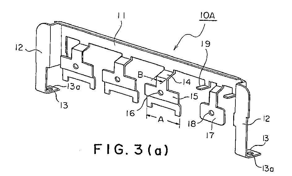
- a fixing plate 10A is mounted.
- the fixing plate 10A includes a base portion 11 that is formed being elongated in a direction in which the devices are arranged, a pair of leg portions 12 for supporting above the printed board 6 the base portion 11 at both longitudinal ends thereof, a foot portions 13 that abut on the device mounting surface, for the leg portions 12, on the printed board 6, three device-pressing portions 15 and a rectifier-pressing portion 17 that are provided being elongated and spaced apart from each other, at one side (the lower side) of the base portion 11 and that are coupled through coupling portions with the base portion; these portions are integrally formed with a metal plate, through bending and forming processing; and the foot portions 13 are fixed to the printed board 6, by upwardly advancing the screws 13b through the printed board 6 and the foot portions 13.
- the rectifier 2 and the switching devices U, X, V, Y, W, and Z are fixed with the screws.
- the heat sink 7 has a mounting trunk portion to which the rectifier 2 and the switching devices U, X, V, Y, W, and Z are adhered and radiating fins situated on the backside of trunk portion.
- the device-pressing portions 15 and the rectifier-pressing portion 17 each have a through-hole for a screw; a screw is passed through the through-hole, and then screwed into a screw hole in the mounting trunk portion of the heat sink 7, thereby being fixed.
- Figs. 3(a) and 3(b) are perspective views illustrating in detail the configuration of the fixing plate 10A;
- Fig. 3(a) illustrate the back side, of the fixing plate 10A, on which the rectifier 2 and the switching devices U, X, V, Y, W, and Z are fixed and which faces the heat sink 7;
- Fig. 3(b) illustrates the front side, of the fixing plate 10A, that is opposite the side where the heat sink 7 is situated.
- the base portion 11 having a bent portion 11a in the top portion thereof and the leg portions 12 that are elongated downwardly from both ends of the base portion 11 are integrally formed; further, the base portion 11 and the three device-pressing portions 15 and the rectifier-pressing portion 17 that are situated under the base portion 11 are integrally formed.
- the leg portion 12 has the foot portion 13 at the bottom end thereof; a through-hole 13a for a screw, for fixing to the printed board 6 the fixing plate 10A, is provided in the foot portion 13.
- the device-pressing portions 15 is formed in a shape having a wide width, i.e., a width A, so that two switching devices, e.g., W and Z can concurrently be pressed with a predetermined spacing; the top end of the device-pressing portions 15 is coupled with the base portion 11, through a coupling portion 14 formed in such a way as to have a small width, i.e., a width B ( ⁇ A).
- the coupling portion 14 is elongated obliquely downward from the base portion 11 and has such a shape that the top end thereof is bent approximately vertically downward; the device-pressing portion 15 is made to be in parallel with the base portion 11; and bending processing is applied to the device-pressing portion 15 in such a way that the device-pressing portion 15 has level differences in accordance with the surface contour of a device.
- a through-hole 16 for a screw is provided at the middle of the longitudinal width thereof and in the vicinity of the coupling portion 14.
- the through-hole 16 for a screw is positioned in the space between a pair of the switching devices that is fixed by means of the device-pressing portion 15.
- the reason why the width B of the coupling portion 14 is made small is that, even though the thicknesses of a pair of the switching devices, e.g., W and Z are different due to manufacturing variation, a twist is caused so that tightening force by a screw is applied to both of the switching devices W and Z, and that, when the thicknesses of a pair of the switching devices W and Z are larger or smaller than those of the other switching devices U to Y, a bend is caused.
- the bottom end of the device-pressing portion 15 has an end-portion shape such that the switching devices U, X, V, Y, W, and Z are pressed without a type-name display portion "N" being covered, thereby enabling identification of the type names of the switching devices U, X, V, Y, W, and Z.
- the rectifier-pressing portion 17 for pressing the rectifier 2 is formed approximately as is the case with the device-pressing portion 15; as illustrated in Fig. 4, the rectifier 2 is fixed through the rectifier-pressing portion 17, by means of a screw that passes through a fixing hole 2A provided at the top center of the rectifier 2.
- each of terminals of the rectifier 2 and the switching devices U, X, V, Y, W, and Z is inserted into a predetermined through-hole formed in the printed board 6, in such a way that the cooling surfaces of the rectifier 2 and the switching devices U, X, V, Y, W, and Z face in the same direction, i.e., outward.
- Fig. 5 is a perspective view schematically illustrating a configuration of a positioning jig 20 for, in soldering these terminals, aligning each of the cooling surfaces on the same plane.
- the positioning jig 20 has a plane portion 21 having in the lower portion thereof level differences in accordance with the contours of the devices; at both ends of the plane portion 21, positioning protrusions 22 are formed, and a plurality of positioning protrusions 23 are interposed between both of the positioning protrusions 22; and the spaces between these positioning protrusions make a rectifier-insertion portion 2S, and device-insertion portions US, XS, VS, YS, WS, and ZS.
- the rectifier 2 and the switching devices U, X, V, Y, W, and Z are inserted into the rectifier-insertion portion 2S of the positioning jig 20 and the device-insertion portions US, XS, VS, YS, WS, and ZS, respectively; the positioning jig 20 is held on the printed board 6; and, in this situation, each terminal is soldered to the printed board 6.
- a mounting trunk portion 71 of the heat sink 7 having radiating fins 72 through 79 is pressed through an insulating sheet 9 against the rear surfaces of the rectifier 2 and the switching devices U, X, V, Y, W, and Z.
- the cooling surfaces of the rectifier 2 and the switching devices U, X, V, Y, W, and Z are adhered to the rectifier-pressing portion 17 of the fixing plate 10A.
- Fig. 8 illustrates a situation in which switching devices having different thicknesses are adhered to the mounting trunk portion 71 of the heat sink 7; for example, it is assumed that the thickness of the switching devices U, W, and Z is t1; X, t2 (> t1); V and Y, t3 (> t2).
- the switching devices V and Y, and W and Z to be fixed as pairs, by means of the device-pressing portion 15, have a large thickness and a small thickness, respectively, in comparison to other pairs; however, because the thicknesses of the switching devices that configure a pair are equal to each other, respective contact surfaces are adhered to the mounting trunk portion 71, simply thanks to a bend of the coupling portion 14.
- switching devices are manufactured in such a way as to have packages of a uniform thickness; however, it is difficult to manufacture switching devices having completely the same size, and some tolerances exist.
- the tolerance is within one mm; however, if this small difference prevents a switching device from being sufficiently adhered to the heat sink 7, the device undergoes thermal destruction; therefore, the device and the heat sink 7 should securely be adhered to each other.
- the insulating sheet 9 is interposed between a device and the heat sink 7; however, because of being a sheet having high heat-transfer efficiency and an extremely small and uniform thickness, the insulating sheet 9 does not adversely affect the adhesiveness between the device and the heat sink 7. Thus, in the foregoing discussion, the explanation for the sheet 9 has been omitted.
- the fixing plate 10A that is a single metal plate to which forming processing has been applied has the base portion 11 formed being elongated in the direction in which the switching devices U, X, V, Y, W, and Z are arranged and three device-pressing portions 15 that are formed at one side of the base portion 11, being coupled through the coupling portions 14 with the base portion 11, and being spaced apart form each other; the device-pressing portions 15 have a large width so that two switching devices as a pair are pressed; in contrast, the coupling portion 14 has a smaller width; therefore, even when there is variation in thickness between the switching devices, when the device-pressing portion 15 is tightened with a screw, the switching devices can be securely be adhered to a heat sink by a single fixing plate.
- switching devices utilized in a three-phase inverter should have the same ratings, e.g., a rated current of 15 A; however, in the case of a switching device having a small rated current, even though the rated current is different form others, the appearance and contour of the switching device are specified in the same way as the other switching devices are, whereby devices having different ratings may be intermingled in a manufacturing site.
- the device-pressing portion 15 has a shape such that the switching devices U, X, V, Y, W, and Z are pressed without type-name display portions "N" being covered, thereby enabling visual inspection of the type names and ratings of the switching devices, even though a plurality of kinds of switching devices made by different manufacturers are employed; thus, erroneous mounting can be prevented.
- Fig. 9 is a perspective view, for explaining Second Embodiment of the present invention, illustrating a shape of a fixing plate 10B having a different configuration from that in First Embodiment.
- Second Embodiment is identical to First Embodiment, except for the fixing plate 10B; therefore, figures and explanations for the constituent elements will be omitted.
- the same constituent elements as those of the fixing plate 10A included in First Embodiment are indicated by the same reference marks, and explanations for them will be omitted.
- the configuration of the fixing plate 10B illustrated in Fig. 9 is differentiated from that of the fixing plate 10A incorporated in First Embodiment by including a protrusion 41 that protrudes toward the device-mounting side, i.e., toward the heat sink, being bent at the middle of the longitudinal width of the device-pressing portion 15, arm portions 42a or 42b that protrude in an elongated form toward the heat sink, being bent at both ends of the longitudinal width of the device-pressing portion 15, and fixing protrusions 43 that are provided inside a pair of the leg portions 12 supporting the base portion 11 at both ends of the longitudinal width thereof and that are inserted into holes (unillustrated) formed in the printed board 6. Functions of what differ from the fixing plate 10A in terms of the configuration will be explained below.
- the devices When a pair of switching devices is fixed being tightened by means of the device-pressing portion 15, the devices may move against each other (left and right, respectively) due to the difference in thickness or the like.
- the protrusion 41 and the arm portions 42a or 42b appropriately position the switching devices; for example, as illustrated in Fig. 10, by making the planar shape of the protrusion 41 triangular, the protrusion 41 applies force to each of the switching devices, thereby each switching device being shifted outward in the direction of longitudinal width of the device-pressing portion 15, when the device-pressing portion 15 is pressed against the switching devices.
- the switching devices are pressed against the arm portions 42a or 42b that are bent toward the switching devices at both ends of the device-pressing portion 15. Accordingly, the positions of switching devices U, X, V, Y, W, and Z are defined; therefore, the devices can be appropriately spaced apart from each other.
- the device-pressing portions 15 should be more spaced apart from each other, because the fixing plate 10B itself is a single metal plate to which bending processing has been applied.
- the arm portions 42b are formed at the top sides thereof; with regard to the device-pressing portions 15 arranged at both sides, among the three device-pressing portions 15, the arm portions 42a are formed at the bottom sides thereof.
- the positions where the arm portions 42a or 42b provided at both sides of the device-pressing portion 15 are situated are at the same height from the printed board 6, for each device-pressing portion 15, and the positions where the arm portions 42a and 42b of neighboring device-pressing portions 15 are situated are at different heights; however, also by making the heights of the arm portions 42a provided at both sides of the device-pressing portion 15 different and making the heights of the arm portions facing each other, of the neighboring device-pressing portions 15 different, the same effect can be obtained.
- the fixing protrusion 43 formed in the vicinity of the leg portion 12 is inserted into a hole in the printed board 6 and soldered to the printed board 6, with the foot portion 13 abutting on the printed board 6; accordingly, an effect is demonstrated in which, before the leg portion 13 is fixed by a screw to the printed board 6, the fixing plate 10B can be positioned.
- Fig. 10 is an explanatory view representing that, as explained with reference to Fig. 8, even though the thicknesses of the switching devices U, W, and Z are t1, the thickness of the switching device X is t2 (> t1), and the thicknesses of the switching devices V and Y are t3 (> t2), each contact surface is adhered to the mounting trunk portion 71, thanks to a twist or a bend of the coupling portion 14, and also illustrating the situation in which the positions of the switching devices U, X, V, Y, W, and Z are each defined by the protrusion 41 and the arm portions 42a or 42b.
- the fixing plate 10B of which is illustrated in Fig. 9 in addition to effects of First Embodiment, other effects can also be obtained in which the switching devices U, X, V, Y, W, and Z are appropriately spaced apart from each other; even though, for that purpose, the arm portions 42a or 42b are provided, because these arm portions are provided at different heights, the longitudinal length of the fixing plate 10B is saved, whereby the width of the printed board 6 does not have to be widened; and, prior to being fixed with a screw, the fixing plate 10B can be positioned, by providing the fixing protrusion 43.
- a heat radiation system can be provided in which, even though there is variation in thickness among six switching devices, all of these devices can securely be adhered to a heat sink, by means of a single fixing plate, i.e., by utilizing a small number of components.
Landscapes
- Engineering & Computer Science (AREA)
- Microelectronics & Electronic Packaging (AREA)
- Physics & Mathematics (AREA)
- Thermal Sciences (AREA)
- Power Engineering (AREA)
- Cooling Or The Like Of Electrical Apparatus (AREA)
- Inverter Devices (AREA)
- Cooling Or The Like Of Semiconductors Or Solid State Devices (AREA)
- Mounting Of Printed Circuit Boards And The Like (AREA)
- Dc-Dc Converters (AREA)
Abstract
Description
Claims (4)
- A heat radiation system comprising a fixing plate for fixing to a heat sink six switching devices arranged in a line on a printed board, wherein the fixing plate is made of a single metal plate to which forming processing has been applied, and has a base portion formed being elongated in a direction in which the switching devices are arranged and three device-pressing portions provided at one side of the base portion, in an elongated form being spaced apart form each other and being coupled through coupling portions with the base portion; wherein the device-pressing portion has a width, in the longitudinal direction of the base portion, for pressing two of the switching devices as a pair, and has a through-hole for a screw, formed in the middle of the longitudinal width thereof, for sandwiching the switching device between the device-pressing portion and the heat sink, and fastening the switching device to the heat sink; and wherein the coupling portion is formed so as to have a width smaller than that of the device-pressing portion so that, when the switching device is sandwiched and the device-pressing portion is fastened to the heat sink, the device-pressing portion can be moved obliquely against the heat sink.
- The heat radiation system according to claim 1, wherein, if it is assumed that a surface, of the switching device, facing the heat sink is a rear surface, the type name of the switching device is displayed on the front surface thereof, and the device-pressing portion has a shape such that the switching device is pressed, without a type-name display portion being covered.
- The heat radiation system according to claim 1 or claim 2, wherein the device-pressing portion includes a protrusion that protrudes toward the heat sink, being bent at the middle of the longitudinal width of the device-pressing portion, arm portions that protrude in an elongated form toward the heat sink, being bent at both ends of the longitudinal width of the device-pressing portion, and wherein the arm portions are provided at a height different from a height of the arm portions of the neighboring device-pressing portion, and the respective switching devices are fit between the protrusion and the arm portion.
- The heat radiation system according to claim 1 to claim 3, wherein the fixing plate includes a pair of leg portions for supporting above the printed board the base portion at both longitudinal ends thereof, and the leg portion includes a foot portion that abuts on a device mounting surface of the printed board and a fixing protrusion that is inserted into a hole formed in the printed board.
Applications Claiming Priority (3)
| Application Number | Priority Date | Filing Date | Title |
|---|---|---|---|
| JP2003082337 | 2003-03-25 | ||
| JP2003082337A JP3790225B2 (en) | 2003-03-25 | 2003-03-25 | Heat dissipation device |
| PCT/JP2004/002618 WO2004086501A1 (en) | 2003-03-25 | 2004-03-03 | Heat radiator |
Publications (1)
| Publication Number | Publication Date |
|---|---|
| EP1608014A1 true EP1608014A1 (en) | 2005-12-21 |
Family
ID=33094916
Family Applications (1)
| Application Number | Title | Priority Date | Filing Date |
|---|---|---|---|
| EP04716770A Withdrawn EP1608014A1 (en) | 2003-03-25 | 2004-03-03 | Heat radiator |
Country Status (8)
| Country | Link |
|---|---|
| EP (1) | EP1608014A1 (en) |
| JP (1) | JP3790225B2 (en) |
| KR (1) | KR100687372B1 (en) |
| CN (1) | CN100373600C (en) |
| AU (1) | AU2004224861B2 (en) |
| BR (1) | BRPI0408460A (en) |
| RU (1) | RU2299496C2 (en) |
| WO (1) | WO2004086501A1 (en) |
Cited By (4)
| Publication number | Priority date | Publication date | Assignee | Title |
|---|---|---|---|---|
| EP1968361A3 (en) * | 2007-03-06 | 2010-07-07 | Funai Electric Co., Ltd. | IC fixing structure |
| US20160149380A1 (en) * | 2014-11-20 | 2016-05-26 | Hamilton Sundstrand Corporation | Power control assembly with vertically mounted power devices |
| US11558967B2 (en) * | 2019-07-10 | 2023-01-17 | Diamond & Zebra Electric Mfg. Co., Ltd. | Electronic equipment and electronic control device |
| US20240333167A1 (en) * | 2023-03-28 | 2024-10-03 | Panasonic Intellectual Property Management Co., Ltd. | Power conversion device, structure of power conversion device, and method of manufacturing power conversion device |
Families Citing this family (12)
| Publication number | Priority date | Publication date | Assignee | Title |
|---|---|---|---|---|
| DE102005050028A1 (en) * | 2005-10-14 | 2007-04-19 | Robert Bosch Gmbh | Electric device, in particular for controlling a motor and / or regenerative electric machine |
| EP1981159A1 (en) * | 2006-01-31 | 2008-10-15 | Toshiba Carrier Corporation | Refrigeration cycle device |
| JPWO2010119546A1 (en) * | 2009-04-16 | 2012-10-22 | 三菱電機株式会社 | Heating part fixing bracket |
| WO2013088642A1 (en) * | 2011-12-13 | 2013-06-20 | 富士電機株式会社 | Power conversion device |
| CN103391703B (en) * | 2012-05-11 | 2017-08-18 | 尼得科控制技术有限公司 | Clamping device |
| CN103712171B (en) * | 2012-09-28 | 2018-04-20 | 海洋王(东莞)照明科技有限公司 | Rectifier bracket and lighting apparatus |
| KR101846307B1 (en) * | 2013-07-08 | 2018-04-09 | 지멘스 악티엔게젤샤프트 | Multilevel converter |
| JP2013214770A (en) * | 2013-07-10 | 2013-10-17 | Mitsubishi Electric Corp | Metal fitting and method for fixing heating component |
| CN104684337B (en) * | 2013-11-26 | 2017-12-22 | 台达电子企业管理(上海)有限公司 | Electronic installation and its assemble method |
| KR101624733B1 (en) * | 2014-09-25 | 2016-06-07 | 프레스토라이트아시아 주식회사 | Motor driving controller having improved radiant heat function |
| WO2021186935A1 (en) * | 2020-03-19 | 2021-09-23 | 富士電機株式会社 | Power conversion device |
| CN115513073B (en) * | 2022-11-23 | 2023-03-07 | 季华实验室 | Power device heat dissipation structure and assembly method thereof |
Family Cites Families (9)
| Publication number | Priority date | Publication date | Assignee | Title |
|---|---|---|---|---|
| JPH0621252Y2 (en) * | 1988-12-02 | 1994-06-01 | 光洋電子工業株式会社 | Semiconductor element mounting device |
| JPH0351891U (en) * | 1989-09-27 | 1991-05-20 | ||
| SU1767712A1 (en) * | 1990-04-18 | 1992-10-07 | Институт Точной Механики И Вычислительной Техники Им.С.А.Лебедева | Radio electronic module |
| JPH05218248A (en) * | 1992-02-03 | 1993-08-27 | Murata Mfg Co Ltd | Structure for fitting hot element of heat radiating plate |
| CN1152428C (en) * | 1995-10-13 | 2004-06-02 | 热合金公司 | Solderable Transistor Clips and Clip and Heat Sink Combos |
| US5960535A (en) * | 1997-10-28 | 1999-10-05 | Hewlett-Packard Company | Heat conductive substrate press-mounted in PC board hole for transferring heat from IC to heat sink |
| JP2002198477A (en) * | 2000-12-25 | 2002-07-12 | Toyota Motor Corp | Semiconductor device |
| US6469898B1 (en) * | 2001-05-21 | 2002-10-22 | Rouchon Industries Inc. | Heat dissipating device |
| US6525941B1 (en) * | 2001-12-27 | 2003-02-25 | Tai-Sol Electronics Co., Ltd. | Heat dissipating device with a pressing member that is rotatable to urge a fan module toward a circuit board |
-
2003
- 2003-03-25 JP JP2003082337A patent/JP3790225B2/en not_active Expired - Fee Related
-
2004
- 2004-03-03 WO PCT/JP2004/002618 patent/WO2004086501A1/en not_active Ceased
- 2004-03-03 CN CNB200480008179XA patent/CN100373600C/en not_active Expired - Fee Related
- 2004-03-03 RU RU2005132829/28A patent/RU2299496C2/en not_active IP Right Cessation
- 2004-03-03 AU AU2004224861A patent/AU2004224861B2/en not_active Ceased
- 2004-03-03 BR BRPI0408460-8A patent/BRPI0408460A/en not_active IP Right Cessation
- 2004-03-03 KR KR1020057017882A patent/KR100687372B1/en not_active Expired - Fee Related
- 2004-03-03 EP EP04716770A patent/EP1608014A1/en not_active Withdrawn
Non-Patent Citations (1)
| Title |
|---|
| See references of WO2004086501A1 * |
Cited By (4)
| Publication number | Priority date | Publication date | Assignee | Title |
|---|---|---|---|---|
| EP1968361A3 (en) * | 2007-03-06 | 2010-07-07 | Funai Electric Co., Ltd. | IC fixing structure |
| US20160149380A1 (en) * | 2014-11-20 | 2016-05-26 | Hamilton Sundstrand Corporation | Power control assembly with vertically mounted power devices |
| US11558967B2 (en) * | 2019-07-10 | 2023-01-17 | Diamond & Zebra Electric Mfg. Co., Ltd. | Electronic equipment and electronic control device |
| US20240333167A1 (en) * | 2023-03-28 | 2024-10-03 | Panasonic Intellectual Property Management Co., Ltd. | Power conversion device, structure of power conversion device, and method of manufacturing power conversion device |
Also Published As
| Publication number | Publication date |
|---|---|
| JP3790225B2 (en) | 2006-06-28 |
| RU2299496C2 (en) | 2007-05-20 |
| AU2004224861B2 (en) | 2007-06-07 |
| CN1765018A (en) | 2006-04-26 |
| CN100373600C (en) | 2008-03-05 |
| KR20050116154A (en) | 2005-12-09 |
| BRPI0408460A (en) | 2006-04-04 |
| KR100687372B1 (en) | 2007-02-26 |
| WO2004086501A1 (en) | 2004-10-07 |
| JP2004289076A (en) | 2004-10-14 |
| RU2005132829A (en) | 2006-02-27 |
| AU2004224861A1 (en) | 2004-10-07 |
Similar Documents
| Publication | Publication Date | Title |
|---|---|---|
| AU2004224861B2 (en) | Heat radiator | |
| US7113405B2 (en) | Integrated power modules with a cooling passageway and methods for forming the same | |
| US7046535B2 (en) | Architecture for power modules such as power inverters | |
| US7292451B2 (en) | Architecture for power modules such as power inverters | |
| AU2006335521B2 (en) | Drive circuit of motor and outdoor unit of air conditioner | |
| US7301755B2 (en) | Architecture for power modules such as power inverters | |
| US7289343B2 (en) | Architecture for power modules such as power inverters | |
| JPH02305498A (en) | Cold plate assembly | |
| CN102598880A (en) | Wiring board unit | |
| JP2007533145A (en) | Power semiconductor circuit | |
| CN109995246A (en) | Switching power unit | |
| US6674164B1 (en) | System for uniformly interconnecting and cooling | |
| JP2003264388A (en) | Electrical component equipment | |
| US9485865B2 (en) | Substrate spacing member and inverter device | |
| US7944711B2 (en) | Discrete electronic component and related assembling method | |
| JP2006339170A (en) | Inverter device and manufacturing method thereof | |
| CN209993589U (en) | IGBT radiator of miniwatt converter | |
| CN223528267U (en) | A heat dissipation structure for an electronic device and the electronic device itself. | |
| JP2000323875A (en) | Equipment and method for cooling electronic component | |
| JP2004022591A (en) | Heat sink mounting structure for board mounted components and method of assembling the same | |
| JP2003031738A (en) | Semiconductor device | |
| JP2025086203A (en) | Electronic component device and method for manufacturing electronic component device | |
| JP2001148556A (en) | Fixing structure of power circuit unit, fixing structure of circuit board, and method for fixing power circuit unit | |
| JPH07307591A (en) | Electronic device heat sink | |
| JPH0714694U (en) | Heat dissipation structure for electronic devices |
Legal Events
| Date | Code | Title | Description |
|---|---|---|---|
| PUAI | Public reference made under article 153(3) epc to a published international application that has entered the european phase |
Free format text: ORIGINAL CODE: 0009012 |
|
| 17P | Request for examination filed |
Effective date: 20050922 |
|
| AK | Designated contracting states |
Kind code of ref document: A1 Designated state(s): AT BE BG CH CY CZ DE DK EE ES FI FR GB GR HU IE IT LI LU MC NL PL PT RO SE SI SK TR |
|
| AX | Request for extension of the european patent |
Extension state: AL LT LV MK |
|
| RIN1 | Information on inventor provided before grant (corrected) |
Inventor name: HASEGAWA, NORIHISA Inventor name: ENDO, TAKAHISA Inventor name: MURASHIGE, YOSHINORI Inventor name: HIRUMA, ATSUYUKI Inventor name: IKEYA, SATOSHI Inventor name: SHIMIZU, SHINYA |
|
| DAX | Request for extension of the european patent (deleted) | ||
| STAA | Information on the status of an ep patent application or granted ep patent |
Free format text: STATUS: THE APPLICATION HAS BEEN WITHDRAWN |
|
| 18W | Application withdrawn |
Effective date: 20081014 |