EP1608011A1 - Heat treatment-purpose wafer support tool, and heat treatment device - Google Patents
Heat treatment-purpose wafer support tool, and heat treatment device Download PDFInfo
- Publication number
- EP1608011A1 EP1608011A1 EP04722467A EP04722467A EP1608011A1 EP 1608011 A1 EP1608011 A1 EP 1608011A1 EP 04722467 A EP04722467 A EP 04722467A EP 04722467 A EP04722467 A EP 04722467A EP 1608011 A1 EP1608011 A1 EP 1608011A1
- Authority
- EP
- European Patent Office
- Prior art keywords
- heat treatment
- wafer
- wafer support
- support tool
- treatment according
- Prior art date
- Legal status (The legal status is an assumption and is not a legal conclusion. Google has not performed a legal analysis and makes no representation as to the accuracy of the status listed.)
- Withdrawn
Links
Images






Classifications
-
- H—ELECTRICITY
- H10—SEMICONDUCTOR DEVICES; ELECTRIC SOLID-STATE DEVICES NOT OTHERWISE PROVIDED FOR
- H10P—GENERIC PROCESSES OR APPARATUS FOR THE MANUFACTURE OR TREATMENT OF DEVICES COVERED BY CLASS H10
- H10P72/00—Handling or holding of wafers, substrates or devices during manufacture or treatment thereof
- H10P72/70—Handling or holding of wafers, substrates or devices during manufacture or treatment thereof for supporting or gripping
- H10P72/76—Handling or holding of wafers, substrates or devices during manufacture or treatment thereof for supporting or gripping using mechanical means, e.g. clamps or pinches
- H10P72/7604—Handling or holding of wafers, substrates or devices during manufacture or treatment thereof for supporting or gripping using mechanical means, e.g. clamps or pinches the wafers being placed on a susceptor, stage or support
- H10P72/7614—Handling or holding of wafers, substrates or devices during manufacture or treatment thereof for supporting or gripping using mechanical means, e.g. clamps or pinches the wafers being placed on a susceptor, stage or support characterised by a plurality of individual support members, e.g. support posts or protrusions
-
- H—ELECTRICITY
- H10—SEMICONDUCTOR DEVICES; ELECTRIC SOLID-STATE DEVICES NOT OTHERWISE PROVIDED FOR
- H10P—GENERIC PROCESSES OR APPARATUS FOR THE MANUFACTURE OR TREATMENT OF DEVICES COVERED BY CLASS H10
- H10P72/00—Handling or holding of wafers, substrates or devices during manufacture or treatment thereof
- H10P72/04—Apparatus for manufacture or treatment
- H10P72/0431—Apparatus for thermal treatment
- H10P72/0434—Apparatus for thermal treatment mainly by convection
-
- H—ELECTRICITY
- H10—SEMICONDUCTOR DEVICES; ELECTRIC SOLID-STATE DEVICES NOT OTHERWISE PROVIDED FOR
- H10P—GENERIC PROCESSES OR APPARATUS FOR THE MANUFACTURE OR TREATMENT OF DEVICES COVERED BY CLASS H10
- H10P72/00—Handling or holding of wafers, substrates or devices during manufacture or treatment thereof
- H10P72/10—Handling or holding of wafers, substrates or devices during manufacture or treatment thereof using carriers specially adapted therefor, e.g. front opening unified pods [FOUP]
- H10P72/12—Vertical boat type carrier whereby the substrates are horizontally supported, e.g. comprising rod-shaped elements
-
- H—ELECTRICITY
- H10—SEMICONDUCTOR DEVICES; ELECTRIC SOLID-STATE DEVICES NOT OTHERWISE PROVIDED FOR
- H10P—GENERIC PROCESSES OR APPARATUS FOR THE MANUFACTURE OR TREATMENT OF DEVICES COVERED BY CLASS H10
- H10P72/00—Handling or holding of wafers, substrates or devices during manufacture or treatment thereof
- H10P72/10—Handling or holding of wafers, substrates or devices during manufacture or treatment thereof using carriers specially adapted therefor, e.g. front opening unified pods [FOUP]
- H10P72/12—Vertical boat type carrier whereby the substrates are horizontally supported, e.g. comprising rod-shaped elements
- H10P72/127—Vertical boat type carrier whereby the substrates are horizontally supported, e.g. comprising rod-shaped elements characterised by the substrate support
-
- H—ELECTRICITY
- H10—SEMICONDUCTOR DEVICES; ELECTRIC SOLID-STATE DEVICES NOT OTHERWISE PROVIDED FOR
- H10P—GENERIC PROCESSES OR APPARATUS FOR THE MANUFACTURE OR TREATMENT OF DEVICES COVERED BY CLASS H10
- H10P72/00—Handling or holding of wafers, substrates or devices during manufacture or treatment thereof
- H10P72/50—Handling or holding of wafers, substrates or devices during manufacture or treatment thereof for positioning, orientation or alignment
-
- H—ELECTRICITY
- H10—SEMICONDUCTOR DEVICES; ELECTRIC SOLID-STATE DEVICES NOT OTHERWISE PROVIDED FOR
- H10P—GENERIC PROCESSES OR APPARATUS FOR THE MANUFACTURE OR TREATMENT OF DEVICES COVERED BY CLASS H10
- H10P72/00—Handling or holding of wafers, substrates or devices during manufacture or treatment thereof
- H10P72/70—Handling or holding of wafers, substrates or devices during manufacture or treatment thereof for supporting or gripping
-
- H—ELECTRICITY
- H10—SEMICONDUCTOR DEVICES; ELECTRIC SOLID-STATE DEVICES NOT OTHERWISE PROVIDED FOR
- H10P—GENERIC PROCESSES OR APPARATUS FOR THE MANUFACTURE OR TREATMENT OF DEVICES COVERED BY CLASS H10
- H10P95/00—Generic processes or apparatus for manufacture or treatments not covered by the other groups of this subclass
- H10P95/90—Thermal treatments, e.g. annealing or sintering
Definitions
- the present invention relates to a wafer support tool used in heat treatment of a wafer such as a semiconductor wafer, for example a silicon wafer, and to a heat treatment apparatus.
- a wafer support tool used for batch type heat treatment there has been generally adopted a design that plural wafers are inserted and held in parallel to one another in grooves of a structure called a boat, which has support poles with the grooves.
- SiC is generally adopted as material of a wafer support tool because of its heat resistance and other properties.
- a method is adopted to cut grooves directly in the support poles with a diamond cutter or the like.
- the batch type heat treatment is to heat treat many wafers at a time using resistance heating (with a heater).
- resistance heating with a heater
- RTP Rapid Thermal Processing
- Examples of heat treatment using an RTP apparatus can include: heat treatment for annihilating defects on a wafer surface, heat treatment for annihilating oxygen donors, heat treatment for producing a shallow diffused layer (RTA: Rapid Thermal Annealing), heat treatment for producing a thin oxide film (RTO: Rapid Thermal Oxidation) or the like.
- RTA Rapid Thermal Annealing
- RTO Rapid Thermal Oxidation
- a wafer support tool (may be called "a susceptor”) for heat treatment is employed; therefore, a problem has remained unsolved that slip dislocations are easy to occur in contact portions of the wafer support tool with a wafer (see JP-A 2002-164300).
- the present invention has been made in order to solve the above problem and it is an object of the present invention to provide a wafer support tool for heat treatment easy in working and capable of realizing reduction in cost without generating damages or slip dislocations that would be otherwise caused by high temperature heat treatment and a heat treatment apparatus.
- a wafer support tool for heat treatment of the present invention comprises: a plurality of wafer support members for supporting a wafer to be heat treated; and a support member holder for holding the wafer support members, wherein the wafer support members each has a contact portion with the wafer, at least one of the contact portions being movable relative to the support member holder.
- a configuration of the contact portion is a curved surface convex against a wafer to be heat treated and especially preferably spherical or ellipsoidal.
- the wafer support member is a pin
- the support member holder is a pin holder for holding the pin and the pin is fitted in a pinhole formed in the pin holder.
- the pin is preferably removable from the pin holder and preferably formed by working a cylindrical body.
- Raw material of the pin and the pin holder can be SiC, silicon or quartz.
- a plurality of pinholes is preferably provided and the pinhole is preferably slit-shaped.
- the slit-shaped pinholes are desirably provided radially from the center of the pin holder.
- the pin holder is preferably disc-shaped or ring-shaped and in a case where the pin holder is disc-shaped, a circular pinhole is formed in the center position thereof.
- the wafer support member may comprise a rotatable body as the contact portion with the wafer to be heat treated, and the rotatable body is accommodated in a rotatable body accommodating hole formed in the wafer support member or the support member holder and rotatable by friction force with the wafer to be heat treated.
- the rotatable body is preferably in the form of a sphere, an ellipsoid, a hollow cylinder or a solid cylinder.
- the rotatable body accommodating hole is desirably in the form of a slit groove and the rotatable body accommodating holes each in the form of a slit groove are preferably formed radially from the center of the support member holder.
- the support member holder is preferably disc-shaped or ring-shaped. Material of the rotatable body may be SiC, silicon or quartz.
- the wafer support tool for heat treatment of the present invention may further comprise: support poles for holding the plural support member holders; and bases for holding the support poles.
- the support member holders may be preferably removable from the support poles.
- Material of the support poles and the bases may be SiC, silicon or quartz.
- a heat treatment apparatus of the present invention has the wafer support tool for heat treat treatment of the present invention.
- reference numeral 10 designates a wafer support tool for heat treatment pertaining to the present invention.
- the wafer support tool 10 includes: a pair of bases 12 and 14 provided opposite each other in a vertical direction; and plural support poles 16 (3 poles in FIG. 2) provided vertically between the bases 12 and 14.
- the upper end and lower end of the support pole 16 are fitted respectively in a receiving hole 18 bored on the lower surface of the upper base 12 and a receiving hole 20 bored on the upper surface of the lower base 14 so that the support pole 16 is removably held with the bases 12 and 14.
- Reference numeral 22 designates a pin as a wafer support member used for supporting a wafer W to be heat treated.
- the pin 22 is, as shown in FIG. 3(b1) or 3(b2), provided with a contact section 26 for supporting a wafer W at the distal end thereof and provided with a fitting portion 28 at the proximal end thereof.
- a shape of the contact section 26 of the pin 22 is preferably a curved surface convex toward the wafer W to be supported.
- FIG. 1, FIG. 2 and FIG. 3(b1) there are shown cases where the shapes of the contact sections 26 are spherical. No specific limitation is imposed on the shape of the contact section 26 and any of shapes other than a sphere can be adopted as far as the shape is, as described above, a curved surface convex toward the wafer W to be supported and the contact section 26 can also be in the shape of an ellipsoid, which is shown in the second embodiment of FIG. 3(b2) and FIG. 7.
- FIG. 7 a difference from FIG. 1 is only the shape of the pin 22 and the repetitive description of the structure is omitted.
- the same symbols are used to the same members as or the members similar to those in FIG. 1.
- Insert grooves 30 are formed on the side surfaces of the support poles 16 at the same heights.
- Reference numeral 32 designates pin holders as support member holders removably supporting the pins 22 and no limitation is imposed on a shape of the pin holders and in FIGs. 2 and 4, there are shown cases of discs.
- the pin holders 32 are inserted into the insert grooves 30 and thereby the pin holders 32 are removably inserted and held in the poles 16.
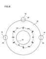
- the pin holders 32 are, as shown in FIGs. 2 and 4, in the shape of a disc and besides, can also be, as shown in Fig. 8, formed in the shape of an annulus with an opening 33 in the central portion.
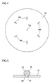
- a circular fitting hole 34a and slit-like fitting holes 34b are, as shown in FIGs. 2 and 4, bored on the disc-like pin holder 32 corresponding to the fitting portions 28 of the pins 22.
- a fitting hole (a pinhole) may be either a through hole or a hole with the bottom. The fitting portion 28 is fitted into the circular fitting hole 34a formed in the central portion of the disc-like pin holder 32 and thereby the pin 22 is removably held by the disc-like pin holder 32.
- the pins 22 fitted in the slit-like fitting holes 34b formed radially from the center of the disc-like pin holder 32 can be moved relative to the disc-like pin holder 32 by a value of the order of several mm in a direction in which a wafer is extended or contracted during a heat treatment process, that is in a direction toward the outer periphery from the center of the disc-like pin holder 32 (FIG. 6(b)) or in a direction opposite it, that is in a direction toward the center (FIG. 6(c)) so as to alleviate stress generated at a contact plane between the pin 22 and the wafer W by a motion of the wafer in the direction in which the wafer is extended or contracted during the heat treatment process.
- the pin 22 can be, as shown in Figs. 3(a), 3(b1) and 3(b2), easily obtained by grinding a pin body 22a in the shape of a cylinder with a lathe and surface roughness of the pin, especially, the contact section 26, can be easily controlled.
- the pin body 22a is made of SiC, Si (single crystal or polycrystal) or quartz in the shape with a diameter of the order in the range of from 1 to 7 mm and a length of the order in the range of from 5 to 10 mm.
- Raw material of the support pole 16 and the bases 12 and 14 may also be preferably SiC, silicon or quartz.
- the circular fitting hole 34a formed in the central portion of the disc-like pin holder 32 shown in Figs. 2 and 4 is in the shape of a circle with a diameter of the order in the range of from 1 to 7 mm and the slit-like fitting holes 34b formed radially from the center of the pin holder 32 are in the shape with a width of the order in the range of from 1 to 7 mm and a length of the order in the range of from 4 to 21 mm.
- the slit-like fitting holes 34b in number of the order in the range of from 3 to 24 sites are arranged radially from the center of the pin holder 32 with length directions of the slits in alignment with radii (6 sites in FIGs. 2 and 4).
- the fitting hole 34a formed at the central portion of the pin holder 32 is naturally omitted but in a case where the pin holder 32 is in the shape of a disc as shown in FIG. 4 as well, the fitting hole 34a may be omitted.
- a wafer support tool of the present invention since the shape of the contact portion of the distal end of the pin with the wafer is formed so as to be curved surface convex toward the wafer, neither damages nor slip dislocations occur at the contact portion with the wafer during heat treatment so that productivity may be improved to achieve cost reduction.
- Surface roughness of the contact portion 26 of the pin 22 with the wafer W may also be adjusted to a desirable value only by additionally working the surface of the contact portion 26.
- positions on the wafer W in contact with the pins 22 in-plane positions on the wafer W
- shapes of the contact portions 26 may be freely designed. In a case where only the pins 22 can be removed from the pin holder 32, cleaning and exchange of the pins may be easy and the surfaces of the pins may also be reworked for recycling.
- the pins are removably held by the pin holder 32 with the fitting hole 34a, 34b; the pin holders 32 are removably held by the support pole 16 with the insert grooves 30; and the support poles 16 are removably held by the bases 12, 14 with the receiving holes 18 and 20.
- another structure may also be adopted in which the pins 22 are irremovably fixed on the pin holder 32, the pin holders 32 are irremovably fixed to the support poles 16 and the support poles 16 are irremovably fixed to the bases 12, 14.
- reference numeral 40 designates a wafer support member holder, which constitutes a wafer support tool for heat treatment according to the present invention.
- the support member holder 40 holds the wafer support members 42.
- the wafer support member 42 has a trapezoidal member 44 arranged on the upper surface of the support member holder 40.
- a rotatable body accommodating hole 46 is bored on the upper surface of the trapezoidal member 44.
- the rotatable body 48 as a contact portion with a wafer W to be heat treated is rotatably fitted in the rotatable body accommodating hole 46.
- An arrow mark 50 shows a given position of the rotatable body 48.
- a shape of the rotatable body 48 No specific limitation is imposed on a shape of the rotatable body 48, and there can be adopted shapes such as a sphere of FIG. 10(a), an ellipsoid of FIG. 10(b) and a hollow cylinder or a solid cylinder of FIG. 10(c) as viewed from above.
- the rotatable body accommodating hole 46 is bored on the upper surface of the trapezoidal member 44, while another construction can be adopted in which the rotatable body accommodating hole 46 is bored directly on the upper surface of the support member holder 40 with omitting the trapezoidal member 44 and the rotatable body 48 is fitted directly into the rotatable body accommodating hole 46. Still another construction may be adopted in which the trapezoidal member 44 may be replaced with a member having another shape different from the trapezoidal one.
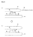
- FIGs. 9(a) and 9(b) there is shown the case where the rotatable body 48 is fitted in the rotatable body accommodating hole 46 on the trapezoidal member 44, while yet another construction can also be adopted in which the shape of the rotatable body accommodating hole 46 is formed in the shape of a slit groove, as shown in FIGs. 11(a) and 11(b) and the rotatable body 48 is accommodated in the slit-like rotatable body accommodating hole 46 so as to be rotatable therein and movable therealong.
- slit groove-like rotatable body accommodating holes 46 are preferably disposed radially from the center of the support member holder 40.
- the slit groove-like rotatable body accommodating hole 46 is bored on the trapezoidal member 44, while a construction can also be adopted in which the slit groove-like rotatable body accommodating hole 46 is bored directly on the upper surface of the support member holder 40 with omitting the trapezoidal member 44 and the rotatable body 48 is accommodated directly in the slit groove-like rotatable body accommodating hole 46 so as to be rotatable therein and movable therealong.
- a heat treatment apparatus of the present invention is a heat treatment apparatus with a wafer support tool for heat treatment of the present invention exemplified in the first to fourth embodiments.
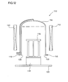
- reference numeral 110 designates a vertical heat treatment furnace.
- the heat treatment furnace 110 comprises: a heater 112 arranged concentrically; a process tube 114 disposed inside thereof; a boat 116 on which plural wafers are placed; a heat insulating cylinder 118 on which the boat 116 is mounted in a freely removable manner; a cover 122 arranged on the lower end of the heat insulating cylinder 118 and closing a furnace opening 120 at the lower end of the process tube 114 during heat treatment; and a vertically moving means not shown moving upward or downward the boat 116, the heat insulating cylinder 118 and the cover 122 toward the interior of the process tube 114.
- Reference numeral 115 is a flange provided at the lower end of the process tube 114.
- FIG. 13 is a descriptive schematic view of an embodiment of the RTP apparatus.
- reference numeral 210 designates a heat treatment apparatus, in other word, an RTP apparatus.
- the heat treatment apparatus 210 has a chamber 211 made from quarts and a wafer W is heat treated in the chamber 211.
- the heat treatment is carried out by heating lamps 212 surrounding the chamber 211 externally, above and below, and left and right. In the heating lamps 212, supply of power can be individually controlled.
- a gas introduction port 219 is provided on the gas introduction side of the chamber 211, while an auto shutter 213 is installed on the gas exhaust side to thereby seal off the outside air.
- a wafer insert port not shown that can be opened or closed with a gate valve is formed in the auto shutter 213.
- a gas exhaust port 220 is formed in the auto shutter 213 so that an atmosphere in the furnace is adjustable.
- the wafer W is placed on a three-point supporter 215 formed on a support tool, for example, a quartz tray 214.
- a buffer 216 made of quarts is provided on the gas introduction port side of the quartz tray 214 and a gas introduced through the gas introduction port 219 can be prevented from blowing directly to the wafer W.
- a special window for measuring a temperature not shown is formed in the chamber 211 and a temperature of the wafer W can be measured with a pyrometer 217 installed outside the chamber 211 through the special window.
- a wafer support tool for heat treatment of the present invention is applied instead of a wafer support tool, for example the quartz tray 214, thereby enabling the RTA apparatus 210 to be used as the heat treatment apparatus of the present invention.
- SiC was used as material of bases, support poles and pins to fabricate a wafer support tool for heat treatment described in FIGs. 1 and 2.
- each of the pins was prepared in a way such that a cylindrical body with a diameter of about 5 mm and a length of 10 mm was used, a contact section in the shape of a sphere with a diameter of about 5 mm was formed at the distal end thereof and a diameter of the proximal end thereof was worked to about 3 mm.
- Six slit-like pinholes provided radially were formed so that the central portions thereof were disposed at positions of 110 mm from the center of the pin holder.
- Such a wafer support tool for heat treatment was used to conduct heat treatment of a CZ silicon single wafer with a diameter of 300 mm, a crystal orientation of ⁇ 100>, a conductivity type of p-type and a resistivity of about 10 ⁇ cm. Investigation was conducted about a state of occurrence of damages or slip dislocations in a contact portion with the wafer.
- Conditions for the heat treatment were in an atmosphere of 100 % argon at 1200°C for 1 hr and the temperature for loading and unloading the wafer was 700°C.
- the heat treated wafer was almost free from occurrence of damages or slip dislocations as a result of investigation with X-ray topography thereabout in the contact portion of the wafer with the wafer support tool.
- SiC was used as material of bases, support poles and pins to fabricate a wafer support tool for heat treatment as described in FIG. 1.
- the pin holder 32 had a diameter of 320 mm and a thickness of 1 mm, and nine slits 34b, each of which was a through hole with a width of 3.5 mm and a length of 9 mm and into each of which a pin was fitted, were formed radially on the pin holder 32, as shown in FIG.
- each of the pins was formed from a cylindrical body having a diameter of 8 mm and a length of 10 mm, and a spherical contact section having a diameter of about 6 mm was formed at the distal end thereof, while the proximal end had a diameter of about 3 mm.
- a total of the nine contact areas between the pins and the wafer were 10 mm 2 or less.
- Such a wafer support tool for heat treatment was used to heat treat a CZ silicon single crystal wafer with a diameter of 300 mm, a crystal orientation of ⁇ 100>, a conductivity type of a p-type and resistivity of about 10 ⁇ cm, followed by investigation about a state of occurrence of slip dislocations in the contact portion with the wafer.
- SIMOX Separatation by Ion-implanted Oxygen
- SOI Silicon On Insulator
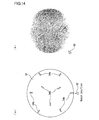
- reference numeral 60 designates an arrow mark indicating a notch position.
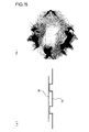
- a conventional wafer holder 70 as shown in FIG. 15(a) (a contact portion of a wafer is in the shape of a ring and a contact area is about 25000 mm 2 ) was used, a wafer W of the same specifications as in Example 2 was used, heat treatment was conducted in the same conditions as in Example 2 and X-ray topography was used to observe slip dislocations thereof, results of which are shown in FIG. 15 (b).
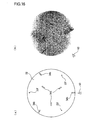
- FIG. 16(a) designates an arrow mark indicating a position of a notch of a wafer.
- the wafer support tool for heat treatment of the present invention has high effectiveness in heat treatment at a high temperature for a long time as in a case of a SIMOX wafer.
- the heat treatment apparatus of the present invention equipped with the above mentioned wafer support tool for heat treatment, there can be provided a wafer with less of damages or slip dislocations after high temperature heat treatment and hence it is possible to improve quality and yield of devices to be fabricated using the wafer.
Landscapes
- Container, Conveyance, Adherence, Positioning, Of Wafer (AREA)
Abstract
Description
Claims (22)
- A wafer support tool for heat treatment comprising:wherein the wafer support members each has a contact portion with the wafer, at least one of the contact portions being movable relative to the support member holder.a plurality of wafer support members for supporting a wafer to be heat treated; anda support member holder for holding the wafer support members,
- The wafer support tool for heat treatment according to claim 1, wherein a configuration of the contact portion is a curved surface convex against the wafer to be heat treated.
- The wafer support tool for heat treatment according to claim 1 or 2, wherein a configuration of the contact portion is spherical or ellipsoidal.
- The wafer support tool for heat treatment according to any of claims 1 to 3, wherein the wafer support member is a pin, the support member holder is a pin holder for holding the pin and the pin is fitted in a pinhole formed in the pin holder.
- The wafer support tool for heat treatment according to claim 4, wherein the pin is removable from the pin holder.
- The wafer support tool for heat treatment according to claim 4 or 5, wherein the pin is formed by working a cylindrical body.
- The wafer support tool for heat treatment according to any of claims 4 to 6, wherein raw material of the pin and the pin holder is SiC, silicon or quartz.
- The wafer support tool for heat treatment according to any of claims 4 to 7, wherein a plurality of pinholes is provided.
- The wafer support tool for heat treatment according to any of claims 4 to 8, wherein the pinhole is slit-shaped.
- The wafer support tool for heat treatment according to claim 9, wherein the slit-shaped pinholes are provided radially from the center of the pin holder.
- The wafer support tool for heat treatment according to any of claims 4 to 10, wherein the pin holder is disc-shaped or ring-shaped.
- The wafer support tool for heat treatment according to claim 11, wherein the pin holder is disc-shaped and a circular pinhole is formed in the center position thereof.
- The wafer support tool for heat treatment according to claim 1 or 2, wherein the wafer support member comprises a rotatable body as the contact portion with the wafer to be heat treated, and the rotatable body is accommodated in a rotatable body accommodating hole formed in the wafer support member or the support member holder and rotatable by friction force with the wafer to be heat treated.
- The wafer support tool for heat treatment according to claim 13, wherein the rotatable body is in the form of a sphere, an ellipsoid, a hollow cylinder or a solid cylinder.
- The wafer support tool for heat treatment according to claim 13 or 14, wherein the rotatable body accommodating hole is in the form of a slit groove.
- The wafer support tool for heat treatment according to claim 15, wherein the rotatable body accommodating holes each in the form of a slit groove are formed radially from the center of the support member holder.
- The wafer support tool for heat treatment according to any of claims 13 to 16, wherein the support member holder is disc-shaped or ring-shaped.
- The wafer support tool for heat treatment according to any of claims 13 to 17, wherein material of the rotatable body is SiC, silicon or quartz.
- The wafer support tool for heat treatment according to any of claims 1 to 18, further comprising: support poles for holding the plural support member holders; and bases for holding the support poles.
- The wafer support tool for heat treatment according to claim 19, wherein the support member holders are removable from the support poles.
- The wafer support tool for heat treatment according to claim 19 or 20, wherein material of the support poles and the bases is SiC, silicon or quartz.
- A heat treatment apparatus having the wafer support tool for heat treatment according to any of claims 1 to 21.
Applications Claiming Priority (3)
| Application Number | Priority Date | Filing Date | Title |
|---|---|---|---|
| JP2003085137 | 2003-03-26 | ||
| JP2003085137 | 2003-03-26 | ||
| PCT/JP2004/003858 WO2004086496A1 (en) | 2003-03-26 | 2004-03-22 | Heat treatment-purpose wafer support tool, and heat treatment device |
Publications (2)
| Publication Number | Publication Date |
|---|---|
| EP1608011A1 true EP1608011A1 (en) | 2005-12-21 |
| EP1608011A4 EP1608011A4 (en) | 2010-07-21 |
Family
ID=33095016
Family Applications (1)
| Application Number | Title | Priority Date | Filing Date |
|---|---|---|---|
| EP04722467A Withdrawn EP1608011A4 (en) | 2003-03-26 | 2004-03-22 | MICROPLATE HOLDER TOOL FOR HEAT TREATMENT PURPOSES, AND THERMAL PROCESSING DEVICE |
Country Status (7)
| Country | Link |
|---|---|
| US (1) | US7393207B2 (en) |
| EP (1) | EP1608011A4 (en) |
| JP (1) | JP4363401B2 (en) |
| KR (1) | KR100877129B1 (en) |
| CN (1) | CN100352032C (en) |
| TW (1) | TW200501306A (en) |
| WO (1) | WO2004086496A1 (en) |
Cited By (1)
| Publication number | Priority date | Publication date | Assignee | Title |
|---|---|---|---|---|
| US8042697B2 (en) | 2008-06-30 | 2011-10-25 | Memc Electronic Materials, Inc. | Low thermal mass semiconductor wafer support |
Families Citing this family (430)
| Publication number | Priority date | Publication date | Assignee | Title |
|---|---|---|---|---|
| US7640267B2 (en) | 2002-11-20 | 2009-12-29 | Radar Networks, Inc. | Methods and systems for managing entities in a computing device using semantic objects |
| JP4935002B2 (en) * | 2005-06-30 | 2012-05-23 | ウシオ電機株式会社 | Heating unit |
| US7564536B2 (en) * | 2005-11-08 | 2009-07-21 | Asml Netherlands B.V. | Lithographic apparatus and device manufacturing method |
| US8454356B2 (en) * | 2006-11-15 | 2013-06-04 | Mattson Technology, Inc. | Systems and methods for supporting a workpiece during heat-treating |
| KR100818842B1 (en) * | 2006-12-27 | 2008-04-01 | 주식회사 실트론 | Wafer support pin and wafer heat treatment method to prevent slip during heat treatment of wafer |
| US7977258B2 (en) * | 2007-04-06 | 2011-07-12 | Mattson Technology, Inc. | Method and system for thermally processing a plurality of wafer-shaped objects |
| TWI393212B (en) * | 2007-07-27 | 2013-04-11 | Han Yang Chen | A wafer stager for thermal treatment |
| KR101405346B1 (en) * | 2008-01-04 | 2014-06-12 | 삼성디스플레이 주식회사 | Substrate pedestal, apparatus for treating substrate having it and the method for aligning substrate |
| JP2009187990A (en) * | 2008-02-01 | 2009-08-20 | Tokyo Electron Ltd | Plasma processing equipment |
| JP5071217B2 (en) * | 2008-04-17 | 2012-11-14 | 信越半導体株式会社 | Vertical heat treatment boat and silicon wafer heat treatment method using the same |
| EP2302998A4 (en) * | 2008-06-20 | 2011-08-31 | Univ Georgia | DEVELOPMENT OF HERBICIDE-RESISTANT HERBICIDE SPECIES |
| US20110214196A1 (en) * | 2008-06-20 | 2011-09-01 | University Of Georgia Research Foundation | Development of herbicide-resistant grass species |
| JP2010027959A (en) * | 2008-07-23 | 2010-02-04 | Sumco Corp | Method for manufacturing high-resistance simox wafer |
| US8186661B2 (en) * | 2008-09-16 | 2012-05-29 | Memc Electronic Materials, Inc. | Wafer holder for supporting a semiconductor wafer during a thermal treatment process |
| US10378106B2 (en) | 2008-11-14 | 2019-08-13 | Asm Ip Holding B.V. | Method of forming insulation film by modified PEALD |
| US9394608B2 (en) | 2009-04-06 | 2016-07-19 | Asm America, Inc. | Semiconductor processing reactor and components thereof |
| US8802201B2 (en) | 2009-08-14 | 2014-08-12 | Asm America, Inc. | Systems and methods for thin-film deposition of metal oxides using excited nitrogen-oxygen species |
| TW201135372A (en) * | 2009-10-20 | 2011-10-16 | Nikon Corp | Substrate supporting apparatus, substrate supporting member, substrate transfer apparatus, exposure apparatus, and device manufacturing method |
| JP5549441B2 (en) * | 2010-01-14 | 2014-07-16 | 東京エレクトロン株式会社 | Holder mechanism, load lock device, processing device, and transport mechanism |
| US9312155B2 (en) | 2011-06-06 | 2016-04-12 | Asm Japan K.K. | High-throughput semiconductor-processing apparatus equipped with multiple dual-chamber modules |
| US9793148B2 (en) | 2011-06-22 | 2017-10-17 | Asm Japan K.K. | Method for positioning wafers in multiple wafer transport |
| US10364496B2 (en) | 2011-06-27 | 2019-07-30 | Asm Ip Holding B.V. | Dual section module having shared and unshared mass flow controllers |
| US10854498B2 (en) * | 2011-07-15 | 2020-12-01 | Asm Ip Holding B.V. | Wafer-supporting device and method for producing same |
| US20130023129A1 (en) | 2011-07-20 | 2013-01-24 | Asm America, Inc. | Pressure transmitter for a semiconductor processing environment |
| US20130067761A1 (en) * | 2011-09-16 | 2013-03-21 | Shenzhen China Star Optoelectronics Technology Co. Ltd. | Drying apparatus |
| US9017481B1 (en) | 2011-10-28 | 2015-04-28 | Asm America, Inc. | Process feed management for semiconductor substrate processing |
| US8946830B2 (en) | 2012-04-04 | 2015-02-03 | Asm Ip Holdings B.V. | Metal oxide protective layer for a semiconductor device |
| US9075266B2 (en) * | 2012-04-19 | 2015-07-07 | Shenzhen China Star Optoelectronics Technology Co., Ltd. | Device for prebaking alignment film by using temperature-controllable pin to support substrate and method thereof |
| KR101354600B1 (en) * | 2012-07-24 | 2014-01-23 | 엘지디스플레이 주식회사 | Improved boat, and heat treatment chamber and apparatus of substrate having the same |
| US9558931B2 (en) | 2012-07-27 | 2017-01-31 | Asm Ip Holding B.V. | System and method for gas-phase sulfur passivation of a semiconductor surface |
| US9659799B2 (en) | 2012-08-28 | 2017-05-23 | Asm Ip Holding B.V. | Systems and methods for dynamic semiconductor process scheduling |
| FR2995394B1 (en) | 2012-09-10 | 2021-03-12 | Soitec Silicon On Insulator | SUPPORT DEVICE FOR A PLURALITY OF SUBSTRATES FOR A VERTICAL OVEN |
| US9021985B2 (en) | 2012-09-12 | 2015-05-05 | Asm Ip Holdings B.V. | Process gas management for an inductively-coupled plasma deposition reactor |
| US9324811B2 (en) | 2012-09-26 | 2016-04-26 | Asm Ip Holding B.V. | Structures and devices including a tensile-stressed silicon arsenic layer and methods of forming same |
| US10714315B2 (en) | 2012-10-12 | 2020-07-14 | Asm Ip Holdings B.V. | Semiconductor reaction chamber showerhead |
| US9640416B2 (en) | 2012-12-26 | 2017-05-02 | Asm Ip Holding B.V. | Single-and dual-chamber module-attachable wafer-handling chamber |
| US20160376700A1 (en) | 2013-02-01 | 2016-12-29 | Asm Ip Holding B.V. | System for treatment of deposition reactor |
| US9484191B2 (en) | 2013-03-08 | 2016-11-01 | Asm Ip Holding B.V. | Pulsed remote plasma method and system |
| US9589770B2 (en) | 2013-03-08 | 2017-03-07 | Asm Ip Holding B.V. | Method and systems for in-situ formation of intermediate reactive species |
| US8993054B2 (en) | 2013-07-12 | 2015-03-31 | Asm Ip Holding B.V. | Method and system to reduce outgassing in a reaction chamber |
| US9018111B2 (en) | 2013-07-22 | 2015-04-28 | Asm Ip Holding B.V. | Semiconductor reaction chamber with plasma capabilities |
| US9793115B2 (en) | 2013-08-14 | 2017-10-17 | Asm Ip Holding B.V. | Structures and devices including germanium-tin films and methods of forming same |
| US9240412B2 (en) | 2013-09-27 | 2016-01-19 | Asm Ip Holding B.V. | Semiconductor structure and device and methods of forming same using selective epitaxial process |
| US9556516B2 (en) | 2013-10-09 | 2017-01-31 | ASM IP Holding B.V | Method for forming Ti-containing film by PEALD using TDMAT or TDEAT |
| US10179947B2 (en) | 2013-11-26 | 2019-01-15 | Asm Ip Holding B.V. | Method for forming conformal nitrided, oxidized, or carbonized dielectric film by atomic layer deposition |
| JP6086056B2 (en) * | 2013-11-26 | 2017-03-01 | 信越半導体株式会社 | Heat treatment method |
| US10683571B2 (en) | 2014-02-25 | 2020-06-16 | Asm Ip Holding B.V. | Gas supply manifold and method of supplying gases to chamber using same |
| US10167557B2 (en) | 2014-03-18 | 2019-01-01 | Asm Ip Holding B.V. | Gas distribution system, reactor including the system, and methods of using the same |
| US9447498B2 (en) | 2014-03-18 | 2016-09-20 | Asm Ip Holding B.V. | Method for performing uniform processing in gas system-sharing multiple reaction chambers |
| US11015245B2 (en) | 2014-03-19 | 2021-05-25 | Asm Ip Holding B.V. | Gas-phase reactor and system having exhaust plenum and components thereof |
| US9404587B2 (en) | 2014-04-24 | 2016-08-02 | ASM IP Holding B.V | Lockout tagout for semiconductor vacuum valve |
| US10858737B2 (en) | 2014-07-28 | 2020-12-08 | Asm Ip Holding B.V. | Showerhead assembly and components thereof |
| US9543180B2 (en) | 2014-08-01 | 2017-01-10 | Asm Ip Holding B.V. | Apparatus and method for transporting wafers between wafer carrier and process tool under vacuum |
| US9890456B2 (en) | 2014-08-21 | 2018-02-13 | Asm Ip Holding B.V. | Method and system for in situ formation of gas-phase compounds |
| US10941490B2 (en) | 2014-10-07 | 2021-03-09 | Asm Ip Holding B.V. | Multiple temperature range susceptor, assembly, reactor and system including the susceptor, and methods of using the same |
| US9657845B2 (en) | 2014-10-07 | 2017-05-23 | Asm Ip Holding B.V. | Variable conductance gas distribution apparatus and method |
| KR102300403B1 (en) | 2014-11-19 | 2021-09-09 | 에이에스엠 아이피 홀딩 비.브이. | Method of depositing thin film |
| KR102263121B1 (en) | 2014-12-22 | 2021-06-09 | 에이에스엠 아이피 홀딩 비.브이. | Semiconductor device and manufacuring method thereof |
| US9478415B2 (en) | 2015-02-13 | 2016-10-25 | Asm Ip Holding B.V. | Method for forming film having low resistance and shallow junction depth |
| US10529542B2 (en) | 2015-03-11 | 2020-01-07 | Asm Ip Holdings B.V. | Cross-flow reactor and method |
| US10276355B2 (en) | 2015-03-12 | 2019-04-30 | Asm Ip Holding B.V. | Multi-zone reactor, system including the reactor, and method of using the same |
| US10458018B2 (en) | 2015-06-26 | 2019-10-29 | Asm Ip Holding B.V. | Structures including metal carbide material, devices including the structures, and methods of forming same |
| US10600673B2 (en) | 2015-07-07 | 2020-03-24 | Asm Ip Holding B.V. | Magnetic susceptor to baseplate seal |
| US10043661B2 (en) | 2015-07-13 | 2018-08-07 | Asm Ip Holding B.V. | Method for protecting layer by forming hydrocarbon-based extremely thin film |
| US9899291B2 (en) | 2015-07-13 | 2018-02-20 | Asm Ip Holding B.V. | Method for protecting layer by forming hydrocarbon-based extremely thin film |
| US10083836B2 (en) | 2015-07-24 | 2018-09-25 | Asm Ip Holding B.V. | Formation of boron-doped titanium metal films with high work function |
| CN105140169B (en) * | 2015-07-29 | 2018-10-19 | 深圳市华星光电技术有限公司 | A kind of support construction and vacuum equipment |
| KR102386998B1 (en) * | 2015-07-30 | 2022-04-15 | 엘지디스플레이 주식회사 | Supporter Pin And Heat Treatment Apparatus Comprising The Same |
| US10087525B2 (en) | 2015-08-04 | 2018-10-02 | Asm Ip Holding B.V. | Variable gap hard stop design |
| US9647114B2 (en) | 2015-08-14 | 2017-05-09 | Asm Ip Holding B.V. | Methods of forming highly p-type doped germanium tin films and structures and devices including the films |
| US9711345B2 (en) | 2015-08-25 | 2017-07-18 | Asm Ip Holding B.V. | Method for forming aluminum nitride-based film by PEALD |
| US9960072B2 (en) | 2015-09-29 | 2018-05-01 | Asm Ip Holding B.V. | Variable adjustment for precise matching of multiple chamber cavity housings |
| US9909214B2 (en) | 2015-10-15 | 2018-03-06 | Asm Ip Holding B.V. | Method for depositing dielectric film in trenches by PEALD |
| US10211308B2 (en) | 2015-10-21 | 2019-02-19 | Asm Ip Holding B.V. | NbMC layers |
| US10072892B2 (en) * | 2015-10-26 | 2018-09-11 | Globalwafers Co., Ltd. | Semiconductor wafer support ring for heat treatment |
| US10322384B2 (en) | 2015-11-09 | 2019-06-18 | Asm Ip Holding B.V. | Counter flow mixer for process chamber |
| US9455138B1 (en) | 2015-11-10 | 2016-09-27 | Asm Ip Holding B.V. | Method for forming dielectric film in trenches by PEALD using H-containing gas |
| US9905420B2 (en) | 2015-12-01 | 2018-02-27 | Asm Ip Holding B.V. | Methods of forming silicon germanium tin films and structures and devices including the films |
| US9607837B1 (en) | 2015-12-21 | 2017-03-28 | Asm Ip Holding B.V. | Method for forming silicon oxide cap layer for solid state diffusion process |
| US9735024B2 (en) | 2015-12-28 | 2017-08-15 | Asm Ip Holding B.V. | Method of atomic layer etching using functional group-containing fluorocarbon |
| US9627221B1 (en) | 2015-12-28 | 2017-04-18 | Asm Ip Holding B.V. | Continuous process incorporating atomic layer etching |
| US11139308B2 (en) | 2015-12-29 | 2021-10-05 | Asm Ip Holding B.V. | Atomic layer deposition of III-V compounds to form V-NAND devices |
| KR102093825B1 (en) * | 2015-12-30 | 2020-03-27 | 맷슨 테크놀로지, 인크. | Substrate support in millisecond annealing system |
| JP6637321B2 (en) * | 2016-02-03 | 2020-01-29 | 株式会社Screenホールディングス | Susceptor and heat treatment equipment for heat treatment |
| US10468251B2 (en) | 2016-02-19 | 2019-11-05 | Asm Ip Holding B.V. | Method for forming spacers using silicon nitride film for spacer-defined multiple patterning |
| US10529554B2 (en) | 2016-02-19 | 2020-01-07 | Asm Ip Holding B.V. | Method for forming silicon nitride film selectively on sidewalls or flat surfaces of trenches |
| US9754779B1 (en) | 2016-02-19 | 2017-09-05 | Asm Ip Holding B.V. | Method for forming silicon nitride film selectively on sidewalls or flat surfaces of trenches |
| US10501866B2 (en) | 2016-03-09 | 2019-12-10 | Asm Ip Holding B.V. | Gas distribution apparatus for improved film uniformity in an epitaxial system |
| US10343920B2 (en) | 2016-03-18 | 2019-07-09 | Asm Ip Holding B.V. | Aligned carbon nanotubes |
| US11319624B2 (en) * | 2016-03-23 | 2022-05-03 | Hon Hai Precision Industry Co., Ltd. | Vapor deposition apparatus, vapor deposition method, and method for manufacturing organic EL display apparatus |
| US9892913B2 (en) | 2016-03-24 | 2018-02-13 | Asm Ip Holding B.V. | Radial and thickness control via biased multi-port injection settings |
| US10087522B2 (en) | 2016-04-21 | 2018-10-02 | Asm Ip Holding B.V. | Deposition of metal borides |
| US10190213B2 (en) | 2016-04-21 | 2019-01-29 | Asm Ip Holding B.V. | Deposition of metal borides |
| US10865475B2 (en) | 2016-04-21 | 2020-12-15 | Asm Ip Holding B.V. | Deposition of metal borides and silicides |
| US10032628B2 (en) | 2016-05-02 | 2018-07-24 | Asm Ip Holding B.V. | Source/drain performance through conformal solid state doping |
| US10367080B2 (en) | 2016-05-02 | 2019-07-30 | Asm Ip Holding B.V. | Method of forming a germanium oxynitride film |
| KR102592471B1 (en) | 2016-05-17 | 2023-10-20 | 에이에스엠 아이피 홀딩 비.브이. | Method of forming metal interconnection and method of fabricating semiconductor device using the same |
| US11453943B2 (en) | 2016-05-25 | 2022-09-27 | Asm Ip Holding B.V. | Method for forming carbon-containing silicon/metal oxide or nitride film by ALD using silicon precursor and hydrocarbon precursor |
| US10388509B2 (en) | 2016-06-28 | 2019-08-20 | Asm Ip Holding B.V. | Formation of epitaxial layers via dislocation filtering |
| US9859151B1 (en) | 2016-07-08 | 2018-01-02 | Asm Ip Holding B.V. | Selective film deposition method to form air gaps |
| US10612137B2 (en) | 2016-07-08 | 2020-04-07 | Asm Ip Holdings B.V. | Organic reactants for atomic layer deposition |
| US9793135B1 (en) | 2016-07-14 | 2017-10-17 | ASM IP Holding B.V | Method of cyclic dry etching using etchant film |
| US10714385B2 (en) | 2016-07-19 | 2020-07-14 | Asm Ip Holding B.V. | Selective deposition of tungsten |
| KR102354490B1 (en) | 2016-07-27 | 2022-01-21 | 에이에스엠 아이피 홀딩 비.브이. | Method of processing a substrate |
| KR102532607B1 (en) | 2016-07-28 | 2023-05-15 | 에이에스엠 아이피 홀딩 비.브이. | Substrate processing apparatus and method of operating the same |
| US10177025B2 (en) | 2016-07-28 | 2019-01-08 | Asm Ip Holding B.V. | Method and apparatus for filling a gap |
| US10395919B2 (en) | 2016-07-28 | 2019-08-27 | Asm Ip Holding B.V. | Method and apparatus for filling a gap |
| US9887082B1 (en) | 2016-07-28 | 2018-02-06 | Asm Ip Holding B.V. | Method and apparatus for filling a gap |
| US9812320B1 (en) | 2016-07-28 | 2017-11-07 | Asm Ip Holding B.V. | Method and apparatus for filling a gap |
| US10090316B2 (en) | 2016-09-01 | 2018-10-02 | Asm Ip Holding B.V. | 3D stacked multilayer semiconductor memory using doped select transistor channel |
| US10410943B2 (en) | 2016-10-13 | 2019-09-10 | Asm Ip Holding B.V. | Method for passivating a surface of a semiconductor and related systems |
| US10643826B2 (en) | 2016-10-26 | 2020-05-05 | Asm Ip Holdings B.V. | Methods for thermally calibrating reaction chambers |
| US11532757B2 (en) | 2016-10-27 | 2022-12-20 | Asm Ip Holding B.V. | Deposition of charge trapping layers |
| US10435790B2 (en) | 2016-11-01 | 2019-10-08 | Asm Ip Holding B.V. | Method of subatmospheric plasma-enhanced ALD using capacitively coupled electrodes with narrow gap |
| US10229833B2 (en) | 2016-11-01 | 2019-03-12 | Asm Ip Holding B.V. | Methods for forming a transition metal nitride film on a substrate by atomic layer deposition and related semiconductor device structures |
| US10643904B2 (en) | 2016-11-01 | 2020-05-05 | Asm Ip Holdings B.V. | Methods for forming a semiconductor device and related semiconductor device structures |
| US10714350B2 (en) | 2016-11-01 | 2020-07-14 | ASM IP Holdings, B.V. | Methods for forming a transition metal niobium nitride film on a substrate by atomic layer deposition and related semiconductor device structures |
| US10134757B2 (en) | 2016-11-07 | 2018-11-20 | Asm Ip Holding B.V. | Method of processing a substrate and a device manufactured by using the method |
| KR102546317B1 (en) | 2016-11-15 | 2023-06-21 | 에이에스엠 아이피 홀딩 비.브이. | Gas supply unit and substrate processing apparatus including the same |
| US10340135B2 (en) | 2016-11-28 | 2019-07-02 | Asm Ip Holding B.V. | Method of topologically restricted plasma-enhanced cyclic deposition of silicon or metal nitride |
| KR102762543B1 (en) | 2016-12-14 | 2025-02-05 | 에이에스엠 아이피 홀딩 비.브이. | Substrate processing apparatus |
| US9916980B1 (en) | 2016-12-15 | 2018-03-13 | Asm Ip Holding B.V. | Method of forming a structure on a substrate |
| US11447861B2 (en) | 2016-12-15 | 2022-09-20 | Asm Ip Holding B.V. | Sequential infiltration synthesis apparatus and a method of forming a patterned structure |
| US11581186B2 (en) | 2016-12-15 | 2023-02-14 | Asm Ip Holding B.V. | Sequential infiltration synthesis apparatus |
| KR102700194B1 (en) | 2016-12-19 | 2024-08-28 | 에이에스엠 아이피 홀딩 비.브이. | Substrate processing apparatus |
| US10269558B2 (en) | 2016-12-22 | 2019-04-23 | Asm Ip Holding B.V. | Method of forming a structure on a substrate |
| US10867788B2 (en) | 2016-12-28 | 2020-12-15 | Asm Ip Holding B.V. | Method of forming a structure on a substrate |
| US11390950B2 (en) | 2017-01-10 | 2022-07-19 | Asm Ip Holding B.V. | Reactor system and method to reduce residue buildup during a film deposition process |
| US10655221B2 (en) | 2017-02-09 | 2020-05-19 | Asm Ip Holding B.V. | Method for depositing oxide film by thermal ALD and PEALD |
| US10468261B2 (en) | 2017-02-15 | 2019-11-05 | Asm Ip Holding B.V. | Methods for forming a metallic film on a substrate by cyclical deposition and related semiconductor device structures |
| US10529563B2 (en) | 2017-03-29 | 2020-01-07 | Asm Ip Holdings B.V. | Method for forming doped metal oxide films on a substrate by cyclical deposition and related semiconductor device structures |
| US10283353B2 (en) | 2017-03-29 | 2019-05-07 | Asm Ip Holding B.V. | Method of reforming insulating film deposited on substrate with recess pattern |
| US10103040B1 (en) | 2017-03-31 | 2018-10-16 | Asm Ip Holding B.V. | Apparatus and method for manufacturing a semiconductor device |
| USD830981S1 (en) | 2017-04-07 | 2018-10-16 | Asm Ip Holding B.V. | Susceptor for semiconductor substrate processing apparatus |
| KR102457289B1 (en) | 2017-04-25 | 2022-10-21 | 에이에스엠 아이피 홀딩 비.브이. | Method for depositing a thin film and manufacturing a semiconductor device |
| US10770286B2 (en) | 2017-05-08 | 2020-09-08 | Asm Ip Holdings B.V. | Methods for selectively forming a silicon nitride film on a substrate and related semiconductor device structures |
| US10892156B2 (en) | 2017-05-08 | 2021-01-12 | Asm Ip Holding B.V. | Methods for forming a silicon nitride film on a substrate and related semiconductor device structures |
| US10446393B2 (en) | 2017-05-08 | 2019-10-15 | Asm Ip Holding B.V. | Methods for forming silicon-containing epitaxial layers and related semiconductor device structures |
| US10504742B2 (en) | 2017-05-31 | 2019-12-10 | Asm Ip Holding B.V. | Method of atomic layer etching using hydrogen plasma |
| US10886123B2 (en) | 2017-06-02 | 2021-01-05 | Asm Ip Holding B.V. | Methods for forming low temperature semiconductor layers and related semiconductor device structures |
| US12040200B2 (en) | 2017-06-20 | 2024-07-16 | Asm Ip Holding B.V. | Semiconductor processing apparatus and methods for calibrating a semiconductor processing apparatus |
| US11306395B2 (en) | 2017-06-28 | 2022-04-19 | Asm Ip Holding B.V. | Methods for depositing a transition metal nitride film on a substrate by atomic layer deposition and related deposition apparatus |
| US10685834B2 (en) | 2017-07-05 | 2020-06-16 | Asm Ip Holdings B.V. | Methods for forming a silicon germanium tin layer and related semiconductor device structures |
| KR20190009245A (en) | 2017-07-18 | 2019-01-28 | 에이에스엠 아이피 홀딩 비.브이. | Methods for forming a semiconductor device structure and related semiconductor device structures |
| US11374112B2 (en) | 2017-07-19 | 2022-06-28 | Asm Ip Holding B.V. | Method for depositing a group IV semiconductor and related semiconductor device structures |
| US12027407B2 (en) * | 2017-07-19 | 2024-07-02 | Taiwan Semiconductor Manufacturing Company, Ltd. | Substrate support apparatus and method |
| US11018002B2 (en) | 2017-07-19 | 2021-05-25 | Asm Ip Holding B.V. | Method for selectively depositing a Group IV semiconductor and related semiconductor device structures |
| US10541333B2 (en) | 2017-07-19 | 2020-01-21 | Asm Ip Holding B.V. | Method for depositing a group IV semiconductor and related semiconductor device structures |
| US10312055B2 (en) | 2017-07-26 | 2019-06-04 | Asm Ip Holding B.V. | Method of depositing film by PEALD using negative bias |
| US10605530B2 (en) | 2017-07-26 | 2020-03-31 | Asm Ip Holding B.V. | Assembly of a liner and a flange for a vertical furnace as well as the liner and the vertical furnace |
| US10590535B2 (en) | 2017-07-26 | 2020-03-17 | Asm Ip Holdings B.V. | Chemical treatment, deposition and/or infiltration apparatus and method for using the same |
| TWI815813B (en) | 2017-08-04 | 2023-09-21 | 荷蘭商Asm智慧財產控股公司 | Showerhead assembly for distributing a gas within a reaction chamber |
| US10692741B2 (en) | 2017-08-08 | 2020-06-23 | Asm Ip Holdings B.V. | Radiation shield |
| US10770336B2 (en) | 2017-08-08 | 2020-09-08 | Asm Ip Holding B.V. | Substrate lift mechanism and reactor including same |
| US10249524B2 (en) | 2017-08-09 | 2019-04-02 | Asm Ip Holding B.V. | Cassette holder assembly for a substrate cassette and holding member for use in such assembly |
| US11139191B2 (en) | 2017-08-09 | 2021-10-05 | Asm Ip Holding B.V. | Storage apparatus for storing cassettes for substrates and processing apparatus equipped therewith |
| US11769682B2 (en) | 2017-08-09 | 2023-09-26 | Asm Ip Holding B.V. | Storage apparatus for storing cassettes for substrates and processing apparatus equipped therewith |
| US10236177B1 (en) | 2017-08-22 | 2019-03-19 | ASM IP Holding B.V.. | Methods for depositing a doped germanium tin semiconductor and related semiconductor device structures |
| USD900036S1 (en) | 2017-08-24 | 2020-10-27 | Asm Ip Holding B.V. | Heater electrical connector and adapter |
| US11830730B2 (en) | 2017-08-29 | 2023-11-28 | Asm Ip Holding B.V. | Layer forming method and apparatus |
| KR102491945B1 (en) | 2017-08-30 | 2023-01-26 | 에이에스엠 아이피 홀딩 비.브이. | Substrate processing apparatus |
| US11295980B2 (en) | 2017-08-30 | 2022-04-05 | Asm Ip Holding B.V. | Methods for depositing a molybdenum metal film over a dielectric surface of a substrate by a cyclical deposition process and related semiconductor device structures |
| US11056344B2 (en) | 2017-08-30 | 2021-07-06 | Asm Ip Holding B.V. | Layer forming method |
| KR102401446B1 (en) | 2017-08-31 | 2022-05-24 | 에이에스엠 아이피 홀딩 비.브이. | Substrate processing apparatus |
| US10607895B2 (en) | 2017-09-18 | 2020-03-31 | Asm Ip Holdings B.V. | Method for forming a semiconductor device structure comprising a gate fill metal |
| KR102630301B1 (en) | 2017-09-21 | 2024-01-29 | 에이에스엠 아이피 홀딩 비.브이. | Method of sequential infiltration synthesis treatment of infiltrateable material and structures and devices formed using same |
| US10844484B2 (en) | 2017-09-22 | 2020-11-24 | Asm Ip Holding B.V. | Apparatus for dispensing a vapor phase reactant to a reaction chamber and related methods |
| US10658205B2 (en) | 2017-09-28 | 2020-05-19 | Asm Ip Holdings B.V. | Chemical dispensing apparatus and methods for dispensing a chemical to a reaction chamber |
| US10403504B2 (en) | 2017-10-05 | 2019-09-03 | Asm Ip Holding B.V. | Method for selectively depositing a metallic film on a substrate |
| US10319588B2 (en) | 2017-10-10 | 2019-06-11 | Asm Ip Holding B.V. | Method for depositing a metal chalcogenide on a substrate by cyclical deposition |
| US10923344B2 (en) | 2017-10-30 | 2021-02-16 | Asm Ip Holding B.V. | Methods for forming a semiconductor structure and related semiconductor structures |
| US10910262B2 (en) | 2017-11-16 | 2021-02-02 | Asm Ip Holding B.V. | Method of selectively depositing a capping layer structure on a semiconductor device structure |
| KR102443047B1 (en) | 2017-11-16 | 2022-09-14 | 에이에스엠 아이피 홀딩 비.브이. | Substrate processing apparatus method and apparatus manufactured thereby |
| US11022879B2 (en) | 2017-11-24 | 2021-06-01 | Asm Ip Holding B.V. | Method of forming an enhanced unexposed photoresist layer |
| CN111316417B (en) | 2017-11-27 | 2023-12-22 | 阿斯莫Ip控股公司 | Storage device for use with batch furnaces for storing wafer cassettes |
| JP7206265B2 (en) | 2017-11-27 | 2023-01-17 | エーエスエム アイピー ホールディング ビー.ブイ. | Equipment with a clean mini-environment |
| US10290508B1 (en) | 2017-12-05 | 2019-05-14 | Asm Ip Holding B.V. | Method for forming vertical spacers for spacer-defined patterning |
| US10872771B2 (en) | 2018-01-16 | 2020-12-22 | Asm Ip Holding B. V. | Method for depositing a material film on a substrate within a reaction chamber by a cyclical deposition process and related device structures |
| CN111630203A (en) | 2018-01-19 | 2020-09-04 | Asm Ip私人控股有限公司 | Method of depositing a gap fill layer by plasma assisted deposition |
| TWI799494B (en) | 2018-01-19 | 2023-04-21 | 荷蘭商Asm 智慧財產控股公司 | Deposition method |
| USD903477S1 (en) | 2018-01-24 | 2020-12-01 | Asm Ip Holdings B.V. | Metal clamp |
| US11018047B2 (en) | 2018-01-25 | 2021-05-25 | Asm Ip Holding B.V. | Hybrid lift pin |
| US10535516B2 (en) | 2018-02-01 | 2020-01-14 | Asm Ip Holdings B.V. | Method for depositing a semiconductor structure on a surface of a substrate and related semiconductor structures |
| USD880437S1 (en) | 2018-02-01 | 2020-04-07 | Asm Ip Holding B.V. | Gas supply plate for semiconductor manufacturing apparatus |
| US11081345B2 (en) | 2018-02-06 | 2021-08-03 | Asm Ip Holding B.V. | Method of post-deposition treatment for silicon oxide film |
| US10896820B2 (en) | 2018-02-14 | 2021-01-19 | Asm Ip Holding B.V. | Method for depositing a ruthenium-containing film on a substrate by a cyclical deposition process |
| JP7124098B2 (en) | 2018-02-14 | 2022-08-23 | エーエスエム・アイピー・ホールディング・ベー・フェー | Method for depositing a ruthenium-containing film on a substrate by a cyclical deposition process |
| US10731249B2 (en) | 2018-02-15 | 2020-08-04 | Asm Ip Holding B.V. | Method of forming a transition metal containing film on a substrate by a cyclical deposition process, a method for supplying a transition metal halide compound to a reaction chamber, and related vapor deposition apparatus |
| US10658181B2 (en) | 2018-02-20 | 2020-05-19 | Asm Ip Holding B.V. | Method of spacer-defined direct patterning in semiconductor fabrication |
| KR102636427B1 (en) | 2018-02-20 | 2024-02-13 | 에이에스엠 아이피 홀딩 비.브이. | Substrate processing method and apparatus |
| US10975470B2 (en) | 2018-02-23 | 2021-04-13 | Asm Ip Holding B.V. | Apparatus for detecting or monitoring for a chemical precursor in a high temperature environment |
| US11473195B2 (en) | 2018-03-01 | 2022-10-18 | Asm Ip Holding B.V. | Semiconductor processing apparatus and a method for processing a substrate |
| US11629406B2 (en) | 2018-03-09 | 2023-04-18 | Asm Ip Holding B.V. | Semiconductor processing apparatus comprising one or more pyrometers for measuring a temperature of a substrate during transfer of the substrate |
| US11114283B2 (en) | 2018-03-16 | 2021-09-07 | Asm Ip Holding B.V. | Reactor, system including the reactor, and methods of manufacturing and using same |
| KR102646467B1 (en) | 2018-03-27 | 2024-03-11 | 에이에스엠 아이피 홀딩 비.브이. | Method of forming an electrode on a substrate and a semiconductor device structure including an electrode |
| US11230766B2 (en) | 2018-03-29 | 2022-01-25 | Asm Ip Holding B.V. | Substrate processing apparatus and method |
| US10510536B2 (en) | 2018-03-29 | 2019-12-17 | Asm Ip Holding B.V. | Method of depositing a co-doped polysilicon film on a surface of a substrate within a reaction chamber |
| US11088002B2 (en) | 2018-03-29 | 2021-08-10 | Asm Ip Holding B.V. | Substrate rack and a substrate processing system and method |
| KR102501472B1 (en) | 2018-03-30 | 2023-02-20 | 에이에스엠 아이피 홀딩 비.브이. | Substrate processing method |
| KR102600229B1 (en) | 2018-04-09 | 2023-11-10 | 에이에스엠 아이피 홀딩 비.브이. | Substrate supporting device, substrate processing apparatus including the same and substrate processing method |
| US12025484B2 (en) | 2018-05-08 | 2024-07-02 | Asm Ip Holding B.V. | Thin film forming method |
| KR102709511B1 (en) | 2018-05-08 | 2024-09-24 | 에이에스엠 아이피 홀딩 비.브이. | Methods for depositing an oxide film on a substrate by a cyclical deposition process and related device structures |
| US12272527B2 (en) | 2018-05-09 | 2025-04-08 | Asm Ip Holding B.V. | Apparatus for use with hydrogen radicals and method of using same |
| TWI816783B (en) | 2018-05-11 | 2023-10-01 | 荷蘭商Asm 智慧財產控股公司 | Methods for forming a doped metal carbide film on a substrate and related semiconductor device structures |
| KR102596988B1 (en) | 2018-05-28 | 2023-10-31 | 에이에스엠 아이피 홀딩 비.브이. | Method of processing a substrate and a device manufactured by the same |
| US11718913B2 (en) | 2018-06-04 | 2023-08-08 | Asm Ip Holding B.V. | Gas distribution system and reactor system including same |
| TWI840362B (en) | 2018-06-04 | 2024-05-01 | 荷蘭商Asm Ip私人控股有限公司 | Wafer handling chamber with moisture reduction |
| US11286562B2 (en) | 2018-06-08 | 2022-03-29 | Asm Ip Holding B.V. | Gas-phase chemical reactor and method of using same |
| KR102568797B1 (en) | 2018-06-21 | 2023-08-21 | 에이에스엠 아이피 홀딩 비.브이. | Substrate processing system |
| US10797133B2 (en) | 2018-06-21 | 2020-10-06 | Asm Ip Holding B.V. | Method for depositing a phosphorus doped silicon arsenide film and related semiconductor device structures |
| KR20250134000A (en) | 2018-06-27 | 2025-09-09 | 에이에스엠 아이피 홀딩 비.브이. | Cyclic deposition methods for forming metal-containing material and films and structures including the metal-containing material |
| US11499222B2 (en) | 2018-06-27 | 2022-11-15 | Asm Ip Holding B.V. | Cyclic deposition methods for forming metal-containing material and films and structures including the metal-containing material |
| KR102686758B1 (en) | 2018-06-29 | 2024-07-18 | 에이에스엠 아이피 홀딩 비.브이. | Method for depositing a thin film and manufacturing a semiconductor device |
| US10612136B2 (en) | 2018-06-29 | 2020-04-07 | ASM IP Holding, B.V. | Temperature-controlled flange and reactor system including same |
| US10755922B2 (en) | 2018-07-03 | 2020-08-25 | Asm Ip Holding B.V. | Method for depositing silicon-free carbon-containing film as gap-fill layer by pulse plasma-assisted deposition |
| US10388513B1 (en) | 2018-07-03 | 2019-08-20 | Asm Ip Holding B.V. | Method for depositing silicon-free carbon-containing film as gap-fill layer by pulse plasma-assisted deposition |
| US10767789B2 (en) | 2018-07-16 | 2020-09-08 | Asm Ip Holding B.V. | Diaphragm valves, valve components, and methods for forming valve components |
| US10483099B1 (en) | 2018-07-26 | 2019-11-19 | Asm Ip Holding B.V. | Method for forming thermally stable organosilicon polymer film |
| US11053591B2 (en) | 2018-08-06 | 2021-07-06 | Asm Ip Holding B.V. | Multi-port gas injection system and reactor system including same |
| US10883175B2 (en) | 2018-08-09 | 2021-01-05 | Asm Ip Holding B.V. | Vertical furnace for processing substrates and a liner for use therein |
| US10829852B2 (en) | 2018-08-16 | 2020-11-10 | Asm Ip Holding B.V. | Gas distribution device for a wafer processing apparatus |
| US11430674B2 (en) | 2018-08-22 | 2022-08-30 | Asm Ip Holding B.V. | Sensor array, apparatus for dispensing a vapor phase reactant to a reaction chamber and related methods |
| US11024523B2 (en) | 2018-09-11 | 2021-06-01 | Asm Ip Holding B.V. | Substrate processing apparatus and method |
| KR102707956B1 (en) | 2018-09-11 | 2024-09-19 | 에이에스엠 아이피 홀딩 비.브이. | Method for deposition of a thin film |
| US11049751B2 (en) | 2018-09-14 | 2021-06-29 | Asm Ip Holding B.V. | Cassette supply system to store and handle cassettes and processing apparatus equipped therewith |
| KR102108296B1 (en) * | 2018-09-21 | 2020-05-12 | 세메스 주식회사 | Bake apparatus of substrate |
| CN110970344B (en) | 2018-10-01 | 2024-10-25 | Asmip控股有限公司 | Substrate holding device, system including the same and method of using the same |
| US11232963B2 (en) | 2018-10-03 | 2022-01-25 | Asm Ip Holding B.V. | Substrate processing apparatus and method |
| KR102592699B1 (en) | 2018-10-08 | 2023-10-23 | 에이에스엠 아이피 홀딩 비.브이. | Substrate support unit and apparatuses for depositing thin film and processing the substrate including the same |
| US10847365B2 (en) | 2018-10-11 | 2020-11-24 | Asm Ip Holding B.V. | Method of forming conformal silicon carbide film by cyclic CVD |
| US10811256B2 (en) | 2018-10-16 | 2020-10-20 | Asm Ip Holding B.V. | Method for etching a carbon-containing feature |
| KR102546322B1 (en) | 2018-10-19 | 2023-06-21 | 에이에스엠 아이피 홀딩 비.브이. | Substrate processing apparatus and substrate processing method |
| KR102605121B1 (en) | 2018-10-19 | 2023-11-23 | 에이에스엠 아이피 홀딩 비.브이. | Substrate processing apparatus and substrate processing method |
| USD948463S1 (en) | 2018-10-24 | 2022-04-12 | Asm Ip Holding B.V. | Susceptor for semiconductor substrate supporting apparatus |
| US10381219B1 (en) | 2018-10-25 | 2019-08-13 | Asm Ip Holding B.V. | Methods for forming a silicon nitride film |
| US12378665B2 (en) | 2018-10-26 | 2025-08-05 | Asm Ip Holding B.V. | High temperature coatings for a preclean and etch apparatus and related methods |
| US11087997B2 (en) | 2018-10-31 | 2021-08-10 | Asm Ip Holding B.V. | Substrate processing apparatus for processing substrates |
| KR102748291B1 (en) | 2018-11-02 | 2024-12-31 | 에이에스엠 아이피 홀딩 비.브이. | Substrate support unit and substrate processing apparatus including the same |
| US11572620B2 (en) | 2018-11-06 | 2023-02-07 | Asm Ip Holding B.V. | Methods for selectively depositing an amorphous silicon film on a substrate |
| US11031242B2 (en) | 2018-11-07 | 2021-06-08 | Asm Ip Holding B.V. | Methods for depositing a boron doped silicon germanium film |
| US10818758B2 (en) | 2018-11-16 | 2020-10-27 | Asm Ip Holding B.V. | Methods for forming a metal silicate film on a substrate in a reaction chamber and related semiconductor device structures |
| US10847366B2 (en) | 2018-11-16 | 2020-11-24 | Asm Ip Holding B.V. | Methods for depositing a transition metal chalcogenide film on a substrate by a cyclical deposition process |
| US10559458B1 (en) | 2018-11-26 | 2020-02-11 | Asm Ip Holding B.V. | Method of forming oxynitride film |
| US12040199B2 (en) | 2018-11-28 | 2024-07-16 | Asm Ip Holding B.V. | Substrate processing apparatus for processing substrates |
| US11217444B2 (en) | 2018-11-30 | 2022-01-04 | Asm Ip Holding B.V. | Method for forming an ultraviolet radiation responsive metal oxide-containing film |
| KR102636428B1 (en) | 2018-12-04 | 2024-02-13 | 에이에스엠 아이피 홀딩 비.브이. | A method for cleaning a substrate processing apparatus |
| US11158513B2 (en) | 2018-12-13 | 2021-10-26 | Asm Ip Holding B.V. | Methods for forming a rhenium-containing film on a substrate by a cyclical deposition process and related semiconductor device structures |
| JP7504584B2 (en) | 2018-12-14 | 2024-06-24 | エーエスエム・アイピー・ホールディング・ベー・フェー | Method and system for forming device structures using selective deposition of gallium nitride - Patents.com |
| TWI819180B (en) | 2019-01-17 | 2023-10-21 | 荷蘭商Asm 智慧財產控股公司 | Methods of forming a transition metal containing film on a substrate by a cyclical deposition process |
| KR102727227B1 (en) | 2019-01-22 | 2024-11-07 | 에이에스엠 아이피 홀딩 비.브이. | Semiconductor processing device |
| CN111524788B (en) | 2019-02-01 | 2023-11-24 | Asm Ip私人控股有限公司 | Method for forming topologically selective films of silicon oxide |
| KR102638425B1 (en) | 2019-02-20 | 2024-02-21 | 에이에스엠 아이피 홀딩 비.브이. | Method and apparatus for filling a recess formed within a substrate surface |
| KR102626263B1 (en) | 2019-02-20 | 2024-01-16 | 에이에스엠 아이피 홀딩 비.브이. | Cyclical deposition method including treatment step and apparatus for same |
| TWI845607B (en) | 2019-02-20 | 2024-06-21 | 荷蘭商Asm Ip私人控股有限公司 | Cyclical deposition method and apparatus for filling a recess formed within a substrate surface |
| US11482533B2 (en) | 2019-02-20 | 2022-10-25 | Asm Ip Holding B.V. | Apparatus and methods for plug fill deposition in 3-D NAND applications |
| TWI842826B (en) | 2019-02-22 | 2024-05-21 | 荷蘭商Asm Ip私人控股有限公司 | Substrate processing apparatus and method for processing substrate |
| KR102782593B1 (en) | 2019-03-08 | 2025-03-14 | 에이에스엠 아이피 홀딩 비.브이. | Structure Including SiOC Layer and Method of Forming Same |
| KR102858005B1 (en) | 2019-03-08 | 2025-09-09 | 에이에스엠 아이피 홀딩 비.브이. | Method for Selective Deposition of Silicon Nitride Layer and Structure Including Selectively-Deposited Silicon Nitride Layer |
| KR102762833B1 (en) | 2019-03-08 | 2025-02-04 | 에이에스엠 아이피 홀딩 비.브이. | STRUCTURE INCLUDING SiOCN LAYER AND METHOD OF FORMING SAME |
| JP2020167398A (en) | 2019-03-28 | 2020-10-08 | エーエスエム・アイピー・ホールディング・ベー・フェー | Door openers and substrate processing equipment provided with door openers |
| KR102809999B1 (en) | 2019-04-01 | 2025-05-19 | 에이에스엠 아이피 홀딩 비.브이. | Method of manufacturing semiconductor device |
| US11447864B2 (en) | 2019-04-19 | 2022-09-20 | Asm Ip Holding B.V. | Layer forming method and apparatus |
| KR20200125453A (en) | 2019-04-24 | 2020-11-04 | 에이에스엠 아이피 홀딩 비.브이. | Gas-phase reactor system and method of using same |
| KR102929471B1 (en) | 2019-05-07 | 2026-02-20 | 에이에스엠 아이피 홀딩 비.브이. | Chemical source vessel with dip tube |
| KR102869364B1 (en) | 2019-05-07 | 2025-10-10 | 에이에스엠 아이피 홀딩 비.브이. | Method for Reforming Amorphous Carbon Polymer Film |
| KR102929472B1 (en) | 2019-05-10 | 2026-02-20 | 에이에스엠 아이피 홀딩 비.브이. | Method of depositing material onto a surface and structure formed according to the method |
| JP7612342B2 (en) | 2019-05-16 | 2025-01-14 | エーエスエム・アイピー・ホールディング・ベー・フェー | Wafer boat handling apparatus, vertical batch furnace and method |
| JP7598201B2 (en) | 2019-05-16 | 2024-12-11 | エーエスエム・アイピー・ホールディング・ベー・フェー | Wafer boat handling apparatus, vertical batch furnace and method |
| USD947913S1 (en) | 2019-05-17 | 2022-04-05 | Asm Ip Holding B.V. | Susceptor shaft |
| USD975665S1 (en) | 2019-05-17 | 2023-01-17 | Asm Ip Holding B.V. | Susceptor shaft |
| USD935572S1 (en) | 2019-05-24 | 2021-11-09 | Asm Ip Holding B.V. | Gas channel plate |
| USD922229S1 (en) | 2019-06-05 | 2021-06-15 | Asm Ip Holding B.V. | Device for controlling a temperature of a gas supply unit |
| KR20200141003A (en) | 2019-06-06 | 2020-12-17 | 에이에스엠 아이피 홀딩 비.브이. | Gas-phase reactor system including a gas detector |
| KR102918757B1 (en) | 2019-06-10 | 2026-01-28 | 에이에스엠 아이피 홀딩 비.브이. | Method for cleaning quartz epitaxial chambers |
| KR20200143254A (en) | 2019-06-11 | 2020-12-23 | 에이에스엠 아이피 홀딩 비.브이. | Method of forming an electronic structure using an reforming gas, system for performing the method, and structure formed using the method |
| USD944946S1 (en) | 2019-06-14 | 2022-03-01 | Asm Ip Holding B.V. | Shower plate |
| USD931978S1 (en) | 2019-06-27 | 2021-09-28 | Asm Ip Holding B.V. | Showerhead vacuum transport |
| KR102911421B1 (en) | 2019-07-03 | 2026-01-12 | 에이에스엠 아이피 홀딩 비.브이. | Temperature control assembly for substrate processing apparatus and method of using same |
| JP2021012944A (en) * | 2019-07-05 | 2021-02-04 | 東京エレクトロン株式会社 | Substrate processing apparatus and substrate delivery method |
| JP7499079B2 (en) | 2019-07-09 | 2024-06-13 | エーエスエム・アイピー・ホールディング・ベー・フェー | Plasma device using coaxial waveguide and substrate processing method |
| CN112216646B (en) | 2019-07-10 | 2026-02-10 | Asmip私人控股有限公司 | Substrate support assembly and substrate processing apparatus including the thereof |
| KR102895115B1 (en) | 2019-07-16 | 2025-12-03 | 에이에스엠 아이피 홀딩 비.브이. | Substrate processing apparatus |
| KR102860110B1 (en) | 2019-07-17 | 2025-09-16 | 에이에스엠 아이피 홀딩 비.브이. | Methods of forming silicon germanium structures |
| KR102955799B1 (en) | 2019-07-17 | 2026-04-21 | 에이에스엠 아이피 홀딩 비.브이. | Radical assist ignition plasma system and method |
| US11643724B2 (en) | 2019-07-18 | 2023-05-09 | Asm Ip Holding B.V. | Method of forming structures using a neutral beam |
| TWI839544B (en) | 2019-07-19 | 2024-04-21 | 荷蘭商Asm Ip私人控股有限公司 | Method of forming topology-controlled amorphous carbon polymer film |
| KR102903090B1 (en) | 2019-07-19 | 2025-12-19 | 에이에스엠 아이피 홀딩 비.브이. | Method of Forming Topology-Controlled Amorphous Carbon Polymer Film |
| TWI851767B (en) | 2019-07-29 | 2024-08-11 | 荷蘭商Asm Ip私人控股有限公司 | Methods for selective deposition utilizing n-type dopants and/or alternative dopants to achieve high dopant incorporation |
| KR20210015655A (en) | 2019-07-30 | 2021-02-10 | 에이에스엠 아이피 홀딩 비.브이. | Substrate processing apparatus and method |
| CN112309900B (en) | 2019-07-30 | 2025-11-04 | Asmip私人控股有限公司 | Substrate processing equipment |
| CN112309899B (en) | 2019-07-30 | 2025-11-14 | Asmip私人控股有限公司 | Substrate processing equipment |
| US11587815B2 (en) | 2019-07-31 | 2023-02-21 | Asm Ip Holding B.V. | Vertical batch furnace assembly |
| US11587814B2 (en) | 2019-07-31 | 2023-02-21 | Asm Ip Holding B.V. | Vertical batch furnace assembly |
| US11227782B2 (en) | 2019-07-31 | 2022-01-18 | Asm Ip Holding B.V. | Vertical batch furnace assembly |
| US12622218B2 (en) | 2019-07-31 | 2026-05-05 | Asm Ip Holding B.V. | Cassette lid opening device |
| CN112323048B (en) | 2019-08-05 | 2024-02-09 | Asm Ip私人控股有限公司 | Liquid level sensor for chemical source container |
| KR20210018761A (en) | 2019-08-09 | 2021-02-18 | 에이에스엠 아이피 홀딩 비.브이. | heater assembly including cooling apparatus and method of using same |
| USD965524S1 (en) | 2019-08-19 | 2022-10-04 | Asm Ip Holding B.V. | Susceptor support |
| USD965044S1 (en) | 2019-08-19 | 2022-09-27 | Asm Ip Holding B.V. | Susceptor shaft |
| JP7810514B2 (en) | 2019-08-21 | 2026-02-03 | エーエスエム・アイピー・ホールディング・ベー・フェー | Film-forming raw material mixed gas generating device and film-forming device |
| USD979506S1 (en) | 2019-08-22 | 2023-02-28 | Asm Ip Holding B.V. | Insulator |
| USD930782S1 (en) | 2019-08-22 | 2021-09-14 | Asm Ip Holding B.V. | Gas distributor |
| USD940837S1 (en) | 2019-08-22 | 2022-01-11 | Asm Ip Holding B.V. | Electrode |
| KR20210024423A (en) | 2019-08-22 | 2021-03-05 | 에이에스엠 아이피 홀딩 비.브이. | Method for forming a structure with a hole |
| USD949319S1 (en) | 2019-08-22 | 2022-04-19 | Asm Ip Holding B.V. | Exhaust duct |
| KR102928101B1 (en) | 2019-08-23 | 2026-02-13 | 에이에스엠 아이피 홀딩 비.브이. | Method for depositing silicon oxide film having improved quality by peald using bis(diethylamino)silane |
| US11286558B2 (en) | 2019-08-23 | 2022-03-29 | Asm Ip Holding B.V. | Methods for depositing a molybdenum nitride film on a surface of a substrate by a cyclical deposition process and related semiconductor device structures including a molybdenum nitride film |
| CN112442674A (en) | 2019-09-03 | 2021-03-05 | Asm Ip私人控股有限公司 | Method and apparatus for depositing chalcogenide films and structures including films |
| KR102806450B1 (en) | 2019-09-04 | 2025-05-12 | 에이에스엠 아이피 홀딩 비.브이. | Methods for selective deposition using a sacrificial capping layer |
| KR102733104B1 (en) | 2019-09-05 | 2024-11-22 | 에이에스엠 아이피 홀딩 비.브이. | Substrate processing apparatus |
| US12469693B2 (en) | 2019-09-17 | 2025-11-11 | Asm Ip Holding B.V. | Method of forming a carbon-containing layer and structure including the layer |
| US11562901B2 (en) | 2019-09-25 | 2023-01-24 | Asm Ip Holding B.V. | Substrate processing method |
| CN112593212B (en) | 2019-10-02 | 2023-12-22 | Asm Ip私人控股有限公司 | Method for forming topologically selective silicon oxide film through cyclic plasma enhanced deposition process |
| KR102948143B1 (en) | 2019-10-08 | 2026-04-07 | 에이에스엠 아이피 홀딩 비.브이. | Reactor system including a gas distribution assembly for use with activated species and method of using same |
| US12428726B2 (en) | 2019-10-08 | 2025-09-30 | Asm Ip Holding B.V. | Gas injection system and reactor system including same |
| TWI846953B (en) | 2019-10-08 | 2024-07-01 | 荷蘭商Asm Ip私人控股有限公司 | Substrate processing device |
| TWI846966B (en) | 2019-10-10 | 2024-07-01 | 荷蘭商Asm Ip私人控股有限公司 | Method of forming a photoresist underlayer and structure including same |
| US12009241B2 (en) | 2019-10-14 | 2024-06-11 | Asm Ip Holding B.V. | Vertical batch furnace assembly with detector to detect cassette |
| TWI834919B (en) | 2019-10-16 | 2024-03-11 | 荷蘭商Asm Ip私人控股有限公司 | Method of topology-selective film formation of silicon oxide |
| US11637014B2 (en) | 2019-10-17 | 2023-04-25 | Asm Ip Holding B.V. | Methods for selective deposition of doped semiconductor material |
| KR102845724B1 (en) | 2019-10-21 | 2025-08-13 | 에이에스엠 아이피 홀딩 비.브이. | Apparatus and methods for selectively etching films |
| US11996292B2 (en) | 2019-10-25 | 2024-05-28 | Asm Ip Holding B.V. | Methods for filling a gap feature on a substrate surface and related semiconductor structures |
| US11646205B2 (en) | 2019-10-29 | 2023-05-09 | Asm Ip Holding B.V. | Methods of selectively forming n-type doped material on a surface, systems for selectively forming n-type doped material, and structures formed using same |
| KR102890638B1 (en) | 2019-11-05 | 2025-11-25 | 에이에스엠 아이피 홀딩 비.브이. | Structures with doped semiconductor layers and methods and systems for forming same |
| US11501968B2 (en) | 2019-11-15 | 2022-11-15 | Asm Ip Holding B.V. | Method for providing a semiconductor device with silicon filled gaps |
| KR102861314B1 (en) | 2019-11-20 | 2025-09-17 | 에이에스엠 아이피 홀딩 비.브이. | Method of depositing carbon-containing material on a surface of a substrate, structure formed using the method, and system for forming the structure |
| KR20210065848A (en) | 2019-11-26 | 2021-06-04 | 에이에스엠 아이피 홀딩 비.브이. | Methods for selectivley forming a target film on a substrate comprising a first dielectric surface and a second metallic surface |
| CN112951697B (en) | 2019-11-26 | 2025-07-29 | Asmip私人控股有限公司 | Substrate processing apparatus |
| CN120998766A (en) | 2019-11-29 | 2025-11-21 | Asm Ip私人控股有限公司 | Substrate processing equipment |
| CN120432376A (en) | 2019-11-29 | 2025-08-05 | Asm Ip私人控股有限公司 | Substrate processing equipment |
| JP7527928B2 (en) | 2019-12-02 | 2024-08-05 | エーエスエム・アイピー・ホールディング・ベー・フェー | Substrate processing apparatus and substrate processing method |
| KR20210070898A (en) | 2019-12-04 | 2021-06-15 | 에이에스엠 아이피 홀딩 비.브이. | Substrate processing apparatus |
| JP7703317B2 (en) | 2019-12-17 | 2025-07-07 | エーエスエム・アイピー・ホールディング・ベー・フェー | Methods for forming vanadium nitride layers and structures including vanadium nitride layers - Patents.com |
| KR102943768B1 (en) | 2019-12-19 | 2026-03-26 | 에이에스엠 아이피 홀딩 비.브이. | Methods for filling a gap feature on a substrate and related semiconductor structures |
| TWI887322B (en) | 2020-01-06 | 2025-06-21 | 荷蘭商Asm Ip私人控股有限公司 | Reactor system, lift pin, and processing method |
| TWI901623B (en) | 2020-01-06 | 2025-10-21 | 荷蘭商Asm Ip私人控股有限公司 | Gas supply assembly and valve plate assembly |
| US11993847B2 (en) | 2020-01-08 | 2024-05-28 | Asm Ip Holding B.V. | Injector |
| KR102882467B1 (en) | 2020-01-16 | 2025-11-05 | 에이에스엠 아이피 홀딩 비.브이. | Method of forming high aspect ratio features |
| KR102675856B1 (en) | 2020-01-20 | 2024-06-17 | 에이에스엠 아이피 홀딩 비.브이. | Method of forming thin film and method of modifying surface of thin film |
| TWI889744B (en) | 2020-01-29 | 2025-07-11 | 荷蘭商Asm Ip私人控股有限公司 | Contaminant trap system, and baffle plate stack |
| TWI871421B (en) | 2020-02-03 | 2025-02-01 | 荷蘭商Asm Ip私人控股有限公司 | Devices and structures including a vanadium or indium layer and methods and systems for forming the same |
| KR20210100010A (en) | 2020-02-04 | 2021-08-13 | 에이에스엠 아이피 홀딩 비.브이. | Method and apparatus for transmittance measurements of large articles |
| US11776846B2 (en) | 2020-02-07 | 2023-10-03 | Asm Ip Holding B.V. | Methods for depositing gap filling fluids and related systems and devices |
| KR20210103953A (en) | 2020-02-13 | 2021-08-24 | 에이에스엠 아이피 홀딩 비.브이. | Gas distribution assembly and method of using same |
| KR102916725B1 (en) | 2020-02-13 | 2026-01-23 | 에이에스엠 아이피 홀딩 비.브이. | Substrate processing apparatus including light receiving device and calibration method of light receiving device |
| US11781243B2 (en) | 2020-02-17 | 2023-10-10 | Asm Ip Holding B.V. | Method for depositing low temperature phosphorous-doped silicon |
| WO2021173685A1 (en) * | 2020-02-28 | 2021-09-02 | Mattson Technology, Inc. | Support structure for thermal processing systems |
| TWI895326B (en) | 2020-02-28 | 2025-09-01 | 荷蘭商Asm Ip私人控股有限公司 | System dedicated for parts cleaning |
| TWI914330B (en) | 2020-03-04 | 2026-02-11 | 荷蘭商Asm Ip私人控股有限公司 | Reactor system, and alignment fixture |
| KR20210116240A (en) | 2020-03-11 | 2021-09-27 | 에이에스엠 아이피 홀딩 비.브이. | Substrate handling device with adjustable joints |
| KR20210116249A (en) | 2020-03-11 | 2021-09-27 | 에이에스엠 아이피 홀딩 비.브이. | lockout tagout assembly and system and method of using same |
| CN113394086A (en) | 2020-03-12 | 2021-09-14 | Asm Ip私人控股有限公司 | Method for producing a layer structure having a target topological profile |
| US12173404B2 (en) | 2020-03-17 | 2024-12-24 | Asm Ip Holding B.V. | Method of depositing epitaxial material, structure formed using the method, and system for performing the method |
| KR102755229B1 (en) | 2020-04-02 | 2025-01-14 | 에이에스엠 아이피 홀딩 비.브이. | Thin film forming method |
| TWI887376B (en) | 2020-04-03 | 2025-06-21 | 荷蘭商Asm Ip私人控股有限公司 | Method for manufacturing semiconductor device |
| TWI888525B (en) | 2020-04-08 | 2025-07-01 | 荷蘭商Asm Ip私人控股有限公司 | Apparatus and methods for selectively etching silcon oxide films |
| KR20210128343A (en) | 2020-04-15 | 2021-10-26 | 에이에스엠 아이피 홀딩 비.브이. | Method of forming chromium nitride layer and structure including the chromium nitride layer |
| US11821078B2 (en) | 2020-04-15 | 2023-11-21 | Asm Ip Holding B.V. | Method for forming precoat film and method for forming silicon-containing film |
| US11996289B2 (en) | 2020-04-16 | 2024-05-28 | Asm Ip Holding B.V. | Methods of forming structures including silicon germanium and silicon layers, devices formed using the methods, and systems for performing the methods |
| KR102901748B1 (en) | 2020-04-21 | 2025-12-17 | 에이에스엠 아이피 홀딩 비.브이. | Method for processing a substrate |
| KR102934380B1 (en) | 2020-04-24 | 2026-03-05 | 에이에스엠 아이피 홀딩 비.브이. | Methods of forming structures including vanadium boride and vanadium phosphide layers |
| US11898243B2 (en) | 2020-04-24 | 2024-02-13 | Asm Ip Holding B.V. | Method of forming vanadium nitride-containing layer |
| KR102866804B1 (en) | 2020-04-24 | 2025-09-30 | 에이에스엠 아이피 홀딩 비.브이. | Vertical batch furnace assembly comprising a cooling gas supply |
| KR20210132600A (en) | 2020-04-24 | 2021-11-04 | 에이에스엠 아이피 홀딩 비.브이. | Methods and systems for depositing a layer comprising vanadium, nitrogen, and a further element |
| KR20210132612A (en) | 2020-04-24 | 2021-11-04 | 에이에스엠 아이피 홀딩 비.브이. | Methods and apparatus for stabilizing vanadium compounds |
| KR102783898B1 (en) | 2020-04-29 | 2025-03-18 | 에이에스엠 아이피 홀딩 비.브이. | Solid source precursor vessel |
| KR20210134869A (en) | 2020-05-01 | 2021-11-11 | 에이에스엠 아이피 홀딩 비.브이. | Fast FOUP swapping with a FOUP handler |
| JP7726664B2 (en) | 2020-05-04 | 2025-08-20 | エーエスエム・アイピー・ホールディング・ベー・フェー | Substrate processing system for processing a substrate |
| JP7736446B2 (en) | 2020-05-07 | 2025-09-09 | エーエスエム・アイピー・ホールディング・ベー・フェー | Reactor system with tuned circuit |
| KR102788543B1 (en) | 2020-05-13 | 2025-03-27 | 에이에스엠 아이피 홀딩 비.브이. | Laser alignment fixture for a reactor system |
| TWI915365B (en) | 2020-05-15 | 2026-02-21 | 荷蘭商Asm Ip私人控股有限公司 | Method of forming a silicon germanium layer, semiconductor structure, semiconductor device, method of forming a deposition layer, and deposition system |
| TWI911214B (en) | 2020-05-19 | 2026-01-11 | 荷蘭商Asm Ip私人控股有限公司 | Substrate processing apparatus |
| KR102795476B1 (en) | 2020-05-21 | 2025-04-11 | 에이에스엠 아이피 홀딩 비.브이. | Structures including multiple carbon layers and methods of forming and using same |
| KR20210145079A (en) | 2020-05-21 | 2021-12-01 | 에이에스엠 아이피 홀딩 비.브이. | Flange and apparatus for processing substrates |
| TWI873343B (en) | 2020-05-22 | 2025-02-21 | 荷蘭商Asm Ip私人控股有限公司 | Reaction system for forming thin film on substrate |
| KR20210146802A (en) | 2020-05-26 | 2021-12-06 | 에이에스엠 아이피 홀딩 비.브이. | Method for depositing boron and gallium containing silicon germanium layers |
| JP7523952B2 (en) * | 2020-05-29 | 2024-07-29 | 株式会社Screenホールディングス | Heat Treatment Equipment |
| TWI876048B (en) | 2020-05-29 | 2025-03-11 | 荷蘭商Asm Ip私人控股有限公司 | Substrate processing device |
| TW202212620A (en) | 2020-06-02 | 2022-04-01 | 荷蘭商Asm Ip私人控股有限公司 | Apparatus for processing substrate, method of forming film, and method of controlling apparatus for processing substrate |
| KR20210156219A (en) | 2020-06-16 | 2021-12-24 | 에이에스엠 아이피 홀딩 비.브이. | Method for depositing boron containing silicon germanium layers |
| TWI908816B (en) | 2020-06-24 | 2025-12-21 | 荷蘭商Asm Ip私人控股有限公司 | Method for forming a layer provided with silicon |
| TWI873359B (en) | 2020-06-30 | 2025-02-21 | 荷蘭商Asm Ip私人控股有限公司 | Substrate processing method |
| TWI896694B (en) | 2020-07-01 | 2025-09-11 | 荷蘭商Asm Ip私人控股有限公司 | Depositing method, semiconductor structure, and depositing system |
| TW202202649A (en) | 2020-07-08 | 2022-01-16 | 荷蘭商Asm Ip私人控股有限公司 | Substrate processing method |
| TWI864307B (en) | 2020-07-17 | 2024-12-01 | 荷蘭商Asm Ip私人控股有限公司 | Structures, methods and systems for use in photolithography |
| KR20220011092A (en) | 2020-07-20 | 2022-01-27 | 에이에스엠 아이피 홀딩 비.브이. | Method and system for forming structures including transition metal layers |
| TWI878570B (en) | 2020-07-20 | 2025-04-01 | 荷蘭商Asm Ip私人控股有限公司 | Method and system for depositing molybdenum layers |
| US12322591B2 (en) | 2020-07-27 | 2025-06-03 | Asm Ip Holding B.V. | Thin film deposition process |
| TW202605918A (en) | 2020-08-11 | 2026-02-01 | 荷蘭商Asm Ip私人控股有限公司 | Gate stack |
| KR102915124B1 (en) | 2020-08-14 | 2026-01-19 | 에이에스엠 아이피 홀딩 비.브이. | Method for processing a substrate |
| US12040177B2 (en) | 2020-08-18 | 2024-07-16 | Asm Ip Holding B.V. | Methods for forming a laminate film by cyclical plasma-enhanced deposition processes |
| US12283515B2 (en) * | 2020-08-24 | 2025-04-22 | Taiwan Semiconductor Manufacturing Company Limited | Method and device to reduce epitaxial defects due to contact stress upon a semicondcutor wafer |
| TWI911263B (en) | 2020-08-25 | 2026-01-11 | 荷蘭商Asm Ip私人控股有限公司 | Method for cleaning a substrate, method for selectively depositing, and reaction system |
| US11725280B2 (en) | 2020-08-26 | 2023-08-15 | Asm Ip Holding B.V. | Method for forming metal silicon oxide and metal silicon oxynitride layers |
| TWI911265B (en) | 2020-08-27 | 2026-01-11 | 荷蘭商Asm Ip私人控股有限公司 | Method of forming patterned structures, method of manipulating mechanical property, and device structure |
| TWI904232B (en) | 2020-09-10 | 2025-11-11 | 荷蘭商Asm Ip私人控股有限公司 | Methods for depositing gap filing fluids and related systems and devices |
| USD990534S1 (en) | 2020-09-11 | 2023-06-27 | Asm Ip Holding B.V. | Weighted lift pin |
| KR20220036866A (en) | 2020-09-16 | 2022-03-23 | 에이에스엠 아이피 홀딩 비.브이. | Silicon oxide deposition method |
| USD1012873S1 (en) | 2020-09-24 | 2024-01-30 | Asm Ip Holding B.V. | Electrode for semiconductor processing apparatus |
| TWI889903B (en) | 2020-09-25 | 2025-07-11 | 荷蘭商Asm Ip私人控股有限公司 | Semiconductor processing method |
| US12009224B2 (en) | 2020-09-29 | 2024-06-11 | Asm Ip Holding B.V. | Apparatus and method for etching metal nitrides |
| CN114388427A (en) | 2020-10-06 | 2022-04-22 | Asm Ip私人控股有限公司 | Method and system for forming silicon nitride on sidewalls of features |
| KR20220045900A (en) | 2020-10-06 | 2022-04-13 | 에이에스엠 아이피 홀딩 비.브이. | Deposition method and an apparatus for depositing a silicon-containing material |
| CN114293174A (en) | 2020-10-07 | 2022-04-08 | Asm Ip私人控股有限公司 | Gas supply unit and substrate processing apparatus including the same |
| KR102855834B1 (en) | 2020-10-14 | 2025-09-04 | 에이에스엠 아이피 홀딩 비.브이. | Method of Depositing Material on Stepped Structure |
| KR102873665B1 (en) | 2020-10-15 | 2025-10-17 | 에이에스엠 아이피 홀딩 비.브이. | Method of manufacturing semiconductor device, and substrate treatment apparatus using ether-cat |
| TW202217037A (en) | 2020-10-22 | 2022-05-01 | 荷蘭商Asm Ip私人控股有限公司 | Method of depositing vanadium metal, structure, device and a deposition assembly |
| TW202223136A (en) | 2020-10-28 | 2022-06-16 | 荷蘭商Asm Ip私人控股有限公司 | Method for forming layer on substrate, and semiconductor processing system |
| TW202229620A (en) | 2020-11-12 | 2022-08-01 | 特文特大學 | Deposition system, method for controlling reaction condition, method for depositing |
| TW202229795A (en) | 2020-11-23 | 2022-08-01 | 荷蘭商Asm Ip私人控股有限公司 | A substrate processing apparatus with an injector |
| TW202235649A (en) | 2020-11-24 | 2022-09-16 | 荷蘭商Asm Ip私人控股有限公司 | Methods for filling a gap and related systems and devices |
| KR20220076343A (en) | 2020-11-30 | 2022-06-08 | 에이에스엠 아이피 홀딩 비.브이. | an injector configured for arrangement within a reaction chamber of a substrate processing apparatus |
| KR20220077875A (en) | 2020-12-02 | 2022-06-09 | 에이에스엠 아이피 홀딩 비.브이. | Cleaning fixture for showerhead assemblies |
| US12255053B2 (en) | 2020-12-10 | 2025-03-18 | Asm Ip Holding B.V. | Methods and systems for depositing a layer |
| US12159788B2 (en) | 2020-12-14 | 2024-12-03 | Asm Ip Holding B.V. | Method of forming structures for threshold voltage control |
| US11946137B2 (en) | 2020-12-16 | 2024-04-02 | Asm Ip Holding B.V. | Runout and wobble measurement fixtures |
| TW202232639A (en) | 2020-12-18 | 2022-08-16 | 荷蘭商Asm Ip私人控股有限公司 | Wafer processing apparatus with a rotatable table |
| TW202226899A (en) | 2020-12-22 | 2022-07-01 | 荷蘭商Asm Ip私人控股有限公司 | Plasma treatment device having matching box |
| KR20220090438A (en) | 2020-12-22 | 2022-06-29 | 에이에스엠 아이피 홀딩 비.브이. | Transition metal deposition method |
| KR20220090435A (en) | 2020-12-22 | 2022-06-29 | 에이에스엠 아이피 홀딩 비.브이. | Precursor capsule, vessel and method |
| USD1023959S1 (en) | 2021-05-11 | 2024-04-23 | Asm Ip Holding B.V. | Electrode for substrate processing apparatus |
| USD980814S1 (en) | 2021-05-11 | 2023-03-14 | Asm Ip Holding B.V. | Gas distributor for substrate processing apparatus |
| USD981973S1 (en) | 2021-05-11 | 2023-03-28 | Asm Ip Holding B.V. | Reactor wall for substrate processing apparatus |
| USD980813S1 (en) | 2021-05-11 | 2023-03-14 | Asm Ip Holding B.V. | Gas flow control plate for substrate processing apparatus |
| USD990441S1 (en) | 2021-09-07 | 2023-06-27 | Asm Ip Holding B.V. | Gas flow control plate |
| JP7807888B2 (en) * | 2021-09-17 | 2026-01-28 | 株式会社Screenホールディングス | Heat treatment susceptor and heat treatment device |
| USD1099184S1 (en) | 2021-11-29 | 2025-10-21 | Asm Ip Holding B.V. | Weighted lift pin |
| USD1060598S1 (en) | 2021-12-03 | 2025-02-04 | Asm Ip Holding B.V. | Split showerhead cover |
| CN114420610A (en) * | 2022-01-13 | 2022-04-29 | 上海森桓新材料科技有限公司 | Elastic component and wafer transportation carrier |
| JP7574241B2 (en) | 2022-05-13 | 2024-10-28 | 株式会社Kokusai Electric | Substrate processing apparatus, semiconductor device manufacturing method and program |
Family Cites Families (18)
| Publication number | Priority date | Publication date | Assignee | Title |
|---|---|---|---|---|
| US6270961B1 (en) * | 1987-04-01 | 2001-08-07 | Hyseq, Inc. | Methods and apparatus for DNA sequencing and DNA identification |
| JPH02139935A (en) * | 1988-11-21 | 1990-05-29 | Nec Corp | Semiconductor manufacturing device |
| US5128247A (en) * | 1989-08-14 | 1992-07-07 | Board Of Regents, The University Of Texas System | Methods for isolation of nucleic acids from eukaryotic and prokaryotic sources |
| US5130423A (en) * | 1990-07-13 | 1992-07-14 | Microprobe Corporation | Non-corrosive compositions and methods useful for the extraction of nucleic acids |
| EP0682671A4 (en) * | 1993-02-01 | 1998-01-14 | Seq Ltd | Methods and apparatus for dna sequencing. |
| JP3316068B2 (en) | 1993-12-01 | 2002-08-19 | 東京エレクトロン株式会社 | Boat for heat treatment |
| JP3755836B2 (en) | 1994-10-03 | 2006-03-15 | 東芝セラミックス株式会社 | Vertical boat |
| WO1996041810A1 (en) * | 1995-06-08 | 1996-12-27 | Progen Industries Limited | Method and apparatus for dna extraction |
| US5945515A (en) * | 1995-07-31 | 1999-08-31 | Chomczynski; Piotr | Product and process for isolating DNA, RNA and proteins |
| JP3328763B2 (en) * | 1995-10-30 | 2002-09-30 | エヌティティエレクトロニクス株式会社 | Wafer support structure for vertical wafer boat |
| US5955858A (en) * | 1997-02-14 | 1999-09-21 | Applied Materials, Inc. | Mechanically clamping robot wrist |
| KR20000002833A (en) * | 1998-06-23 | 2000-01-15 | 윤종용 | Semiconductor wafer boat |
| JP2000091406A (en) * | 1998-09-08 | 2000-03-31 | Mitsubishi Materials Silicon Corp | Wafer holder |
| JP2000353737A (en) * | 1999-06-14 | 2000-12-19 | Toray Ind Inc | Substrate alignment device |
| DE10003639C2 (en) * | 2000-01-28 | 2003-06-18 | Steag Rtp Systems Gmbh | Device for the thermal treatment of substrates |
| US7204887B2 (en) | 2000-10-16 | 2007-04-17 | Nippon Steel Corporation | Wafer holding, wafer support member, wafer boat and heat treatment furnace |
| JP2002164300A (en) | 2000-11-29 | 2002-06-07 | Shin Etsu Handotai Co Ltd | Manufacturing method of semiconductor wafer |
| US6497403B2 (en) | 2000-12-28 | 2002-12-24 | Memc Electronic Materials, Inc. | Semiconductor wafer holder |
-
2004
- 2004-03-22 WO PCT/JP2004/003858 patent/WO2004086496A1/en not_active Ceased
- 2004-03-22 EP EP04722467A patent/EP1608011A4/en not_active Withdrawn
- 2004-03-22 CN CNB2004800034873A patent/CN100352032C/en not_active Expired - Fee Related
- 2004-03-22 KR KR1020057013487A patent/KR100877129B1/en not_active Expired - Fee Related
- 2004-03-22 US US10/549,805 patent/US7393207B2/en not_active Expired - Lifetime
- 2004-03-22 JP JP2005504041A patent/JP4363401B2/en not_active Expired - Fee Related
- 2004-03-26 TW TW093108376A patent/TW200501306A/en not_active IP Right Cessation
Cited By (3)
| Publication number | Priority date | Publication date | Assignee | Title |
|---|---|---|---|---|
| US8042697B2 (en) | 2008-06-30 | 2011-10-25 | Memc Electronic Materials, Inc. | Low thermal mass semiconductor wafer support |
| US8220646B2 (en) | 2008-06-30 | 2012-07-17 | Memc Electronic Materials, Inc. | Low thermal mass semiconductor wafer plate |
| US8220647B2 (en) | 2008-06-30 | 2012-07-17 | Memc Electronic Materials, Inc. | Low thermal mass semiconductor wafer boat |
Also Published As
| Publication number | Publication date |
|---|---|
| CN1748301A (en) | 2006-03-15 |
| CN100352032C (en) | 2007-11-28 |
| US7393207B2 (en) | 2008-07-01 |
| WO2004086496A1 (en) | 2004-10-07 |
| KR100877129B1 (en) | 2009-01-07 |
| TW200501306A (en) | 2005-01-01 |
| EP1608011A4 (en) | 2010-07-21 |
| US20070006806A1 (en) | 2007-01-11 |
| TWI327759B (en) | 2010-07-21 |
| JPWO2004086496A1 (en) | 2006-06-29 |
| JP4363401B2 (en) | 2009-11-11 |
| KR20060004652A (en) | 2006-01-12 |
Similar Documents
| Publication | Publication Date | Title |
|---|---|---|
| US7393207B2 (en) | Wafer support tool for heat treatment and heat treatment apparatus | |
| KR100530407B1 (en) | Apparatus for fabricating a semiconductor device | |
| KR101083825B1 (en) | Vertical boat for heat treatment and manufacturing method thereof | |
| KR101537960B1 (en) | Vertical heat treatment boat and silicon wafer heat treatment method using the same | |
| JPH06224146A (en) | Heat treatment boat | |
| CA1336061C (en) | High-oxygen-content silicon monocrystal substrate for semiconductor devices and production method therefor | |
| EP2036121A2 (en) | Wafer platform | |
| US20100006081A1 (en) | Method for manufacturing silicon matter for plasma processing apparatus | |
| JPH08102486A (en) | Wafer support boat | |
| US8916462B2 (en) | Method for manufacturing semiconductor device | |
| KR100990746B1 (en) | Apparatus for processing a substrate | |
| US5966794A (en) | Method of manufacturing multiple-piece graphite crucible | |
| JP4396105B2 (en) | Vertical heat treatment boat and semiconductor wafer heat treatment method | |
| JP5396737B2 (en) | Epitaxial silicon wafer and manufacturing method thereof | |
| JP3687578B2 (en) | Heat treatment jig for semiconductor silicon substrate | |
| KR101515373B1 (en) | Preparation Method of Single Crystal Silicon Componet with Improved Durability for Plasma Appratus | |
| JPH11186184A (en) | Manufacturing method of high quality silicon wafer | |
| JP2004200271A (en) | Wafer supporting tool for thermal treatment | |
| JP3761646B2 (en) | Vertical wafer processing jig | |
| JP2003282683A (en) | Semiconductor manufacturing equipment | |
| JPH07115984B2 (en) | Single crystal pulling device | |
| JP2003100648A (en) | Jig for heat treatment of semiconductor wafer | |
| JPS6112674Y2 (en) | ||
| JP2001278697A (en) | Single crystal manufacturing equipment | |
| JP2003309076A (en) | Port for heat treating semiconductor wafer and its manufacturing method |
Legal Events
| Date | Code | Title | Description |
|---|---|---|---|
| PUAI | Public reference made under article 153(3) epc to a published international application that has entered the european phase |
Free format text: ORIGINAL CODE: 0009012 |
|
| 17P | Request for examination filed |
Effective date: 20050914 |
|
| AK | Designated contracting states |
Kind code of ref document: A1 Designated state(s): AT BE BG CH CY CZ DE DK EE ES FI FR GB GR HU IE IT LI LU MC NL PL PT RO SE SI SK TR |
|
| AX | Request for extension of the european patent |
Extension state: AL LT LV MK |
|
| DAX | Request for extension of the european patent (deleted) | ||
| RBV | Designated contracting states (corrected) |
Designated state(s): DE FR |
|
| RAP1 | Party data changed (applicant data changed or rights of an application transferred) |
Owner name: SHIN-ETSU HANDOTAI CO., LTD. |
|
| A4 | Supplementary search report drawn up and despatched |
Effective date: 20100618 |
|
| 17Q | First examination report despatched |
Effective date: 20110504 |
|
| RAP1 | Party data changed (applicant data changed or rights of an application transferred) |
Owner name: SHIN-ETSU HANDOTAI CO., LTD. |
|
| STAA | Information on the status of an ep patent application or granted ep patent |
Free format text: STATUS: THE APPLICATION IS DEEMED TO BE WITHDRAWN |
|
| 18D | Application deemed to be withdrawn |
Effective date: 20160302 |