EP1598709A2 - Medium zur Erzeugung latenter Elektrostatischer Bilder mittels einer TFT matrix und Bilderzeugungsvorrichtung mit diesem Medium - Google Patents
Medium zur Erzeugung latenter Elektrostatischer Bilder mittels einer TFT matrix und Bilderzeugungsvorrichtung mit diesem Medium Download PDFInfo
- Publication number
- EP1598709A2 EP1598709A2 EP05252962A EP05252962A EP1598709A2 EP 1598709 A2 EP1598709 A2 EP 1598709A2 EP 05252962 A EP05252962 A EP 05252962A EP 05252962 A EP05252962 A EP 05252962A EP 1598709 A2 EP1598709 A2 EP 1598709A2
- Authority
- EP
- European Patent Office
- Prior art keywords
- image forming
- electrostatic latent
- latent image
- forming medium
- thin film
- Prior art date
- Legal status (The legal status is an assumption and is not a legal conclusion. Google has not performed a legal analysis and makes no representation as to the accuracy of the status listed.)
- Withdrawn
Links
Images


Classifications
-
- A—HUMAN NECESSITIES
- A61—MEDICAL OR VETERINARY SCIENCE; HYGIENE
- A61F—FILTERS IMPLANTABLE INTO BLOOD VESSELS; PROSTHESES; DEVICES PROVIDING PATENCY TO, OR PREVENTING COLLAPSING OF, TUBULAR STRUCTURES OF THE BODY, e.g. STENTS; ORTHOPAEDIC, NURSING OR CONTRACEPTIVE DEVICES; FOMENTATION; TREATMENT OR PROTECTION OF EYES OR EARS; BANDAGES, DRESSINGS OR ABSORBENT PADS; FIRST-AID KITS
- A61F7/00—Heating or cooling appliances for medical or therapeutic treatment of the human body
- A61F7/0053—Cabins, rooms, chairs or units for treatment with a hot or cold circulating fluid
-
- G—PHYSICS
- G03—PHOTOGRAPHY; CINEMATOGRAPHY; ANALOGOUS TECHNIQUES USING WAVES OTHER THAN OPTICAL WAVES; ELECTROGRAPHY; HOLOGRAPHY
- G03G—ELECTROGRAPHY; ELECTROPHOTOGRAPHY; MAGNETOGRAPHY
- G03G15/00—Apparatus for electrographic processes using a charge pattern
- G03G15/22—Apparatus for electrographic processes using a charge pattern involving the combination of more than one step according to groups G03G13/02 - G03G13/20
- G03G15/32—Apparatus for electrographic processes using a charge pattern involving the combination of more than one step according to groups G03G13/02 - G03G13/20 in which the charge pattern is formed dotwise, e.g. by a thermal head
-
- G—PHYSICS
- G03—PHOTOGRAPHY; CINEMATOGRAPHY; ANALOGOUS TECHNIQUES USING WAVES OTHER THAN OPTICAL WAVES; ELECTROGRAPHY; HOLOGRAPHY
- G03G—ELECTROGRAPHY; ELECTROPHOTOGRAPHY; MAGNETOGRAPHY
- G03G15/00—Apparatus for electrographic processes using a charge pattern
- G03G15/75—Details relating to xerographic drum, band or plate, e.g. replacing, testing
-
- A—HUMAN NECESSITIES
- A61—MEDICAL OR VETERINARY SCIENCE; HYGIENE
- A61F—FILTERS IMPLANTABLE INTO BLOOD VESSELS; PROSTHESES; DEVICES PROVIDING PATENCY TO, OR PREVENTING COLLAPSING OF, TUBULAR STRUCTURES OF THE BODY, e.g. STENTS; ORTHOPAEDIC, NURSING OR CONTRACEPTIVE DEVICES; FOMENTATION; TREATMENT OR PROTECTION OF EYES OR EARS; BANDAGES, DRESSINGS OR ABSORBENT PADS; FIRST-AID KITS
- A61F7/00—Heating or cooling appliances for medical or therapeutic treatment of the human body
- A61F2007/0001—Body part
- A61F2007/0048—Genitals
-
- A—HUMAN NECESSITIES
- A61—MEDICAL OR VETERINARY SCIENCE; HYGIENE
- A61F—FILTERS IMPLANTABLE INTO BLOOD VESSELS; PROSTHESES; DEVICES PROVIDING PATENCY TO, OR PREVENTING COLLAPSING OF, TUBULAR STRUCTURES OF THE BODY, e.g. STENTS; ORTHOPAEDIC, NURSING OR CONTRACEPTIVE DEVICES; FOMENTATION; TREATMENT OR PROTECTION OF EYES OR EARS; BANDAGES, DRESSINGS OR ABSORBENT PADS; FIRST-AID KITS
- A61F7/00—Heating or cooling appliances for medical or therapeutic treatment of the human body
- A61F2007/0054—Heating or cooling appliances for medical or therapeutic treatment of the human body with a closed fluid circuit, e.g. hot water
- A61F2007/0056—Heating or cooling appliances for medical or therapeutic treatment of the human body with a closed fluid circuit, e.g. hot water for cooling
-
- A—HUMAN NECESSITIES
- A61—MEDICAL OR VETERINARY SCIENCE; HYGIENE
- A61F—FILTERS IMPLANTABLE INTO BLOOD VESSELS; PROSTHESES; DEVICES PROVIDING PATENCY TO, OR PREVENTING COLLAPSING OF, TUBULAR STRUCTURES OF THE BODY, e.g. STENTS; ORTHOPAEDIC, NURSING OR CONTRACEPTIVE DEVICES; FOMENTATION; TREATMENT OR PROTECTION OF EYES OR EARS; BANDAGES, DRESSINGS OR ABSORBENT PADS; FIRST-AID KITS
- A61F7/00—Heating or cooling appliances for medical or therapeutic treatment of the human body
- A61F7/02—Compresses or poultices for effecting heating or cooling
- A61F2007/0225—Compresses or poultices for effecting heating or cooling connected to the body or a part thereof
-
- G—PHYSICS
- G03—PHOTOGRAPHY; CINEMATOGRAPHY; ANALOGOUS TECHNIQUES USING WAVES OTHER THAN OPTICAL WAVES; ELECTROGRAPHY; HOLOGRAPHY
- G03G—ELECTROGRAPHY; ELECTROPHOTOGRAPHY; MAGNETOGRAPHY
- G03G2217/00—Details of electrographic processes using patterns other than charge patterns
- G03G2217/0075—Process using an image-carrying member having an electrode array on its surface
Definitions
- the present invention relates to an image forming apparatus, and more particularly, to an electrostatic latent image forming medium that forms an electrostatic latent image by using a thin film transistor (TFT) array, and an image forming apparatus printing a desired image by developing the electrostatic latent image.
- TFT thin film transistor
- an electrophotographic image forming apparatus such as a copier, a laser printer, or a facsimile, prints an image by forming an electrostatic latent image on a photosensitive medium, such as a photosensitive drum or a photosensitive belt, using a laser scanning unit (LSU), developing the electrostatic latent image using a developing agent having a predetermined color, and transferring the developed image onto a sheet of paper.
- a photosensitive medium such as a photosensitive drum or a photosensitive belt
- LSU laser scanning unit
- FIG. 1 is a schematic view of a conventional electrophotographic image forming apparatus including an LSU 10, a photosensitive drum 20 on which an electrostatic latent image is formed by the LSU 10 scanning a laser beam onto a surface thereof, and a toner supplying roller 30 supplying toner to the electrostatic latent image formed on the surface of the photosensitive drum 20.
- the LSU 10 includes a laser diode (LD) 11 emitting a laser beam, a polygon mirror 12 scanning the laser beam emitted from the LD 11, a focusing lens 13 focusing the laser beam reflected by the polygon mirror 12, and a reflective mirror 14 reflecting the laser beam that passed through the focusing lens 13 to form an electrostatic latent image on the surface of the photosensitive drum 20.
- LD laser diode
- the LSU 10 Since the LSU 10 has a complicated structure, the size and manufacturing cost of the conventional image forming apparatus increase. In addition, since the LSU 10 scans a laser beam while the polygon mirror 12 is rotated by a motor (not shown), it is difficult to increase a printing speed by reducing the time spent on scanning the laser beam.
- anelectrostatic latent image forming medium for forming an electrostatic latent image thereon and included in an image forming apparatus.
- the electrostatic latent image forming medium comprising: a frame; a thin film transistor array stacked on a surface of the frame and comprising a plurality of thin film transistors; and a capacitor layer including a common electrode formed on the thin film transistor array, a dielectric layer stacked on the common electrode, and a plurality of pixel electrodes respectively corresponding to pixels, arranged on a surface of the dielectric layer, and connected to drains of the thin film transistors, respectively.
- an image forming apparatus including: an electrostatic latent image forming medium forming a latent electrostatic image thereon; a toner supplying unit supplying toner to the electrostatic latent image and developing the electrostatic latent image into a toner image; and a transferring unit transferring the toner image to a printing medium
- the electrostatic latent image forming medium comprises a frame; a thin film transistor array stacked on a surface of the frame and comprising a plurality of thin film transistors; and a capacitor layer comprising a common electrode formed on the thin film transistor array, a dielectric layer stacked on the common electrode, and a plurality of pixel electrodes respectively corresponding to pixels, arranged on a surface of the dielectric layer, and connected to drains of the thin film transistors, respectively.
- a surface of the electrostatic latent image forming medium may be charged with a predetermined potential in advance, sources of the thin film transistors may be grounded, and a voltage may be selectively applied to gates of the thin film transistors.
- the electrostatic latent image may be formed by applying a voltage to a gate of a selected thin film transistor to electrically connect a source with a drain of the selected thin film transistor and eliminating electric charges of the pixel electrode connected to the drain.
- the thin film transistors may be formed such that a voltage can be selectively applied to their gates and sources.
- the electrostatic latent image may be formed by applying a voltage to the gate and the source of the selected thin film transistor and injecting electric charges to the pixel electrode connected to the drain of the selected thin film transistor.
- the common electrode may be grounded and formed as a layer covering an entire bottom surface of the dielectric layer.
- a protective layer may be formed on a surface of the capacitor layer, and the protective layer may be formed of an abrasion resistant material.
- the electrostatic latent image forming medium may be a rotating drum or a belt circulating along a predetermined path.
- the latent electrostatic image forming medium may further include a charging unit charging a surface of the electrostatic latent image forming medium with a predetermined potential in advance.
- the charging unit may be a charging roller supplying electric charges to the surface of the electrostatic latent image forming medium while rotating in contact with the surface of the electrostatic latent image forming medium.
- the toner supplying unit may be a toner supplying roller adhering toner to the electrostatic latent image formed on the surface of the electrostatic latent image forming medium while rotating in contact with the toner stored in a toner container.
- the transferring unit may be a transferring roller rotatably disposed parallel to the electrostatic latent image forming medium such that the printing medium can pass between the transferring roller and the electrostatic latent image forming medium.
- the image forming apparatus may further include a cleaning unit removing the toner remaining on the surface of the electrostatic latent image forming medium.
- the cleaning unit may be a cleaning blade contacting the surface of the electrostatic latent image forming medium.
- the present invention provides an electrostatic latent image forming medium forming an electrostatic latent image using a thin film transistor (TFT) array.
- TFT thin film transistor
- the present invention also provides an image forming apparatus including the electrostatic latent image forming medium, which has a fast printing speed, high resolution, and reduced size.
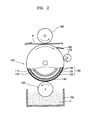
- FIG. 2 is a schematic view of an image forming apparatus according to an embodiment of the present invention.
- FIG. 3 is a perspective view of a rotating drum 100 as an electrostatic latent image forming medium illustrated in FIG. 2.
- the image forming apparatus includes the electrostatic latent image forming medium, a toner supplying unit, and a transferring unit.
- the image forming apparatus may further include a charging unit depending on how an electrostatic latent image is formed.
- the electrostatic latent image forming medium forms an electrostatic latent image that corresponds to an image to be printed thereon.
- a rotating drum 100 may be used as the electrostatic latent image forming medium.
- the rotating drum 100 includes a thin film transistor (TFT) array 120 and a capacitor layer 130 stacked sequentially on a surface of a cylindrical frame 110.
- the TFT array 120 is stacked on the surface of the frame 110 and includes a plurality of TFTs 122a and 122b presented in FIG. 4.
- the capacitor layer 130 includes a common electrode 132 formed on the TFT array 120, a dielectric layer 134 formed on the common electrode 132, and a plurality of pixel electrodes 136 arranged on a surface of the dielectric layer 134.
- the number of the pixel electrodes 136 depends on the degree of resolution required by the image forming apparatus. In other words, the number of the pixel electrodes 136 is the same as the number of pixels of an image.
- An array of the pixel electrodes 136 is formed on the surface of the dielectric layer 134 as illustrated in FIG. 3.
- a protective layer 140 protecting the dielectric layer 134 and the pixel electrodes 136 may be formed on a surface of the capacitor layer 130, i.e., surfaces of the dielectric layer 134 and the pixel electrodes 136.
- the rotating drum 100 is used as an electrostatic latent image forming medium
- a belt circulating along a predetermined path may also be used as the electrostatic latent image forming medium.
- the toner supplying unit supplies toner T to an electrostatic latent image formed on a surface of the rotating drum 100 and develops the electrostatic latent image into a toner image.
- a variety of devices known to those skilled in the art may be used as the toner supplying unit.
- a toner supplying roller 150 rotating in contact with the toner T stored in a toner container 152 may be used as illustrated in FIG. 2.
- the toner supplying roller 150 adheres the toner T stored in the toner container 152 to the surface of the rotating drum 100 while rotating in synchronization with the rotating drum 100.
- the toner T adhered to a surface of the toner supplying roller 150 is moved and adhered to an electrostatic latent image on the rotating drum 100 by a difference between a potential of the surface of the toner supplying roller 150 and a potential of the electrostatic latent image.
- the transferring unit transfers the developed toner image on the surface of the rotating drum 100 to a printing medium, for example, a sheet of paper P.
- a transferring roller 160 may be used as the transferring unit.
- the transferring roller 160 is disposed parallel to the rotating drum 100 such that it can rotate simultaneously with the rotating drum 100.
- the sheet of paper P passes between the transferring roller 160 and the rotating drum 100. In this process, the developed toner image on the surface of the rotating drum 100 is transferred to the sheet of paper P.
- the transferring unit may include an intermediate transferring belt (not shown).
- the developed toner image on the surface of the rotating drum 100 is initially transferred to the intermediate transferring belt. Then, the developed toner image is transferred to the sheet of paper from the intermediate transferring belt by the transferring roller 160.
- Most of the image forming apparatuses for printing color images include intermediate transferring belts as transferring units. If an intermediate transferring belt is included in an image forming apparatus, a plurality of rotating drums 100 are arranged in series along a path of the intermediate transferring belt.
- the charging unit charges the surface of the rotating drum 100 with a predetermined potential.
- a charging roller 170 supplying electric charges to the surface of the rotating drum 100 while rotating in contact with the surface of the rotating drum 100 may be used as the charging unit.
- a corona wire may be used as the charging unit.
- a cleaning unit removing the toner T remaining on the surface of the rotating drum 100 after the toner image is transferred to the sheet of paper P may be placed near the rotating drum 100.
- a cleaning blade 180 contacting the surface of the rotating drum 100 may be used as the cleaning unit.
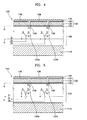
- FIGS. 4 and 5 are sectional views of the rotating drum 100 illustrated in FIG. 2 according to an embodiment of the present invention.
- FIG. 4 is a sectional view of the rotating drum 100 before an electrostatic latent image is formed thereon.
- FIG. 5 is a sectional view of the rotating drum 100 after an electrostatic latent image is formed thereon.
- the rotating drum 100 includes the frame 110, the TFT array 120, and the capacitor layer 130 stacked sequentially as described above.
- the TFT array 120 is stacked on the surface of the frame 110 and includes the TFTs 122a and 122b arranged uniformly.
- the sources S of the TFTs 122a and 122b are grounded via a source electrode line S 1 , and the gates G of the same are connected to gate electrode lines G1 and G2, respectively, such that voltages can be selectively applied to the gates G.
- the drains D of the TFTs 122a and 122b are connected to the pixel electrodes 136 via drain electrode lines D 1 and D 2 , respectively.
- the capacitor layer 130 is formed on the TFT array 120 and includes the common electrode 132, the dielectric layer 134, and the pixel electrodes 136 stacked sequentially.
- the common electrode 132 is grounded and may be formed as a layer covering the entire bottom surface of the dielectric layer 134.
- a plurality of holes 138 are formed in the common electrode 132 to insulate the common electrode 132 from the drain electrode lines D 1 and D 2 .
- the pixel electrodes 136 corresponding to pixels, respectively, are formed on the dielectric layer 134 and electrically connected to the drains D of the TFTs 122a and 122b via the drain electrode lines D 1 and D 2 , respectively.
- the protective layer 140 protecting the dielectric layer 134 and the pixel electrodes 136 may be formed on the capacitor layer 130 and may be formed of an abrasion resistant material.
- FIG. 4 illustrates the rotating drum 100, the surface of which is charged with a negative potential.
- the surface of the rotating drum 100 may be charged with a positive potential.
- the surface potential of the rotating drum 100 depends on polarity of the potential of the toner T used in an image forming apparatus. In other words, if toner T charged with a negative potential is used, the surface of the rotating drum 100 is charged with negative potential. Conversely, if toner T charged with a positive potential is used, the surface of the rotating drum 100 is charged with the positive potential.
- voltages are selectively applied to the gates G of the TFTs 122a and 122b.
- the source S and the drain D of the TFT 122a are electrically connected. Accordingly, electric charges on the surface of the pixel electrode 136 connected to the drain D of the TFT 122a drain out via the drain electrode line D 1 and the grounded source electrode line S 1 .
- the surface potential of the rotating drum 100 can be controlled per each pixel electrode 136. Therefore, an electrostatic latent image with a potential different from a potential of its surrounding area is formed on the surface of the rotating drum 100. A potential difference between the electrostatic latent image and the toner supplying roller 150 and a potential difference between the surrounding area of the electrostatic latent image and the toner supplying roller 150 are different. Therefore, the toner T with a predetermined potential is adhered only to the electrostatic latent image, thereby forming a toner image.
- an electrostatic latent image can be formed on the surface of the rotating drum 100 using the TFT array 120.
- the configuration of the image forming apparatus is simplified, resulting in a reduction in its size and manufacturing cost.
- an entire electrostatic latent image can be formed electrically simultaneously. Therefore, the image forming apparatus according to the present invention can perform printing at a fast speed since the time spent on scanning a laser beam, which was previously performed per line, can be reduced.
- the present invention can achieve high resolution since the pixel electrodes 136 can be formed in a very small size using a micro manufacturing process used in a semiconductor fabrication process.
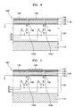
- FIGS. 6 and 7 are sectional views of a rotating drum 100' illustrated in FIG. 2 according to another embodiment of the present invention.
- FIG. 6 is a sectional view of the rotating drum 100' before an electrostatic latent image is formed thereon.
- FIG. 7 is a sectional view of the rotating drum 100' after an electrostatic latent image is formed thereon. Since the sectional structure of the rotating drum 100' of FIGS. 6 and 7 are identical to that of the rotating drum 100 of FIG. 4 except for wirings of TFTs 124a and 124b, a detailed description will be focused on the difference between them.
- the rotating drum 100' includes a TFT array 120' stacked on a surface of a frame 110 and the TFTs 124a and 124b arranged uniformly in the TFT array 120'.
- Voltages are applied to the gates G of the TFTs 124a and 124b via a common gate electrode line G 1 .
- the sources S of the TFTs 124a and 124b are connected to source electrode lines S 1 and S 2 , respectively, such that voltages can be selectively applied to the sources S.
- the drains D of the TFTs 124a and 124b are connected to a plurality of pixel electrodes 136 via drain electrode lines D 1 and D 2 , respectively.
- a capacitor layer 130 is stacked on the TFT array 120'.
- the pixel electrodes 136 formed on the capacitor layer 130 are electrically connected to the drains D of the TFTs 124a and 124b via the drain electrode lines D 1 and D 2 , respectively.
- voltages are selectively applied to the gates G and sources S of the TFTs 124a and 124b. If a voltage is applied to the gate G and the source S of the TFT 124a, electric charges are injected into the pixel electrode 136 connected to the drain D of the TFT 124a via the drain D. The electric charges thus injected are stored in a portion of the capacitor layer 130 corresponding to the pixel electrode 136. Accordingly, the portion storing the electric charges and portions without electric charges coexist on the surface of the rotating drum 100', and these portions have different potentials.
- the surface potential of the rotating drum 100' can be controlled per pixel electrode 136. Therefore, an electrostatic latent image corresponding to an image to be printed can be formed.
- a potential difference between the electrostatic latent image thus formed and the toner supplying roller 150 and a potential difference between the surrounding area of the electrostatic latent image and the toner supplying roller 150 are different. Therefore, the toner T with a predetermined potential is adhered only to the electrostatic latent image, thereby forming a toner image.
- the rotating drum 100' in such a structure illustrated in FIGS. 6 and 7 may achieve the effects described above.
- an image forming apparatus forms an electrostatic latent image on a surface of an electrostatic latent image forming medium by using a TFT array included in the electrostatic latent image forming medium.
- the image forming apparatus has a simpler configuration than a conventional image forming apparatus including a complicated LSU, resulting in a reduction in size and manufacturing cost.
- an entire electrostatic latent image can be formed electrically. Therefore, a fast printing speed can be achieved since the time spent on scanning a laser beam can be reduced.
- the image forming apparatus can achieve high resolution by forming a plurality of pixel electrodes in a very small size using a micro manufacturing process.
Landscapes
- Physics & Mathematics (AREA)
- General Physics & Mathematics (AREA)
- Health & Medical Sciences (AREA)
- Engineering & Computer Science (AREA)
- Biomedical Technology (AREA)
- Heart & Thoracic Surgery (AREA)
- Vascular Medicine (AREA)
- Life Sciences & Earth Sciences (AREA)
- Animal Behavior & Ethology (AREA)
- General Health & Medical Sciences (AREA)
- Public Health (AREA)
- Veterinary Medicine (AREA)
- Printers Or Recording Devices Using Electromagnetic And Radiation Means (AREA)
- Photoreceptors In Electrophotography (AREA)
- Electrophotography Using Other Than Carlson'S Method (AREA)
Applications Claiming Priority (2)
| Application Number | Priority Date | Filing Date | Title |
|---|---|---|---|
| KR2004035548 | 2004-05-19 | ||
| KR1020040035548A KR100634504B1 (ko) | 2004-05-19 | 2004-05-19 | 박막 트랜지스터 어레이를 이용한 정전잠상 형성매체와이를 구비한 화상형성장치 |
Publications (2)
| Publication Number | Publication Date |
|---|---|
| EP1598709A2 true EP1598709A2 (de) | 2005-11-23 |
| EP1598709A3 EP1598709A3 (de) | 2007-03-28 |
Family
ID=34941301
Family Applications (1)
| Application Number | Title | Priority Date | Filing Date |
|---|---|---|---|
| EP05252962A Withdrawn EP1598709A3 (de) | 2004-05-19 | 2005-05-13 | Medium zur Erzeugung latenter Elektrostatischer Bilder mittels einer TFT matrix und Bilderzeugungsvorrichtung mit diesem Medium |
Country Status (4)
| Country | Link |
|---|---|
| US (1) | US7388594B2 (de) |
| EP (1) | EP1598709A3 (de) |
| JP (1) | JP2005331955A (de) |
| KR (1) | KR100634504B1 (de) |
Cited By (1)
| Publication number | Priority date | Publication date | Assignee | Title |
|---|---|---|---|---|
| WO2008055115A1 (en) * | 2006-10-30 | 2008-05-08 | Hewlett-Packard Development Company, L.P. | Methods and devices for electrophotographic printing |
Families Citing this family (12)
| Publication number | Priority date | Publication date | Assignee | Title |
|---|---|---|---|---|
| KR20080101518A (ko) * | 2007-05-18 | 2008-11-21 | 삼성전자주식회사 | 화상형성장치 및 방법 |
| KR20080112009A (ko) * | 2007-06-20 | 2008-12-24 | 삼성전자주식회사 | 화상형성장치 및 방법 |
| US7995081B2 (en) * | 2008-06-25 | 2011-08-09 | Palo Alto Research Center Incorporated | Anisotropically conductive backside addressable imaging belt for use with contact electrography |
| JP5206401B2 (ja) * | 2008-12-25 | 2013-06-12 | 富士ゼロックス株式会社 | 画像形成装置 |
| US8643685B2 (en) * | 2009-02-06 | 2014-02-04 | Xerox Corporation | Photoreceptor with a TFT backplane for xerography without a ROS system |
| US8854403B2 (en) * | 2009-02-06 | 2014-10-07 | Xerox Corporation | Image forming apparatus with a TFT backplane for xerography without a light source |
| JP5402653B2 (ja) | 2010-01-13 | 2014-01-29 | 富士ゼロックス株式会社 | 像保持体及びこれを用いた画像形成装置 |
| JP5569277B2 (ja) * | 2010-09-09 | 2014-08-13 | 富士ゼロックス株式会社 | 像保持体及びこれを用いた画像形成装置 |
| US8587622B2 (en) * | 2011-02-25 | 2013-11-19 | Xerox Corporation | Generation of digital electrostatic latent images and data communications system using rotary contacts |
| EP2839346A1 (de) * | 2012-04-19 | 2015-02-25 | OCE-Technologies B.V. | Bilderzeugungsvorrichtung mit einem direkten bilderzeugungselement |
| US11520248B2 (en) | 2018-12-12 | 2022-12-06 | Hewlett-Packard Development Company, L.P. | Transferring printing fluid to a substrate |
| CN113721432B (zh) * | 2021-09-16 | 2025-02-11 | 北京京东方技术开发有限公司 | 电控鼓及其制作方法、打印机 |
Family Cites Families (8)
| Publication number | Priority date | Publication date | Assignee | Title |
|---|---|---|---|---|
| JPS57124367A (en) * | 1981-01-26 | 1982-08-03 | Canon Inc | Image forming method and its device |
| JPS61130058A (ja) * | 1984-11-30 | 1986-06-17 | Mita Ind Co Ltd | 静電式画像形成装置 |
| JPS62127853A (ja) * | 1985-11-29 | 1987-06-10 | Mita Ind Co Ltd | 画像形成方法 |
| JP3233463B2 (ja) * | 1992-09-25 | 2001-11-26 | 株式会社東芝 | 像形成体、この像形成体を含む像担持体及びこの像形成体を組み込んだ画像形成装置並びに画像形成方法 |
| US6100909A (en) * | 1998-03-02 | 2000-08-08 | Xerox Corporation | Matrix addressable array for digital xerography |
| JP4138106B2 (ja) * | 1998-10-22 | 2008-08-20 | セイコーエプソン株式会社 | 電子ペーパー用プリンター |
| JP3826013B2 (ja) * | 2001-02-28 | 2006-09-27 | キヤノン株式会社 | 画像形成装置 |
| JP4443798B2 (ja) * | 2001-07-18 | 2010-03-31 | 株式会社リコー | デジタル画像形成素子及び画像形成方法 |
-
2004
- 2004-05-19 KR KR1020040035548A patent/KR100634504B1/ko not_active Expired - Fee Related
-
2005
- 2005-05-13 EP EP05252962A patent/EP1598709A3/de not_active Withdrawn
- 2005-05-18 US US11/131,238 patent/US7388594B2/en not_active Expired - Fee Related
- 2005-05-18 JP JP2005145686A patent/JP2005331955A/ja active Pending
Cited By (2)
| Publication number | Priority date | Publication date | Assignee | Title |
|---|---|---|---|---|
| WO2008055115A1 (en) * | 2006-10-30 | 2008-05-08 | Hewlett-Packard Development Company, L.P. | Methods and devices for electrophotographic printing |
| US8749600B2 (en) | 2006-10-30 | 2014-06-10 | Hewlett-Packard Development Company, L.P. | Methods and devices for electrophotographic printing |
Also Published As
| Publication number | Publication date |
|---|---|
| JP2005331955A (ja) | 2005-12-02 |
| EP1598709A3 (de) | 2007-03-28 |
| KR100634504B1 (ko) | 2006-10-16 |
| US7388594B2 (en) | 2008-06-17 |
| US20050259140A1 (en) | 2005-11-24 |
| KR20050110738A (ko) | 2005-11-23 |
Similar Documents
| Publication | Publication Date | Title |
|---|---|---|
| EP0508355B1 (de) | Vorrichtung zum Aufladen eines lichtempfindlichen Körpers | |
| US6970666B2 (en) | Image forming apparatus | |
| US7388594B2 (en) | Electrostatic latent image forming medium, image forming apparatus including the electrostatic latent image forming medium and method of forming an electrostatic latent image | |
| JP2000162881A (ja) | 転写装置、画像形成装置、転写方法、及び、画像形成方法 | |
| US20110158666A1 (en) | Image forming device that executes reverse-transfer operation | |
| US7796912B2 (en) | Image forming method and apparatus which uses alternating voltage to form an electric field for moving toner | |
| JP3766254B2 (ja) | 電子写真装置 | |
| US7782355B2 (en) | Image forming apparatus using a plurality of lasers with a varying exposure ratio | |
| US7317884B2 (en) | Image forming apparatus featuring a defined relationship among an image length, transforming member length, and length of an electric field area | |
| JP3998339B2 (ja) | 電子写真装置 | |
| US7676181B2 (en) | Developing unit and image forming device | |
| JPH06314035A (ja) | 画像形成装置 | |
| US5812904A (en) | Image forming apparatus and method for controlling charging potential differently between image forming area and non-image forming area of photosensitive drum | |
| KR100423459B1 (ko) | 칼라 화상형성장치 | |
| US7417653B2 (en) | Electrostatic latent image forming medium using optical shutter array and image forming apparatus having the same | |
| JP3826565B2 (ja) | 画像形成装置 | |
| JP2003066797A (ja) | 画像形成装置およびプロセスカートリッジ | |
| JP2912258B2 (ja) | 背面露光記録画像形成装置 | |
| JPH1039550A (ja) | 両面画像形成装置 | |
| CN100527013C (zh) | 图像转印单元、电子照相成像装置以及电子照相成像方法 | |
| JP2003159836A (ja) | 画像形成装置 | |
| JP2006098508A (ja) | 画像形成装置 | |
| JP2004106365A (ja) | 画像形成装置および複写装置 | |
| JPH09311602A (ja) | 画像形成装置 | |
| JPH09311509A (ja) | 画像形成装置 |
Legal Events
| Date | Code | Title | Description |
|---|---|---|---|
| PUAI | Public reference made under article 153(3) epc to a published international application that has entered the european phase |
Free format text: ORIGINAL CODE: 0009012 |
|
| AK | Designated contracting states |
Kind code of ref document: A2 Designated state(s): AT BE BG CH CY CZ DE DK EE ES FI FR GB GR HU IE IS IT LI LT LU MC NL PL PT RO SE SI SK TR |
|
| AX | Request for extension of the european patent |
Extension state: AL BA HR LV MK YU |
|
| PUAL | Search report despatched |
Free format text: ORIGINAL CODE: 0009013 |
|
| AK | Designated contracting states |
Kind code of ref document: A3 Designated state(s): AT BE BG CH CY CZ DE DK EE ES FI FR GB GR HU IE IS IT LI LT LU MC NL PL PT RO SE SI SK TR |
|
| AX | Request for extension of the european patent |
Extension state: AL BA HR LV MK YU |
|
| RIC1 | Information provided on ipc code assigned before grant |
Ipc: G03G 15/00 20060101ALI20070221BHEP Ipc: G03G 15/32 20060101AFI20050830BHEP |
|
| 17P | Request for examination filed |
Effective date: 20070815 |
|
| 17Q | First examination report despatched |
Effective date: 20070920 |
|
| AKX | Designation fees paid |
Designated state(s): DE FR GB |
|
| RAP1 | Party data changed (applicant data changed or rights of an application transferred) |
Owner name: SAMSUNG ELECTRO-MECHANICS CO., LTD. |
|
| GRAP | Despatch of communication of intention to grant a patent |
Free format text: ORIGINAL CODE: EPIDOSNIGR1 |
|
| INTG | Intention to grant announced |
Effective date: 20140226 |
|
| RIN1 | Information on inventor provided before grant (corrected) |
Inventor name: KWON, JANG-YEON, D-3403 MICHELAN CHEREVILLE Inventor name: KWON, KYE-SI, 503-410 BANPO MIDO 2-CHA APT. Inventor name: KIM, SEONG-JIN, 120-904 PARK TOWN SAMICK APT. Inventor name: SHIN, SEUNG-JOO, 1116-1506 JUGONG APT. Inventor name: MOON, IL-KWON, 113-2004 NEULPUREUN BYUCKSAN APT. |
|
| STAA | Information on the status of an ep patent application or granted ep patent |
Free format text: STATUS: THE APPLICATION IS DEEMED TO BE WITHDRAWN |
|
| 18D | Application deemed to be withdrawn |
Effective date: 20140709 |