EP1594349A1 - Elektronisches Vorschaltgerät für eine Lampe - Google Patents
Elektronisches Vorschaltgerät für eine Lampe Download PDFInfo
- Publication number
- EP1594349A1 EP1594349A1 EP05008806A EP05008806A EP1594349A1 EP 1594349 A1 EP1594349 A1 EP 1594349A1 EP 05008806 A EP05008806 A EP 05008806A EP 05008806 A EP05008806 A EP 05008806A EP 1594349 A1 EP1594349 A1 EP 1594349A1
- Authority
- EP
- European Patent Office
- Prior art keywords
- damping element
- electronic ballast
- capacitor
- commutation
- switching device
- Prior art date
- Legal status (The legal status is an assumption and is not a legal conclusion. Google has not performed a legal analysis and makes no representation as to the accuracy of the status listed.)
- Granted
Links
- 239000003990 capacitor Substances 0.000 claims abstract description 38
- 238000013016 damping Methods 0.000 claims description 32
- XEEYBQQBJWHFJM-UHFFFAOYSA-N Iron Chemical compound [Fe] XEEYBQQBJWHFJM-UHFFFAOYSA-N 0.000 claims description 6
- 229910000859 α-Fe Inorganic materials 0.000 claims description 4
- 239000004020 conductor Substances 0.000 claims description 3
- 229910052742 iron Inorganic materials 0.000 claims description 3
- 239000004065 semiconductor Substances 0.000 claims description 2
- 230000001939 inductive effect Effects 0.000 abstract 1
- 238000011084 recovery Methods 0.000 abstract 1
- 230000000712 assembly Effects 0.000 description 1
- 238000000429 assembly Methods 0.000 description 1
- 230000002238 attenuated effect Effects 0.000 description 1
- 230000001419 dependent effect Effects 0.000 description 1
- 230000005669 field effect Effects 0.000 description 1
- 230000010355 oscillation Effects 0.000 description 1
Images


Classifications
-
- H—ELECTRICITY
- H05—ELECTRIC TECHNIQUES NOT OTHERWISE PROVIDED FOR
- H05B—ELECTRIC HEATING; ELECTRIC LIGHT SOURCES NOT OTHERWISE PROVIDED FOR; CIRCUIT ARRANGEMENTS FOR ELECTRIC LIGHT SOURCES, IN GENERAL
- H05B41/00—Circuit arrangements or apparatus for igniting or operating discharge lamps
- H05B41/14—Circuit arrangements
- H05B41/26—Circuit arrangements in which the lamp is fed by power derived from DC by means of a converter, e.g. by high-voltage DC
- H05B41/28—Circuit arrangements in which the lamp is fed by power derived from DC by means of a converter, e.g. by high-voltage DC using static converters
Definitions
- the present invention relates to an electronic ballast for a lamp with an input circuit with a connection to a power supply, an output circuit with one connection for the lamp and one between the input and the output circuit arranged voltage converter device, wherein the voltage converter device an input capacitor and an output capacitor between which a switching device and a freewheeling diode, and at least one damping element, at least one trapezoidal capacitor and an inductance are arranged, wherein the Voltage converter device is designed to perform a commutation, wherein the current flow before and after the commutation is defined in each case a main circuit.
- FIG. 1 schematically illustrated, wherein the input circuit, the reference numeral 10, the voltage converter device the reference numeral 12 and the output circuit carries the reference numeral 14.
- the lamp is with the Reference numeral 16 marked.
- FIG. 2 A more detailed illustration of the prior art FIG. 2 is taken from the circuit arrangement used as voltage converter device 12 become. This has on the input side an input capacitor C1 and the output side an output capacitor C2.
- the circuit shown here by way of example is formed as a buck converter and has a switching device T1, in this case a transistor, a freewheeling diode D1, a trapezoidal capacitor C3 and an inductance L1.
- the switching device T 1 and the inductance L1 are arranged in the longitudinal branch, the freewheeling diode D1 and the trapezoidal capacitor C3 are each arranged in a shunt branch.
- a trapezoidal capacitor is used to adjust the switching speed of the switching device.
- the inductance L1 is dimensioned in the usual way as a storage throttle and ensures that a current flow is maintained after the commutation.
- a damping element serially to the switching device T1 L2, preferably a ferrite, arranged.
- the damping element also be designed as sheet iron or as at least one conductor loop.
- the present invention is therefore based on the object, a generic electronic Further develop ballast in such a way that allows automatic assembly is and a significant reduction of the space occupied by the damping element can be achieved.
- an electronic ballast having the features of The invention is based on the finding that the damping element can be made significantly smaller when it no longer flows through the main stream becomes. Characterized in that the damping element in a clever manner in a secondary circuit is arranged, it is no longer traversed by the load current, so that the DC resistance only plays a minor role. Nevertheless, it may be that of cause him desired attenuation of high-frequency vibrations. At the same damping Therefore, a significantly smaller component can be selected as in the known Realization. If the size is maintained, can with the inventive invention electronic ballast significantly better damping properties can be achieved than in the prior art.
- the voltage converter device is designed so that before commutation the switching device and after commutation the freewheeling diode of Current flows through, or vice versa, and between these two phases the at least a series circuit of damping element and trapezoidal capacitor flows through current becomes.
- exactly one series circuit of damping element and trapezoidal capacitor present, parallel to the switching device or parallel to the freewheeling diode is arranged.
- two series circuits can each consist of one Damping element and a trapezoidal capacitor be present, with a first such Series connection in parallel with the switching device and a second such series connection is arranged parallel to the freewheeling diode.
- the damping element depending on the frequency range in which the Voltage converter device operates as ferrite, as iron sheet or as at least one Be conductor loop formed.
- the at least one damping element is as SMD component performed, allowing easy automatic assembly becomes.
- FIG. 3 shows three different embodiments of a voltage converter device, as used in an electronic ballast according to the invention.
- the three embodiments shown in FIG. 3 each serve to realize a Step-down converter.
- Commutation defined a first main circuit, the dashed lines shown here and the components input capacitor C1, switching device T1, inductance L1 and Output capacitor C2 comprises.
- the current flows in the dash-dotted circle, comprising the freewheeling diode D1, the inductance L1 and the output capacitor C2.
- the current flows through the series circuit of trapezoidal capacitor C3 and damping element L2 and output capacitor C2.
- the Current flow before and after commutation which defines a main circuit is, is the series circuit of trapezoidal capacitor C3 and attenuator L2 in one Subcircuit arranged.
- the respective main circuit comprises before the commutation and the respective main circuit after the commutation the same elements as already in connection with the embodiment of Fig. 3a executed.
- the figures according to the embodiments 3b and 3c only the current flow during the commutation dotted registered. While in the embodiment according to the figure 3b, the series circuit of damping element L2 and trapezoidal capacitor C3 is arranged in a bypass circuit which is parallel is arranged to the switching device T1, are in the embodiment according to Fig. 3c in Comparison with the embodiment according to FIG.
- two series circuits of damping element and trapezoidal capacitor present namely a first series circuit, the Damping element L2a and the trapezoidal capacitor C3a comprises, and a second series circuit, comprising the attenuator L2b and the trapezoidal capacitor C3b.
- the first series connection is arranged parallel to the switching device T1
- the second Series connection is arranged parallel to the free-wheeling diode D1.
- main circuits are both series circuits each in a secondary circuit.
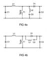
- FIGS. 4 a and 4b an electronic ballast according to the invention realize each one Up converter.
- the main circuit before Commutation the elements input capacitor C1, inductor L1 and switching device T1 the main circuit after commutation the elements input capacitor C1, inductor L1, freewheeling diode D1 and output capacitor C2.
- the current flows during the commutation phase through the components input capacitor C1, inductance L1, damping element L2, trapezoidal capacitor C3 and output capacitor C2.
- a voltage converter device may be incorporated
Landscapes
- Circuit Arrangements For Discharge Lamps (AREA)
- Dc-Dc Converters (AREA)
- Inverter Devices (AREA)
Abstract
Description
- Fig. 1
- in schematischer Darstellung die Baugruppen eines aus dem Stand der Technik bekannten elektronischen Vorschaltgeräts;
- Fig. 2
- eine aus dem Stand der Technik bekannte Spannungskonvertervorrichtung wie sie beispielhaft in der im elektronischen Vorschaltgerät von Fig. 1 eingesetzt wird;
- Fig. 3
- drei unterschiedliche Ausführungsformen der Spannungskonvertervorrichtung bei einem erfindungsgemäßen elektronischen Vorschaltgerät, wobei die jeweilige Spannungskonvertervorrichtung als Tiefsetzsteller ausgeführt ist;
- Fig. 4
- zwei unterschiedliche Ausführungsformen der Spannungskonvertervorrichtung bei einem erfindungsgemäßen elektronischen Vorschaltgerät, wobei die jeweilige Spannungskonvertervorrichtung als Hochsetzsteller ausgeführt ist.
Claims (8)
- Elektronisches Vorschaltgerät für eine Lampe (16) mitdadurch gekennzeichnet, dass mindestens ein Dämpfungselement (L2) und mindestens ein Trapezkondensator (C3) in Serie geschaltet sind und eine derartige Serienschaltung in einem Nebenstromkreis angeordnet ist.einem Eingangskreis (10) mit einem Anschluss an eine Spannungsversorgung,einem Ausgangskreis (14) mit einem Anschluss für die Lampe (16), undeiner zwischen dem Eingangs- und dem Ausgangskreis (10, 14) angeordneten Spannungskonvertervorrichtung (12), wobei die Spannungskonvertervorrichtung einen Eingangskondensator (C1) und einen Ausgangskondensator (C2) umfasst, zwischen denen eine Schaltvorrichtung (T1) und eine Freilaufdiode (D1), sowie mindestens ein Dämpfungselement (L2), mindestens ein Trapezkondensator (C3) und eine Induktivität (L1) angeordnet sind, wobei die Spannungskonvertervorrichtung (12) ausgelegt ist, eine Kommutierung auszuführen, wobei durch den Stromfluss vor und nach der Kommutierung jeweils ein Hauptstromkreis definiert ist,
- Elektronisches Vorschaltgerät nach Anspruch 1,
dadurch gekennzeichnet, dass die Schaltvorrichtung (T1) und die Freilaufdiode (D1) als zwei separate Halbleiterbauelemente ausgeführt sind. - Elektronisches Vorschaltgerät nach einem der Ansprüche 1 oder 2,
dadurch gekennzeichnet, dass die Spannungskonvertervorrichtung (12) so ausgelegt ist, dass vor der Kommutierung die Schaltvorrichtung (T1) und nach der Kommutierung die Freilaufdiode (D1) von Strom durchflossen wird, oder umgekehrt, und zwischen diesen beiden Phasen die mindestens eine Serienschaltung aus Dämpfungselement (L2) und Trapezkondensator (C3) von Strom durchflossen wird. - Elektronisches Vorschaltgerät nach einem der vorhergehenden Ansprüche,
dadurch gekennzeichnet, dass mindestens eine Serienschaltung aus Dämpfungselement (L2) und Trapezkondensator (C3) vorhanden ist, wobei diese parallel zur Schaltvorrichtung (T1) und/oder parallel zur Freilaufdiode (D1) angeordnet ist. - Elektronisches Vorschaltgerät nach Anspruch 4,
dadurch gekennzeichnet, dass genau eine Serienschaltung aus Dämpfungselement (L2) und Trapezkondensator (C3) vorhanden ist, die parallel zur Schaltvorrichtung oder parallel zur Freilaufdiode (D1) angeordnet ist. - Elektronisches Vorschaltgerät nach Anspruch 4,
dadurch gekennzeichnet, dass zwei Serienschaltungen aus jeweils einem Dämpfungselement (L2a, L2b) und einem Trapazkondensator (C3a, C3b) vorhanden sind, wobei eine erste derartige Serienschaltung parallel zur Schaltvorrichtung (T1) und eine zweite derartige Serienschaltung parallel zur Freilaufdiode (D1) angeordnet ist. - Elektronisches Vorschaltgerät nach einem der vorhergehenden Ansprüche,
dadurch gekennzeichnet, dass das Dämpfungselement (L2, L2a, L2b) als Ferrit, als Eisenblech oder als mindestens eine Leiterschleife ausgebildet ist. - Elektronisches Vorschaltgerät nach einem der vorhergehenden Ansprüche,
dadurch gekennzeichnet, dass der mindestens eine Dämpfungselement (L2, L2a, L2b) als SMD-Bauelement ausgeführt ist.
Applications Claiming Priority (2)
| Application Number | Priority Date | Filing Date | Title |
|---|---|---|---|
| DE102004022571 | 2004-05-07 | ||
| DE102004022571A DE102004022571A1 (de) | 2004-05-07 | 2004-05-07 | Elektronisches Vorschaltgerät für eine Lampe |
Publications (2)
| Publication Number | Publication Date |
|---|---|
| EP1594349A1 true EP1594349A1 (de) | 2005-11-09 |
| EP1594349B1 EP1594349B1 (de) | 2007-02-21 |
Family
ID=34935568
Family Applications (1)
| Application Number | Title | Priority Date | Filing Date |
|---|---|---|---|
| EP05008806A Expired - Lifetime EP1594349B1 (de) | 2004-05-07 | 2005-04-21 | Elektronisches Vorschaltgerät für eine Lampe |
Country Status (7)
| Country | Link |
|---|---|
| US (1) | US7193372B2 (de) |
| EP (1) | EP1594349B1 (de) |
| JP (1) | JP4833584B2 (de) |
| AT (1) | ATE354933T1 (de) |
| CA (1) | CA2506368A1 (de) |
| DE (2) | DE102004022571A1 (de) |
| TW (1) | TWI422283B (de) |
Cited By (2)
| Publication number | Priority date | Publication date | Assignee | Title |
|---|---|---|---|---|
| DE102008044372A1 (de) | 2008-12-05 | 2010-06-10 | Robert Bosch Gmbh | Schaltungsanordnung für eine Leuchtvorrichtung, Leuchtvorrichtung und Verfahren |
| DE102016223153A1 (de) | 2016-11-23 | 2018-05-24 | Osram Gmbh | Betreiben eines vorschaltgeräts für eine gasentladungslampe |
Families Citing this family (3)
| Publication number | Priority date | Publication date | Assignee | Title |
|---|---|---|---|---|
| DE102005056255A1 (de) * | 2005-11-25 | 2007-06-06 | Patent-Treuhand-Gesellschaft für elektrische Glühlampen mbH | Schaltungsvorrichtung mit obenliegendem Buck-Transistor |
| KR100823194B1 (ko) * | 2006-11-20 | 2008-04-18 | 삼성에스디아이 주식회사 | 플라즈마 표시 장치 및 그 구동 장치 |
| US7579814B2 (en) * | 2007-01-12 | 2009-08-25 | Potentia Semiconductor Corporation | Power converter with snubber |
Citations (1)
| Publication number | Priority date | Publication date | Assignee | Title |
|---|---|---|---|---|
| US5932974A (en) * | 1996-06-04 | 1999-08-03 | International Rectifier Corporation | Ballast circuit with lamp removal protection and soft starting |
Family Cites Families (12)
| Publication number | Priority date | Publication date | Assignee | Title |
|---|---|---|---|---|
| JPH06101930B2 (ja) * | 1988-09-16 | 1994-12-12 | 九州大学長 | スイッチング電源装置 |
| JPH05328714A (ja) * | 1991-04-24 | 1993-12-10 | Shindengen Electric Mfg Co Ltd | Dc−dcコンバータ |
| JP3261142B2 (ja) * | 1991-05-15 | 2002-02-25 | 松下電工株式会社 | 放電灯点灯装置 |
| JPH07274500A (ja) * | 1994-03-24 | 1995-10-20 | Sony Corp | 電源回路 |
| US5528111A (en) * | 1994-12-02 | 1996-06-18 | Motorola, Inc. | Ballast circuit for powering gas discharge lamp |
| JP3036694U (ja) * | 1995-03-20 | 1997-05-02 | スーパー・3−ディー・オプティカル・エクィプメンツ・カンパニー・リミテッド | 立体写真露光装置 |
| JP2859611B2 (ja) * | 1998-04-17 | 1999-02-17 | 株式会社東芝 | スイッチングレギュレータ |
| US5969484A (en) * | 1998-05-14 | 1999-10-19 | Optimum Power Conversion, Inc. | Electronic ballast |
| JP3374916B2 (ja) * | 2000-10-02 | 2003-02-10 | サンケン電気株式会社 | Dc−dcコンバータ |
| US6465991B1 (en) * | 2001-07-30 | 2002-10-15 | Koninklijke Philips Electronics N.V. | Switchable power converter with coupled inductor boost and coupled inductor SEPIC for multiple level input line power factor correction |
| CN100469210C (zh) * | 2001-10-31 | 2009-03-11 | 皇家飞利浦电子股份有限公司 | 镇流电路 |
| DE10200046A1 (de) * | 2002-01-02 | 2003-07-17 | Patent Treuhand Ges Fuer Elektrische Gluehlampen Mbh | Betriebsgerät für Hochdruck-Entladungslampen |
-
2004
- 2004-05-07 DE DE102004022571A patent/DE102004022571A1/de not_active Withdrawn
-
2005
- 2005-04-21 EP EP05008806A patent/EP1594349B1/de not_active Expired - Lifetime
- 2005-04-21 AT AT05008806T patent/ATE354933T1/de not_active IP Right Cessation
- 2005-04-21 DE DE502005000388T patent/DE502005000388D1/de not_active Expired - Lifetime
- 2005-05-03 TW TW094114233A patent/TWI422283B/zh not_active IP Right Cessation
- 2005-05-04 CA CA002506368A patent/CA2506368A1/en not_active Abandoned
- 2005-05-04 US US11/121,066 patent/US7193372B2/en not_active Expired - Fee Related
- 2005-05-06 JP JP2005135335A patent/JP4833584B2/ja not_active Expired - Fee Related
Patent Citations (1)
| Publication number | Priority date | Publication date | Assignee | Title |
|---|---|---|---|---|
| US5932974A (en) * | 1996-06-04 | 1999-08-03 | International Rectifier Corporation | Ballast circuit with lamp removal protection and soft starting |
Non-Patent Citations (5)
| Title |
|---|
| JINNO M ET AL: "An efficient active LC snubber for multi-output converters with flyback synchronous rectifier", PESC'03. 2003 IEEE 34TH. ANNUAL POWER ELECTRONICS SPECIALISTS CONFERENCE. CONFERENCE PROCEEDINGS. ACAPULCO, MEXICO, JUNE 15 - 19, 2003, ANNUAL POWER ELECTRONICS SPECIALISTS CONFERENCE, NEW YORK, NY : IEEE, US, vol. VOL. 4 OF 4. CONF. 34, 15 June 2003 (2003-06-15), pages 622 - 627, XP010648882, ISBN: 0-7803-7754-0 * |
| KINGSTON J ET AL: "Application of a passive lossless snubber to a tapped inductor buck DC/DC converter", PROCEEDINGS OF THE 14TH. INTERNATIONAL SYMPOSIUM ON POWER SEMICONDUCTOR DEVICES & ICS. ISPSD'02. SANTA FE, NM, JUNE 4 - 7, 2002, INTERNATIONAL SYMPOSIUM ON POWER SEMICONDUCTOR DEVICES & IC'S, NEW YORK, NY : IEEE, US, 4 June 2002 (2002-06-04), pages 445 - 450, XP010602951, ISBN: 0-7803-7318-9 * |
| MUNOZ B C A: "Study of a new passive lossless turn-off snubber", POWER ELECTRONICS CONGRESS, 1998. CIEP 98. VI IEEE INTERNATIONAL MORELIA, MEXICO 12-15 OCT. 1998, PISCATAWAY, NJ, USA,IEEE, US, 12 October 1998 (1998-10-12), pages 147 - 152, XP010324613, ISBN: 0-7803-5006-5 * |
| TAMOTSU NINOMIYA ET AL: "DESIGN OF A NONDISSIPATIVE LC SNUBBER IN A FORWARD CONVERTER", ELECTRONICS & COMMUNICATIONS IN JAPAN, PART I - COMMUNICATIONS, SCRIPTA TECHNICA. NEW YORK, US, vol. 73, no. 10, 1 October 1990 (1990-10-01), pages 63 - 71, XP000224952, ISSN: 8756-6621 * |
| U-YALSOM C ET AL: "The study and analysis of the conducted emi suppression on power MOSFET using passive snubber circuits", ELECTROMAGNETIC COMPATIBILITY, 2002 3RD INTERNATIONAL SYMPOSIUM ON MAY 21-24, 2002, PISCATAWAY, NJ, USA,IEEE, 21 May 2002 (2002-05-21), pages 561 - 564, XP010630681, ISBN: 0-7803-7277-8 * |
Cited By (3)
| Publication number | Priority date | Publication date | Assignee | Title |
|---|---|---|---|---|
| DE102008044372A1 (de) | 2008-12-05 | 2010-06-10 | Robert Bosch Gmbh | Schaltungsanordnung für eine Leuchtvorrichtung, Leuchtvorrichtung und Verfahren |
| DE102016223153A1 (de) | 2016-11-23 | 2018-05-24 | Osram Gmbh | Betreiben eines vorschaltgeräts für eine gasentladungslampe |
| US10206271B2 (en) | 2016-11-23 | 2019-02-12 | Osram Gmbh | Operating a ballast for a gas discharge lamp |
Also Published As
| Publication number | Publication date |
|---|---|
| JP4833584B2 (ja) | 2011-12-07 |
| TW200607402A (en) | 2006-02-16 |
| EP1594349B1 (de) | 2007-02-21 |
| DE102004022571A1 (de) | 2005-12-08 |
| US7193372B2 (en) | 2007-03-20 |
| JP2005322652A (ja) | 2005-11-17 |
| CA2506368A1 (en) | 2005-11-07 |
| TWI422283B (zh) | 2014-01-01 |
| DE502005000388D1 (de) | 2007-04-05 |
| US20050248293A1 (en) | 2005-11-10 |
| ATE354933T1 (de) | 2007-03-15 |
Similar Documents
| Publication | Publication Date | Title |
|---|---|---|
| EP3460978A1 (de) | Elektrische schaltungsanordnung zur eingangsschutzbeschaltung eines schaltnetzteils und schaltnetzteil | |
| DE10225409B4 (de) | Stromkompensierte Drossel und Schaltungsanordnung mit der stromkompensierten Drossel | |
| DE112016002174T5 (de) | Störungsfilter vom leiterplattentyp und elektronische einrichtung | |
| DE19548506A1 (de) | Schaltungsanordnung zum Betrieb einer Lampe | |
| WO2022028754A1 (de) | Stromrichter mit gleichtaktfilter | |
| EP1594349B1 (de) | Elektronisches Vorschaltgerät für eine Lampe | |
| DE19607201A1 (de) | Störschutzfilter für Spannungsquellen-Wechselrichter | |
| DE102009042433B4 (de) | Schaltungsanordnung zum Betreiben mindestens einer LED | |
| DE29506951U1 (de) | Schaltungsanordnung zur Entstörung | |
| EP2783464A1 (de) | Elektronischer schaltkreis und verfahren zum ansteuern eines halbleiterschalters | |
| DE69206750T2 (de) | Elektrisches Filter mit Hochfrequenzrauschdämpfung für Stromversorgungsteurgeräte | |
| DE19937925A1 (de) | Halbbrückenwechselrichter | |
| WO2012022555A1 (de) | Schaltung, netzfilter, betriebsgerät und leuchtvorrichtung oder lampe | |
| DE102006026465B4 (de) | Filter für ein elektrisches Betriebsmittel, insbesondere für ein Schaltnetzteil, eine Stromversorgung oder einen Frequenzumrichter | |
| DE102018010146A1 (de) | Vorrichtung zur Filterung von hochfrequenten Störspannungen in einer Schaltung zur Leistungsfaktorkorrektur | |
| DE102009035371B4 (de) | Elektronisches Vorschaltgerät zum Betreiben mindestens einer Entladungslampe | |
| DE102004042771B4 (de) | Schaltungsanordnung und Verfahren zum Dimmen von mindestens einer Lampe | |
| WO2004077076A1 (de) | Kurzschlussdetektion in einer umrichterschaltung | |
| DE2156493A1 (de) | Drosselanordnung fuer die thyristorbeschaltung von hochspannungsventilen | |
| EP3987637B1 (de) | Clampingschaltung bei einem gleichrichter mit mehr als zwei ausgangsseitig bereitgestellten potenzialen | |
| EP2104403B1 (de) | Elektronisches Vorschaltgerät, Beleuchtungsgerät und Verfahren zum Betrieb dieser | |
| DE102008044372A1 (de) | Schaltungsanordnung für eine Leuchtvorrichtung, Leuchtvorrichtung und Verfahren | |
| EP1672964B1 (de) | Schaltungsanordnung | |
| DE10122923B4 (de) | Dimmer | |
| DE10241249A1 (de) | Filteranordnung zur Unterdrückung von Oberschwingungsströmen |
Legal Events
| Date | Code | Title | Description |
|---|---|---|---|
| PUAI | Public reference made under article 153(3) epc to a published international application that has entered the european phase |
Free format text: ORIGINAL CODE: 0009012 |
|
| AK | Designated contracting states |
Kind code of ref document: A1 Designated state(s): AT BE BG CH CY CZ DE DK EE ES FI FR GB GR HU IE IS IT LI LT LU MC NL PL PT RO SE SI SK TR |
|
| AX | Request for extension of the european patent |
Extension state: AL BA HR LV MK YU |
|
| 17P | Request for examination filed |
Effective date: 20051205 |
|
| AKX | Designation fees paid |
Designated state(s): AT BE BG CH CY CZ DE DK EE ES FI FR GB GR HU IE IS IT LI LT LU MC NL PL PT RO SE SI SK TR |
|
| GRAP | Despatch of communication of intention to grant a patent |
Free format text: ORIGINAL CODE: EPIDOSNIGR1 |
|
| GRAS | Grant fee paid |
Free format text: ORIGINAL CODE: EPIDOSNIGR3 |
|
| GRAA | (expected) grant |
Free format text: ORIGINAL CODE: 0009210 |
|
| AK | Designated contracting states |
Kind code of ref document: B1 Designated state(s): AT BE BG CH CY CZ DE DK EE ES FI FR GB GR HU IE IS IT LI LT LU MC NL PL PT RO SE SI SK TR |
|
| PG25 | Lapsed in a contracting state [announced via postgrant information from national office to epo] |
Ref country code: DK Free format text: LAPSE BECAUSE OF FAILURE TO SUBMIT A TRANSLATION OF THE DESCRIPTION OR TO PAY THE FEE WITHIN THE PRESCRIBED TIME-LIMIT Effective date: 20070221 Ref country code: FI Free format text: LAPSE BECAUSE OF FAILURE TO SUBMIT A TRANSLATION OF THE DESCRIPTION OR TO PAY THE FEE WITHIN THE PRESCRIBED TIME-LIMIT Effective date: 20070221 Ref country code: IE Free format text: LAPSE BECAUSE OF FAILURE TO SUBMIT A TRANSLATION OF THE DESCRIPTION OR TO PAY THE FEE WITHIN THE PRESCRIBED TIME-LIMIT Effective date: 20070221 Ref country code: SI Free format text: LAPSE BECAUSE OF FAILURE TO SUBMIT A TRANSLATION OF THE DESCRIPTION OR TO PAY THE FEE WITHIN THE PRESCRIBED TIME-LIMIT Effective date: 20070221 Ref country code: NL Free format text: LAPSE BECAUSE OF FAILURE TO SUBMIT A TRANSLATION OF THE DESCRIPTION OR TO PAY THE FEE WITHIN THE PRESCRIBED TIME-LIMIT Effective date: 20070221 Ref country code: PL Free format text: LAPSE BECAUSE OF FAILURE TO SUBMIT A TRANSLATION OF THE DESCRIPTION OR TO PAY THE FEE WITHIN THE PRESCRIBED TIME-LIMIT Effective date: 20070221 |
|
| REG | Reference to a national code |
Ref country code: GB Ref legal event code: FG4D Free format text: NOT ENGLISH |
|
| REG | Reference to a national code |
Ref country code: CH Ref legal event code: EP |
|
| REF | Corresponds to: |
Ref document number: 502005000388 Country of ref document: DE Date of ref document: 20070405 Kind code of ref document: P |
|
| REG | Reference to a national code |
Ref country code: IE Ref legal event code: FG4D Free format text: LANGUAGE OF EP DOCUMENT: GERMAN |
|
| PG25 | Lapsed in a contracting state [announced via postgrant information from national office to epo] |
Ref country code: BG Free format text: LAPSE BECAUSE OF FAILURE TO SUBMIT A TRANSLATION OF THE DESCRIPTION OR TO PAY THE FEE WITHIN THE PRESCRIBED TIME-LIMIT Effective date: 20070521 Ref country code: SE Free format text: LAPSE BECAUSE OF FAILURE TO SUBMIT A TRANSLATION OF THE DESCRIPTION OR TO PAY THE FEE WITHIN THE PRESCRIBED TIME-LIMIT Effective date: 20070521 |
|
| PG25 | Lapsed in a contracting state [announced via postgrant information from national office to epo] |
Ref country code: ES Free format text: LAPSE BECAUSE OF FAILURE TO SUBMIT A TRANSLATION OF THE DESCRIPTION OR TO PAY THE FEE WITHIN THE PRESCRIBED TIME-LIMIT Effective date: 20070601 |
|
| GBT | Gb: translation of ep patent filed (gb section 77(6)(a)/1977) |
Effective date: 20070523 |
|
| PG25 | Lapsed in a contracting state [announced via postgrant information from national office to epo] |
Ref country code: IS Free format text: LAPSE BECAUSE OF FAILURE TO SUBMIT A TRANSLATION OF THE DESCRIPTION OR TO PAY THE FEE WITHIN THE PRESCRIBED TIME-LIMIT Effective date: 20070621 |
|
| PG25 | Lapsed in a contracting state [announced via postgrant information from national office to epo] |
Ref country code: PT Free format text: LAPSE BECAUSE OF FAILURE TO SUBMIT A TRANSLATION OF THE DESCRIPTION OR TO PAY THE FEE WITHIN THE PRESCRIBED TIME-LIMIT Effective date: 20070723 |
|
| NLV1 | Nl: lapsed or annulled due to failure to fulfill the requirements of art. 29p and 29m of the patents act | ||
| ET | Fr: translation filed | ||
| REG | Reference to a national code |
Ref country code: IE Ref legal event code: FD4D |
|
| PG25 | Lapsed in a contracting state [announced via postgrant information from national office to epo] |
Ref country code: SK Free format text: LAPSE BECAUSE OF FAILURE TO SUBMIT A TRANSLATION OF THE DESCRIPTION OR TO PAY THE FEE WITHIN THE PRESCRIBED TIME-LIMIT Effective date: 20070221 |
|
| PLBE | No opposition filed within time limit |
Free format text: ORIGINAL CODE: 0009261 |
|
| STAA | Information on the status of an ep patent application or granted ep patent |
Free format text: STATUS: NO OPPOSITION FILED WITHIN TIME LIMIT |
|
| BERE | Be: lapsed |
Owner name: PATENT-TREUHAND-GESELLSCHAFT FUR ELEKTRISCHE GLUH Effective date: 20070430 |
|
| PG25 | Lapsed in a contracting state [announced via postgrant information from national office to epo] |
Ref country code: CZ Free format text: LAPSE BECAUSE OF FAILURE TO SUBMIT A TRANSLATION OF THE DESCRIPTION OR TO PAY THE FEE WITHIN THE PRESCRIBED TIME-LIMIT Effective date: 20070221 Ref country code: RO Free format text: LAPSE BECAUSE OF FAILURE TO SUBMIT A TRANSLATION OF THE DESCRIPTION OR TO PAY THE FEE WITHIN THE PRESCRIBED TIME-LIMIT Effective date: 20070221 |
|
| 26N | No opposition filed |
Effective date: 20071122 |
|
| PG25 | Lapsed in a contracting state [announced via postgrant information from national office to epo] |
Ref country code: BE Free format text: LAPSE BECAUSE OF NON-PAYMENT OF DUE FEES Effective date: 20070430 Ref country code: LT Free format text: LAPSE BECAUSE OF FAILURE TO SUBMIT A TRANSLATION OF THE DESCRIPTION OR TO PAY THE FEE WITHIN THE PRESCRIBED TIME-LIMIT Effective date: 20070221 |
|
| PG25 | Lapsed in a contracting state [announced via postgrant information from national office to epo] |
Ref country code: GR Free format text: LAPSE BECAUSE OF FAILURE TO SUBMIT A TRANSLATION OF THE DESCRIPTION OR TO PAY THE FEE WITHIN THE PRESCRIBED TIME-LIMIT Effective date: 20070522 |
|
| PG25 | Lapsed in a contracting state [announced via postgrant information from national office to epo] |
Ref country code: AT Free format text: LAPSE BECAUSE OF NON-PAYMENT OF DUE FEES Effective date: 20070421 |
|
| PG25 | Lapsed in a contracting state [announced via postgrant information from national office to epo] |
Ref country code: EE Free format text: LAPSE BECAUSE OF FAILURE TO SUBMIT A TRANSLATION OF THE DESCRIPTION OR TO PAY THE FEE WITHIN THE PRESCRIBED TIME-LIMIT Effective date: 20070221 |
|
| PG25 | Lapsed in a contracting state [announced via postgrant information from national office to epo] |
Ref country code: MC Free format text: LAPSE BECAUSE OF NON-PAYMENT OF DUE FEES Effective date: 20070430 |
|
| PG25 | Lapsed in a contracting state [announced via postgrant information from national office to epo] |
Ref country code: CY Free format text: LAPSE BECAUSE OF FAILURE TO SUBMIT A TRANSLATION OF THE DESCRIPTION OR TO PAY THE FEE WITHIN THE PRESCRIBED TIME-LIMIT Effective date: 20070221 |
|
| PG25 | Lapsed in a contracting state [announced via postgrant information from national office to epo] |
Ref country code: LU Free format text: LAPSE BECAUSE OF NON-PAYMENT OF DUE FEES Effective date: 20070421 |
|
| PG25 | Lapsed in a contracting state [announced via postgrant information from national office to epo] |
Ref country code: HU Free format text: LAPSE BECAUSE OF FAILURE TO SUBMIT A TRANSLATION OF THE DESCRIPTION OR TO PAY THE FEE WITHIN THE PRESCRIBED TIME-LIMIT Effective date: 20070822 Ref country code: TR Free format text: LAPSE BECAUSE OF FAILURE TO SUBMIT A TRANSLATION OF THE DESCRIPTION OR TO PAY THE FEE WITHIN THE PRESCRIBED TIME-LIMIT Effective date: 20070221 |
|
| REG | Reference to a national code |
Ref country code: CH Ref legal event code: PL |
|
| PG25 | Lapsed in a contracting state [announced via postgrant information from national office to epo] |
Ref country code: LI Free format text: LAPSE BECAUSE OF NON-PAYMENT OF DUE FEES Effective date: 20090430 Ref country code: CH Free format text: LAPSE BECAUSE OF NON-PAYMENT OF DUE FEES Effective date: 20090430 |
|
| PGFP | Annual fee paid to national office [announced via postgrant information from national office to epo] |
Ref country code: IT Payment date: 20110421 Year of fee payment: 7 |
|
| REG | Reference to a national code |
Ref country code: DE Ref legal event code: R081 Ref document number: 502005000388 Country of ref document: DE Owner name: OSRAM GMBH, DE Free format text: FORMER OWNER: OSRAM GESELLSCHAFT MIT BESCHRAENKTER HAFTUNG, 81543 MUENCHEN, DE Effective date: 20111213 |
|
| PG25 | Lapsed in a contracting state [announced via postgrant information from national office to epo] |
Ref country code: IT Free format text: LAPSE BECAUSE OF NON-PAYMENT OF DUE FEES Effective date: 20120421 |
|
| REG | Reference to a national code |
Ref country code: DE Ref legal event code: R081 Ref document number: 502005000388 Country of ref document: DE Owner name: OSRAM GMBH, DE Free format text: FORMER OWNER: OSRAM AG, 81543 MUENCHEN, DE Effective date: 20130205 |
|
| REG | Reference to a national code |
Ref country code: DE Ref legal event code: R081 Ref document number: 502005000388 Country of ref document: DE Owner name: OSRAM GMBH, DE Free format text: FORMER OWNER: OSRAM GMBH, 81543 MUENCHEN, DE Effective date: 20130823 |
|
| REG | Reference to a national code |
Ref country code: FR Ref legal event code: PLFP Year of fee payment: 12 |
|
| REG | Reference to a national code |
Ref country code: FR Ref legal event code: PLFP Year of fee payment: 13 |
|
| REG | Reference to a national code |
Ref country code: FR Ref legal event code: PLFP Year of fee payment: 14 |
|
| PGFP | Annual fee paid to national office [announced via postgrant information from national office to epo] |
Ref country code: GB Payment date: 20220420 Year of fee payment: 18 Ref country code: FR Payment date: 20220420 Year of fee payment: 18 Ref country code: DE Payment date: 20220420 Year of fee payment: 18 |
|
| REG | Reference to a national code |
Ref country code: DE Ref legal event code: R119 Ref document number: 502005000388 Country of ref document: DE |
|
| GBPC | Gb: european patent ceased through non-payment of renewal fee |
Effective date: 20230421 |
|
| PG25 | Lapsed in a contracting state [announced via postgrant information from national office to epo] |
Ref country code: GB Free format text: LAPSE BECAUSE OF NON-PAYMENT OF DUE FEES Effective date: 20230421 |
|
| PG25 | Lapsed in a contracting state [announced via postgrant information from national office to epo] |
Ref country code: GB Free format text: LAPSE BECAUSE OF NON-PAYMENT OF DUE FEES Effective date: 20230421 Ref country code: FR Free format text: LAPSE BECAUSE OF NON-PAYMENT OF DUE FEES Effective date: 20230430 Ref country code: DE Free format text: LAPSE BECAUSE OF NON-PAYMENT OF DUE FEES Effective date: 20231103 |