EP1594114A2 - Anzeigegerät - Google Patents
Anzeigegerät Download PDFInfo
- Publication number
- EP1594114A2 EP1594114A2 EP05009820A EP05009820A EP1594114A2 EP 1594114 A2 EP1594114 A2 EP 1594114A2 EP 05009820 A EP05009820 A EP 05009820A EP 05009820 A EP05009820 A EP 05009820A EP 1594114 A2 EP1594114 A2 EP 1594114A2
- Authority
- EP
- European Patent Office
- Prior art keywords
- display
- power consumption
- display device
- pulses
- target power
- Prior art date
- Legal status (The legal status is an assumption and is not a legal conclusion. Google has not performed a legal analysis and makes no representation as to the accuracy of the status listed.)
- Withdrawn
Links
Images

Classifications
-
- G—PHYSICS
- G09—EDUCATION; CRYPTOGRAPHY; DISPLAY; ADVERTISING; SEALS
- G09G—ARRANGEMENTS OR CIRCUITS FOR CONTROL OF INDICATING DEVICES USING STATIC MEANS TO PRESENT VARIABLE INFORMATION
- G09G3/00—Control arrangements or circuits, of interest only in connection with visual indicators other than cathode-ray tubes
- G09G3/20—Control arrangements or circuits, of interest only in connection with visual indicators other than cathode-ray tubes for presentation of an assembly of a number of characters, e.g. a page, by composing the assembly by combination of individual elements arranged in a matrix no fixed position being assigned to or needed to be assigned to the individual characters or partial characters
- G09G3/22—Control arrangements or circuits, of interest only in connection with visual indicators other than cathode-ray tubes for presentation of an assembly of a number of characters, e.g. a page, by composing the assembly by combination of individual elements arranged in a matrix no fixed position being assigned to or needed to be assigned to the individual characters or partial characters using controlled light sources
- G09G3/28—Control arrangements or circuits, of interest only in connection with visual indicators other than cathode-ray tubes for presentation of an assembly of a number of characters, e.g. a page, by composing the assembly by combination of individual elements arranged in a matrix no fixed position being assigned to or needed to be assigned to the individual characters or partial characters using controlled light sources using luminous gas-discharge panels, e.g. plasma panels
- G09G3/288—Control arrangements or circuits, of interest only in connection with visual indicators other than cathode-ray tubes for presentation of an assembly of a number of characters, e.g. a page, by composing the assembly by combination of individual elements arranged in a matrix no fixed position being assigned to or needed to be assigned to the individual characters or partial characters using controlled light sources using luminous gas-discharge panels, e.g. plasma panels using AC panels
- G09G3/291—Control arrangements or circuits, of interest only in connection with visual indicators other than cathode-ray tubes for presentation of an assembly of a number of characters, e.g. a page, by composing the assembly by combination of individual elements arranged in a matrix no fixed position being assigned to or needed to be assigned to the individual characters or partial characters using controlled light sources using luminous gas-discharge panels, e.g. plasma panels using AC panels controlling the gas discharge to control a cell condition, e.g. by means of specific pulse shapes
- G09G3/294—Control arrangements or circuits, of interest only in connection with visual indicators other than cathode-ray tubes for presentation of an assembly of a number of characters, e.g. a page, by composing the assembly by combination of individual elements arranged in a matrix no fixed position being assigned to or needed to be assigned to the individual characters or partial characters using controlled light sources using luminous gas-discharge panels, e.g. plasma panels using AC panels controlling the gas discharge to control a cell condition, e.g. by means of specific pulse shapes for lighting or sustain discharge
- G09G3/2944—Control arrangements or circuits, of interest only in connection with visual indicators other than cathode-ray tubes for presentation of an assembly of a number of characters, e.g. a page, by composing the assembly by combination of individual elements arranged in a matrix no fixed position being assigned to or needed to be assigned to the individual characters or partial characters using controlled light sources using luminous gas-discharge panels, e.g. plasma panels using AC panels controlling the gas discharge to control a cell condition, e.g. by means of specific pulse shapes for lighting or sustain discharge by varying the frequency of sustain pulses or the number of sustain pulses proportionally in each subfield of the whole frame
-
- G—PHYSICS
- G09—EDUCATION; CRYPTOGRAPHY; DISPLAY; ADVERTISING; SEALS
- G09G—ARRANGEMENTS OR CIRCUITS FOR CONTROL OF INDICATING DEVICES USING STATIC MEANS TO PRESENT VARIABLE INFORMATION
- G09G2320/00—Control of display operating conditions
- G09G2320/02—Improving the quality of display appearance
- G09G2320/0285—Improving the quality of display appearance using tables for spatial correction of display data
-
- G—PHYSICS
- G09—EDUCATION; CRYPTOGRAPHY; DISPLAY; ADVERTISING; SEALS
- G09G—ARRANGEMENTS OR CIRCUITS FOR CONTROL OF INDICATING DEVICES USING STATIC MEANS TO PRESENT VARIABLE INFORMATION
- G09G2320/00—Control of display operating conditions
- G09G2320/06—Adjustment of display parameters
-
- G—PHYSICS
- G09—EDUCATION; CRYPTOGRAPHY; DISPLAY; ADVERTISING; SEALS
- G09G—ARRANGEMENTS OR CIRCUITS FOR CONTROL OF INDICATING DEVICES USING STATIC MEANS TO PRESENT VARIABLE INFORMATION
- G09G2320/00—Control of display operating conditions
- G09G2320/06—Adjustment of display parameters
- G09G2320/0606—Manual adjustment
-
- G—PHYSICS
- G09—EDUCATION; CRYPTOGRAPHY; DISPLAY; ADVERTISING; SEALS
- G09G—ARRANGEMENTS OR CIRCUITS FOR CONTROL OF INDICATING DEVICES USING STATIC MEANS TO PRESENT VARIABLE INFORMATION
- G09G2320/00—Control of display operating conditions
- G09G2320/06—Adjustment of display parameters
- G09G2320/0626—Adjustment of display parameters for control of overall brightness
-
- G—PHYSICS
- G09—EDUCATION; CRYPTOGRAPHY; DISPLAY; ADVERTISING; SEALS
- G09G—ARRANGEMENTS OR CIRCUITS FOR CONTROL OF INDICATING DEVICES USING STATIC MEANS TO PRESENT VARIABLE INFORMATION
- G09G2330/00—Aspects of power supply; Aspects of display protection and defect management
- G09G2330/02—Details of power systems and of start or stop of display operation
- G09G2330/021—Power management, e.g. power saving
-
- G—PHYSICS
- G09—EDUCATION; CRYPTOGRAPHY; DISPLAY; ADVERTISING; SEALS
- G09G—ARRANGEMENTS OR CIRCUITS FOR CONTROL OF INDICATING DEVICES USING STATIC MEANS TO PRESENT VARIABLE INFORMATION
- G09G2360/00—Aspects of the architecture of display systems
- G09G2360/16—Calculation or use of calculated indices related to luminance levels in display data
-
- G—PHYSICS
- G09—EDUCATION; CRYPTOGRAPHY; DISPLAY; ADVERTISING; SEALS
- G09G—ARRANGEMENTS OR CIRCUITS FOR CONTROL OF INDICATING DEVICES USING STATIC MEANS TO PRESENT VARIABLE INFORMATION
- G09G3/00—Control arrangements or circuits, of interest only in connection with visual indicators other than cathode-ray tubes
- G09G3/20—Control arrangements or circuits, of interest only in connection with visual indicators other than cathode-ray tubes for presentation of an assembly of a number of characters, e.g. a page, by composing the assembly by combination of individual elements arranged in a matrix no fixed position being assigned to or needed to be assigned to the individual characters or partial characters
- G09G3/2007—Display of intermediate tones
-
- G—PHYSICS
- G09—EDUCATION; CRYPTOGRAPHY; DISPLAY; ADVERTISING; SEALS
- G09G—ARRANGEMENTS OR CIRCUITS FOR CONTROL OF INDICATING DEVICES USING STATIC MEANS TO PRESENT VARIABLE INFORMATION
- G09G3/00—Control arrangements or circuits, of interest only in connection with visual indicators other than cathode-ray tubes
- G09G3/20—Control arrangements or circuits, of interest only in connection with visual indicators other than cathode-ray tubes for presentation of an assembly of a number of characters, e.g. a page, by composing the assembly by combination of individual elements arranged in a matrix no fixed position being assigned to or needed to be assigned to the individual characters or partial characters
- G09G3/22—Control arrangements or circuits, of interest only in connection with visual indicators other than cathode-ray tubes for presentation of an assembly of a number of characters, e.g. a page, by composing the assembly by combination of individual elements arranged in a matrix no fixed position being assigned to or needed to be assigned to the individual characters or partial characters using controlled light sources
- G09G3/28—Control arrangements or circuits, of interest only in connection with visual indicators other than cathode-ray tubes for presentation of an assembly of a number of characters, e.g. a page, by composing the assembly by combination of individual elements arranged in a matrix no fixed position being assigned to or needed to be assigned to the individual characters or partial characters using controlled light sources using luminous gas-discharge panels, e.g. plasma panels
- G09G3/288—Control arrangements or circuits, of interest only in connection with visual indicators other than cathode-ray tubes for presentation of an assembly of a number of characters, e.g. a page, by composing the assembly by combination of individual elements arranged in a matrix no fixed position being assigned to or needed to be assigned to the individual characters or partial characters using controlled light sources using luminous gas-discharge panels, e.g. plasma panels using AC panels
- G09G3/291—Control arrangements or circuits, of interest only in connection with visual indicators other than cathode-ray tubes for presentation of an assembly of a number of characters, e.g. a page, by composing the assembly by combination of individual elements arranged in a matrix no fixed position being assigned to or needed to be assigned to the individual characters or partial characters using controlled light sources using luminous gas-discharge panels, e.g. plasma panels using AC panels controlling the gas discharge to control a cell condition, e.g. by means of specific pulse shapes
- G09G3/293—Control arrangements or circuits, of interest only in connection with visual indicators other than cathode-ray tubes for presentation of an assembly of a number of characters, e.g. a page, by composing the assembly by combination of individual elements arranged in a matrix no fixed position being assigned to or needed to be assigned to the individual characters or partial characters using controlled light sources using luminous gas-discharge panels, e.g. plasma panels using AC panels controlling the gas discharge to control a cell condition, e.g. by means of specific pulse shapes for address discharge
- G09G3/2935—Addressed by erasing selected cells that are in an ON state
-
- G—PHYSICS
- G09—EDUCATION; CRYPTOGRAPHY; DISPLAY; ADVERTISING; SEALS
- G09G—ARRANGEMENTS OR CIRCUITS FOR CONTROL OF INDICATING DEVICES USING STATIC MEANS TO PRESENT VARIABLE INFORMATION
- G09G3/00—Control arrangements or circuits, of interest only in connection with visual indicators other than cathode-ray tubes
- G09G3/20—Control arrangements or circuits, of interest only in connection with visual indicators other than cathode-ray tubes for presentation of an assembly of a number of characters, e.g. a page, by composing the assembly by combination of individual elements arranged in a matrix no fixed position being assigned to or needed to be assigned to the individual characters or partial characters
- G09G3/22—Control arrangements or circuits, of interest only in connection with visual indicators other than cathode-ray tubes for presentation of an assembly of a number of characters, e.g. a page, by composing the assembly by combination of individual elements arranged in a matrix no fixed position being assigned to or needed to be assigned to the individual characters or partial characters using controlled light sources
- G09G3/28—Control arrangements or circuits, of interest only in connection with visual indicators other than cathode-ray tubes for presentation of an assembly of a number of characters, e.g. a page, by composing the assembly by combination of individual elements arranged in a matrix no fixed position being assigned to or needed to be assigned to the individual characters or partial characters using controlled light sources using luminous gas-discharge panels, e.g. plasma panels
- G09G3/288—Control arrangements or circuits, of interest only in connection with visual indicators other than cathode-ray tubes for presentation of an assembly of a number of characters, e.g. a page, by composing the assembly by combination of individual elements arranged in a matrix no fixed position being assigned to or needed to be assigned to the individual characters or partial characters using controlled light sources using luminous gas-discharge panels, e.g. plasma panels using AC panels
- G09G3/291—Control arrangements or circuits, of interest only in connection with visual indicators other than cathode-ray tubes for presentation of an assembly of a number of characters, e.g. a page, by composing the assembly by combination of individual elements arranged in a matrix no fixed position being assigned to or needed to be assigned to the individual characters or partial characters using controlled light sources using luminous gas-discharge panels, e.g. plasma panels using AC panels controlling the gas discharge to control a cell condition, e.g. by means of specific pulse shapes
- G09G3/294—Control arrangements or circuits, of interest only in connection with visual indicators other than cathode-ray tubes for presentation of an assembly of a number of characters, e.g. a page, by composing the assembly by combination of individual elements arranged in a matrix no fixed position being assigned to or needed to be assigned to the individual characters or partial characters using controlled light sources using luminous gas-discharge panels, e.g. plasma panels using AC panels controlling the gas discharge to control a cell condition, e.g. by means of specific pulse shapes for lighting or sustain discharge
- G09G3/2946—Control arrangements or circuits, of interest only in connection with visual indicators other than cathode-ray tubes for presentation of an assembly of a number of characters, e.g. a page, by composing the assembly by combination of individual elements arranged in a matrix no fixed position being assigned to or needed to be assigned to the individual characters or partial characters using controlled light sources using luminous gas-discharge panels, e.g. plasma panels using AC panels controlling the gas discharge to control a cell condition, e.g. by means of specific pulse shapes for lighting or sustain discharge by introducing variations of the frequency of sustain pulses within a frame or non-proportional variations of the number of sustain pulses in each subfield
Definitions
- the present invention relates to a technique for controlling a light-emission luminance of an image to be displayed on a display device such as a plasma display.
- a plasma display has a plurality of discharge cells arranged in a matrix form, and emits light through production of gas discharges in selected discharge cells to generate ultraviolet rays which excite fluorescent materials within the selected discharge cells.
- An image can be displayed at luminance levels or gradation levels of halftone by controlling the number of occurrences of the discharge per unit time in the discharge cells, i.e., the number of times a discharge sustain pulse is supplied to the discharge cells.
- a sub-field method commonly used for driving a plasma display one field corresponding to one image is divided into a plurality of sub-fields, and ratios of sustain periods for light emission in the respective sub-fields are set to a power of two.
- Various combinations of the sub-fields make grayscale display.
- ratios of sustain periods for light emission in eight sub-fields are set to 2 0 :2 1 :2 2 :2 3 :2 4 :2 5 :2 6 :2 7 , i.e., 1:2:4:8:16:32:64:128, 256 gradation levels can be implemented by combining the sub-fields.
- Techniques related to the sub-field method are disclosed, for example, in Japanese Patent Kokai No. 2004-4606.
- An existing plasma display has an ABL (Automatically Brightness Limit) function which variably sets the number of discharge sustain pulses in each sub-field in accordance with an average peak level (APL) of an input image signal in order to mainly reduce power consumption.
- the plasma display having the ABL function stores a characteristic curve indicative of the relationship of the number of discharge sustain pulses to an average peak level in a memory, and determines the number of discharge sustain pulses in accordance with a detected average peak level with reference to this characteristic curve.
- Japanese Patent Kokai No. 2003-29698 discloses an ABL function for a plasma display.
- the plasma display described in Japanese Patent Kokai No. 2003-29698 stores a plurality of kinds of characteristic curves, for example, a characteristic curve for standard use, a characteristic curve for burn-in prevention, a characteristic curve for power saving, and the like in a memory. A user can arbitrarily select a curve from among these characteristic curves, depending on the situation.
- the ABL function mainly aims at power saving for the plasma display, but even if the ABL function is performed using the characteristic curve for power saving, the user cannot realize an actual amount of power consumption, and has no awareness of actively selecting the characteristic curve for power consumption. Also, even the characteristic curve for power saving is selected, the plasma display is not always operating with a small amount of power consumption as expected by the user.
- a display device comprises: a characteristic acquisition unit for obtaining a characteristic indicative of a correspondence relationship between an average peak level and the number of display pulses corresponding to a target power consumption; an average peak level detector for detecting an average peak level of an input image signal; a driving control unit for determining the number of display pulses corresponding to the detected average peak level with reference to the characteristic; a driver for generating a display pulse a number of times equal to the number of display pulses determined by the driving control unit; and a display panel for receiving the display pulses from the driver to emit light at a luminance depending on the number of display pulses.
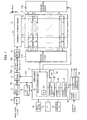
- Fig. 1 is a block diagram schematically illustrating a configuration of a plasma display (display device) which is an embodiment of the present invention.
- This plasma display 1 comprises a display panel (plasma display panel) 2, and an address electrode driver 16 and sustain electrode drivers 17A, 17B for driving the display panel 2.
- the address electrode driver 16 and sustain electrode drivers 17A, 17B make up a driver of the present invention.
- the plasma display 1 further comprises an A/D converter (ADC) 10; a signal processor 11; an SF data generator 13; a frame memory circuit 14; an APL detector (average peak level detector) 20; a controller 21; and a power supply circuit 28.
- ADC A/D converter
- the power supply circuit 28 generates operating voltages using externally supplied power and supplies the operating voltages to all processing blocks of the plasma display 1.
- the power supply circuit 28 incorporates a power consumption detector 29 for detecting the power consumption of the plasma display 1.
- the power consumption detector 29 supplies the detected power consumption to the controller 21.
- An input image signal is composed of R (red), G (green), B (blue) analog signals.
- the A/D converter 10 samples and quantizes the R, G, B analog signals, respectively, to generate 8-bit R, G, B digital image signals which are output to the signal processor 11.
- the signal processor 11 performs error diffusion processing and dither processing on the digital image signals from the A/D converter 10 to generate an image signal PD which is supplied to a multiplexer 12, controller 21, and APL detector 20.
- the signal processor 11 performs the error diffusion processing for diffusing the low two bits of an 8-bit image signal to the high six bits of each surrounding pixel to generate a 6-bit signal.
- the signal processor 11 further adds an element of a dither matrix to the 6-bit signal resulting from the error diffusion processing, generates a 4-bit image signal PD by bit-shifting the resultant signal, and supplies the 4-bit image signal.
- the multiplexer 12 superimposes display data from the controller 21 onto the image signal PD supplied from the signal processor 11 to generate a multiplexed image signal PDs which is output to the SF data generator 13.
- the SF data generator 13 generates SF data (sub-field data) GD based on the multiplexed image signal PDs according to the sub-field method, and outputs the SF data GD to the frame memory circuit 14.
- the frame memory circuit 14 temporarily stores the input SF data in an internal buffer memory (not shown), and reads SF data stored in the buffer memory and supplies the read SF data to the address electrode driver 16.
- the address electrode driver 16 generates address pulses based on the SF data input thereto, and supplies the address pulses to address electrodes D 1 - D m at a predetermined timing.
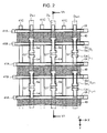
- the display panel 2 comprises: a plurality of discharge cells CL arranged in a matrix form; m (m is an integer equal to or larger than two) address electrodes D 1 , ..., D m extending in a Y-direction from the address electrode driver 16; (n+1) (n is an integer equal to or larger than two) sustain electrodes L 1 , ..., L n+1 extending in an X-direction perpendicular to the Y-direction from the first sustain electrode driver 17A; and n sustain electrodes S 1 , ... S n extending in a -X direction from the second sustain electrode driver 17B.
- the discharge cells CL are formed in respective regions near intersections of the address electrodes D 1 - D m with the sustain electrodes L 1 - L n+1 , S 1 - Sn.
- each of the sustain electrodes Sj, S j+1 (j is an integer from one to n-1) is composed of a flat bar-shaped bus electrode Sb extending in the -X direction, and a flat bar-shaped transparent electrodes Sa connected to the bus electrode Sb and extending in the Y-direction.
- the transparent electrode Sa which is made of a electrically conductive transparent material such as ITO (indium tin oxide), has T-shaped ends.
- the bus electrode Sb is made of a black or a dark metal film.
- Each of the sustain electrodes Lj, L j+1 is composed of a flat bar-shaped bus electrode Lb extending in the X-direction and made of a black or a dark metal film, and a flat bar-shaped transparent electrodes La connected to the bus electrode Lb and extending in the Y-direction.
- the transparent electrode La which is made of a electrically conductive transparent material such as ITO, has a T-shaped leading end opposing one leading end of the transparent electrode Sa across a discharge gap G1. As shown in Fig.
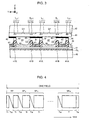
- these sustain electrodes S j , S j+1 , Lj, L j+1 are formed on the back of a transparent front substrate 42, and a front dielectric layer 43 is deposited to cover the sustain electrode Sj, S j+1 , Lj, L j+1 .
- a front dielectric layer 43 is deposited to cover the sustain electrode Sj, S j+1 , Lj, L j+1 .
- lightabsorbent dielectric layers (black stripes) 40 containing a black or a dark pigment extend in the X-direction in strip form.
- a protection film (not shown) made of MgO (magnesium oxide) is formed on the back of the front dielectric layer 43 and black stripes 40.
- each of the address electrodes D k-1 , D k , D k+1 is arranged to oppose a pair of transparent electrodes Sa, La in the Z-direction (depth direction of the front substrate 42).
- a back dielectric layer (protection layer) 45 is formed to cover these address electrodes D k-1 , D k , D k+1 for protection, and partitions (ribs) 41A, 41B, 41C, continuous over an X-Y plane, are disposed on the back dielectric layer 45.
- First partitions 41A are disposed in a stripe form along the X-direction beneath the bus electrodes Lb, respectively, while second partitions 41B are disposed in a stripe form along the X-direction beneath the bus electrodes Sb, respectively.
- a dielectric material 44 is stacked between the first partitions 41A and the black stripes 40.
- Third partitions 41C are disposed to define respective spaces above the address electrodes on the back dielectric layer 45 in the X-direction.
- the partitions (ribs) 41A, 41B, 41C form a main discharge space 60 between a pair of transparent electrodes La, Sa and the address electrode D k , and form a sub-discharge space 61 between the leading end of the transparent electrode Sa and the address electrode D k .
- the main discharge space 60 and the sub-discharge space 61 are in communication with each other through a gap G2 between the black stripe 40 and the second partition 41B.
- the main discharge space 60 and sub-discharge space 61 are filled with a discharge gas made of Xe (xenon) or the like which generates ultraviolet rays through a discharge.
- An electron emission layer 47 made of a secondary electron emission material having a relatively low work function, for example, MgO (magnesium oxide), BaO (barium oxide) or the like is formed on an inner wall exposed to the sub-discharge space 61.
- a fluorescent layer 48 is coated on an inner wall exposed to the main discharge space 60 for emitting red (R), green (G), or blue (B) light when it absorbs ultraviolet rays generated through a gas discharge.
- the discharge cell CL shown in Fig. 1 corresponds to an area defined by the first partitions 41A, 41A and third partitions 41C, 41C, and each discharge cell CL has one main discharge space 60 and one sub-discharge space 61.
- the foregoing description has been made of a structure of the display panel 2.
- the APL detector 20 detects an average peak level (APL) of an image signal transmitted from the signal processor 11 every field period or at intervals of a predetermined number of field periods, and supplies the detected average peak level to the controller 21.
- APL average peak level
- the detected average peak level is used for obtaining characteristic curve and ABL processing, as described later.
- the controller 21 comprises a driving control unit 22, a characteristic acquisition unit 24, a database 25, a power setting unit 26, and a power measuring unit 27, and is connected to an input device 30, an output interface unit (I/F) 31, and a wireless interface unit (wireless I/F) 32. Though not explicitly shown in the figure, the controller 21 can control the A/D converter 10, signal processor 11, multiplexer 12, SF data generator 13, frame memory circuit 14, and address electrode driver 16.
- the input device 30 comprises a key input device, a pointing device or the like, and can be used by a user to enter data such as numerical values.
- the input device 30 supplies to the controller 21 an input value from the user or a command corresponding to the input value.
- the output interface unit 31 is connected to an external device such as a media receiver, a set top box or the like, and has a function of outputting data supplied from the controller 21 to an external device connected thereto.
- the wireless interface unit 32 has a function of making a short-distance wireless communication with an external device, for example, a remote operation device such as a remote controller, via an infrared link.
- the driving control unit 22 controls the SF data generator 13, frame memory circuit 14, address electrode driver 16, first sustain electrode driver 17A, and second sustain electrode driver 17B in accordance with the image signal PD input from the signal processor 11 and the value of the detected average peak level supplied from the APL detector 20.
- the following description will be made of a gradation driving method implemented by the driving control unit 22.
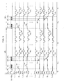
- Fig. 4 illustrates an example of a driving sequence for light emission.
- One field is divided into N (N is an integer equal to or larger than one) sub-fields SF 1 to SF N , each of which has an addressing period Tw and a light emission sustain period Ti.
- N is an integer equal to or larger than one
- sub-fields SF 1 to SF N each of which has an addressing period Tw and a light emission sustain period Ti.
- Only the first sub-field SF 1 has a reset period Tr immediately before the addressing period Tw, while only the last sub-field SF N has an erase period Te immediately after the light emission sustain period Ti.
- Fig. 5 is a timing chart schematically showing waveforms of pulses supplied to the display panel 2 in the reset period Tr, addressing period Tw, and light emission sustain period Ti.
- the first sustain electrode driver 17A supplies reset pulses RP L of positive polarity to the sustain electrodes L 1 , ..., L n+1 , respectively
- the second sustain electrode driver 17B supplies reset pulses RP S of negative polarity to the sustain electrodes S 1 , ..., S n , respectively
- the address electrode driver 16 supplies reset pulses RP D of positive polarity to the address electrodes D 1 , ..., D m , respectively.
- a gas discharge occurs in the discharge spaces 60, 61 between the transparent electrode Sa and the address electrode D k of the display panel 2 shown in Fig. 3, causing charges to be generated in the sub-discharge space 61.
- the charges move into the main discharge space 60 through the gap G2.
- a wall charge is accumulated on the surface of the fluorescent layer 48 of the main discharge space 60 in each of all the discharge cells CL.
- an erase addressing discharge is produced selectively in discharge cells CL to be turned off, to extinguish the wall charges.
- the second sustain electrode driver 17B sequentially supplies a scanning pulse SP of positive polarity to the address electrodes D 1 , ..., D m .
- the address electrode driver 16 sequentially supplies address pulses DP 1 , ..., DP n synchronized to the timing at which each scanning pulse SP is applied.
- the address electrode driver 16 supplies to the address electrodes D 1 - D m the address pulses DP 1 synchronized to the scanning pulse SP supplied to the sustain electrode S 1 on a first line, and then supplies the address electrodes D 1 - D m with the address pulses DP 2 synchronized to the scanning pulse SP supplied to the sustain electrode S 2 on a second line.
- the address electrode driver 16 repeatedly performs the foregoing processing until it supplies the address pulses DP n synchronized to the scanning pulse SP supplied to the sustain electrode S n on the last line.
- a gas discharge (erase addressing discharge) occurs in the space between the address electrode D k and the transparent electrode Sa shown in Fig. 3 in each of those discharge cells CL to be turned on. As a result, the wall charges accumulated in the discharge cells CL are extinguished.
- the first sustain electrode driver 17A repeatedly supplies discharge sustain pulses IP L of negative polarity to the sustain electrodes L 1 , ..., L n+1 , respectively, the number of times assigned thereto, while the second sustain electrode driver 17B repeatedly supplies discharge sustain pulses IP S of negative polarity to the sustain electrodes S 1 , ..., S n , respectively, the number of times assigned thereto.
- the amplitude of the last discharge sustain pulses IP E supplied to the sustain electrodes S 1 - S n is set to be slightly larger than that of the previous discharge sustain pulse IP S .
- a gas discharge occurs near a pair of transparent electrodes Sa, La in the main discharge space 60 shown in Fig. 3.
- the fluorescent layer 48 absorbs ultraviolet rays generated through this discharge, and excites to emit light in one of R, G, B.
- the erase addressing discharge is produced in the discharge cells CL to be turned off, to extinguish the wall charges.
- the sustain electrode drivers 17A, 17B repeatedly supply the discharge sustain pulses IP L , IP S as described above numbers of times assigned thereto.
- the processing is performed in the sub-fields SF 3 - SF N as shown in Fig. 4, and in the last erase period Te, the wall charges are extinguished by simultaneously producing erase discharges in all the discharge cells CL.
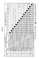
- Fig. 6 illustrates a relationship between gradation levels of image data PD S and the sub-fields SF 1 - SF 15 .
- the SF data generator 13 converts 4-bits of image data PDs supplied from the multiplexer 12 to 15-bits of SF data GD in accordance with a conversion table shown in Fig. 6, and outputs the SF data GD to the frame memory circuit 14.
- the least significant bit (LSB) of the SF data GD is set to “1,” and each of the remaining bits is set to “0.”
- the gradation level of the input data PDs is "k" (k is an integer from one to 14)
- a (k+1)-th bit of the SF data GD is set to “1,” and all the remaining bits are set to “0.”
- the gradation level of the input data PDs is "15,” all the bits from the least significant bit to the most significant bit (MSB) of the SF data are set to "0.”
- the address electrode driver 16 receives the SF data GD from the frame memory 14, samples and latches the SF data GD for one horizontal line, then generates an address pulse corresponding to the value of each bit of the image data GD, and supplies the address pulses to the address electrodes D 1 - D m .
- an erase addressing discharge occurs to extinguish the wall charges in those discharge cells CL to be turned off, in the addressing period Tw of the first sub-field SF 1 .
- a sustain discharge occurs in those discharge cells CL which have the wall charges, in each light emission sustain period Ti of the first to (k-1)-th sub-fields SF 1 - SF k-1 , and an erase addressing discharge occurs in the addressing period Tw of the k-th sub-field SF k .
- all the bits from the LSB to the MSB of the SF data GD have the value "0”
- a sustain discharge occurs in those discharge cells CL which have the wall charges, in each light emission sustain period Ti of all the sub-fields SF 1 - SF 15 , and no erase addressing discharge occurs in the addressing period Tw.
- the foregoing driving method is different from the driving method which sets ratios (weights) of light emission sustain periods assigned to each sub-field to a power of two, as described in the aforementioned Japanese Patent Kokai No. 2004-4606.
- the driving method of this embodiment employs a selective erase addressing method which only requires one time for each of the reset period Tr and erase period Te in each of the discharge cells CL in each field period (display period). Therefore, after the wall charges have been accumulated in all the discharge cells CL of the display panel 2 at the beginning of each field, the discharge cells CL will continue to emit light until the wall charges are erased by the erase addressing discharge, thereby advantageously preventing a pseudo contour when a moving image is displayed.
- the driving control unit 22 has the characteristic setting unit 23 which stores the characteristic representing a correspondence relationship between the average peak level (APL) and the number of occurrences of light emission (the number of times of supplying a discharge sustain pulse), i.e., a lookup table (characteristic table).
- the driving control unit 22 determines the number of discharge sustain pulses for each sub-field in accordance with the detected average peak level supplied from the APL detector 20 with reference to the lookup table set in the characteristic setting unit 23, and assigns the determined numbers of discharge sustain pulses to the sub-fields SF 1 - SF N (Fig. 4), respectively.
- the numbers of discharge sustain pulses assigned to the respective sub-fields SF 1 - SF N are stored in a register (not shown).
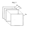
- the characteristic setting unit 23 stores lookup tables 50 1 , ..., 50 N corresponding to the respective sub-fields SF 1 , ..., SF N , as show in Fig. 7, so that the driving control unit 22 references a lookup table 50i corresponding to a sub-field SFi (i is an integer from one to N) when determining the number of discharge sustain pulses to be assigned to the sub-field SFi.
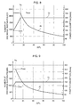
- Figs. 8 and 9 show examples of the relationship (ABL characteristic) between the average peak level and the number of discharge sustain pulses in the lookup table as described above.
- the horizontal axis of the graph corresponds to the average peak level (APL), while the left vertical axis of the graph corresponds to the number of discharge sustain pulses.
- a curve Pt is an ABL characteristic curve which represents the relationship between the APL and the number of discharge sustain pulses. It should be noted that the values of average peak levels in the graphs are normalized to have the value of "100" when all the discharge cells CL emit light at the highest gradation level, i.e., when the entire screen of the display panel 2 emits light at the highest peak luminance. Also, the right vertical axis of the graph corresponds to the power consumption (in Watts) of the plasma display 1.
- a curve Ct is a power characteristic curve representing a relationship between the APL and the power consumption.
- Fig. 8 illustrates an ABL characteristic when a target power consumption is set to 300 Watts (by default).
- the ABL characteristic curve Pt takes a substantially constant upper limit value Pmax in a region of the APL value from zero to S 0 , and monotonously decreases in a region of the APL value from S 0 to 100. In the initial region, the number of discharge sustain pulses is fixed at the upper limit value Pmax, while the power characteristic curve Ct monotonously increases.
- the power consumption (target power consumption) is fixed at 300 Watts, while the ABL characteristic curve Pt monotonously decreases under such limitations.
- the ABL characteristic curve in the default state has been previously measured and stored in a ROM or the like.
- Fig. 9 illustrates an ABL characteristic when the target power consumption is set to 200 Watt.
- the number of discharge sustain pulses of the ABL characteristic curve is fixed at the upper limit value Pmax, while the power characteristic curve Ct monotonously increases from the initial value Cmin to 200 Watts.
- the power consumption (target power consumption) of the power characteristic curve Ct is fixed at 200 Watts, while the ABL characteristic curve Pt monotonously decreases under such limitations.
- the database 25 stores lookup tables provided for each power consumption, and the characteristic acquisition unit 24 has a function of retrieving lookup tables 50 1 , ..., 50 N to be set in the characteristic setting unit 23 in accordance with the target power consumption specified by the power setting unit 26.
- the database 25 can store, for example, lookup tables (ABL characteristics) corresponding to the power consumptions of 300 Watts, 200 Watts, and 100 Watts, respectively.
- ABL characteristics lookup tables
- the characteristic acquisition unit 24 also has a function of calculating a lookup table corresponding to the target power consumption using lookup tables stored in the database 25 through interpolation.
- the characteristic acquisition unit 24 can interpolate an ABL characteristic curve Pt for 250 Watts using the ABL characteristic curve Pt for 300 Watts shown in Fig. 8 and the ABL characteristic curve Pt for 200 Watts shown in Fig. 9.
- the characteristic acquisition unit 24 can calculate the ABL characteristic curve Pt based on a basic function f(T;x) of the ABL characteristic which has been previously prepared and stored.
- the basic function f(T;x) relates to the target power consumption T and APL value x, and the functional shape of f(T;x) is uniquely determined by giving the target power consumption T.
- the characteristic acquisition unit 24 obtains a lookup table, i.e., the ABL characteristic curve Pt in accordance with the target power consumption specified by the power setting unit 26.
- the driving control unit 22 can assign the number of discharge sustain pulses for each of the sub-fields SF 1 - SF N to adjust the power consumption of the plasma display 1 to the target power consumption. Since the lookup tables are updated each time the target power consumption is specified, the power consumption of the plasma display 1 can be meticulously controlled in accordance with the situation.
- the user can directly enter or specify the value of target power consumption, for example, 300, 200, 180 or the like by operating on the input device 30 such as an operation panel provided on the plasma display 1.
- the input device 30 supplies these input values to the power setting unit 26 which sets the input value from the input device 30 as the target power consumption.
- the user can enter a value corresponding to the target power consumption instead of directly entering the value of the target power consumption by operating the input device 30.
- the input device 30 supplies to the power setting unit 26 a command corresponding to the depressed button, so that the power setting unit 26 sets the target power consumption in accordance with the command communicated from the input device 30.
- the user can enter a rate of change in the power consumption of the plasma display 1 by operating the input device 30, for example, 50 %, 40 %, 33 % or the like.
- the input device 30 supplies to the power setting unit 26 the value of the rate of change, or a command corresponding to the rate of change, and the power setting unit 26 calculates the target power consumption in accordance with the specified rate of change, and sets the calculated target power consumption. For example, when the rate of change (reduction rate) is specified to be 33 %, the target power consumption of 33 % is subtracted from the currently set target power consumption, and the resulting amount is set to a new target power consumption.
- the power supply circuit 28 comprises the power consumption detector 29 for detecting the amount of power consumed at each of the processing blocks in the plasma display 1, and supplies detected data to the power measuring unit 27.
- the power measuring unit 27 calculates the overall power consumption of the plasma display 1 based on the detected data supplied from the power consumption detector 29, and supplies the overall power consumption to the power setting unit 26.
- the power setting unit 26 can also subtract the rate of change in the power consumption from the power consumption of the plasma display 1 to set the resulting amount to the target power consumption.
- the value of the target power consumption set by the power setting unit 26 can be displayed on the display panel 2 or on a separate display unit independent of the display panel.
- the controller 21 outputs the value of the target power consumption set by the power setting unit 26, included in display data DD, to the multiplexer 12.
- the multiplexer 12 superimposes the display data DD onto an image signal PD input from the signal processor 11, thus displaying the value of the target power consumption on the display panel 2.
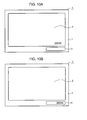
- Fig. 10A is a diagram showing an exemplary display of the value of the target power consumption. As shown in Fig. 10A, the target power consumption "200 W" can be displayed in a lower region of the display panel 2 on the front surface of the display panel 1.
- the plasma display 1 also has an auxiliary display unit 51 disposed in the housing 3, and can display the target power consumption on this auxiliary display unit 51.
- the controller 21 outputs the value of the target power consumption set by the power setting unit 26 to the auxiliary display unit 51 through the output interface unit 31, and can display the target power consumption "200 W" on the auxiliary display unit 51, as shown in Fig. 10B.
- the controller 21 can further output the value of the target power consumption to an external device through the output interface unit 31 or wireless interface unit 32 to display the target power consumption on a display unit provided in the external device.
- the target power consumption "200 W” can be displayed on a display unit 53 provided in a media receiver 52, as shown in Fig. 11, the value of the target power consumption can be wirelessly transmitted to a remote controller 54 to display the target power consumption "200 W” on a display unit 55 of the remote controller 54, as shown in Fig. 12, or the target power consumption "200 W” can be displayed on a display unit 57 provided in a power supply plug 56 connected to the power supply circuit 28 (Fig. 1), as shown in Fig. 13.
- the user can switch operating states of the display panel 2 and the display units 51, 53, 55, 57 from a target power consumption display state to a non-display state, and vice versa.
- a message, a character string, or a pattern may be displayed to permit the user to recognize the target power consumption.
- the power measuring unit 27 (Fig. 1) has a function of calculating the current power consumption of the plasma display 1 based on detected data supplied from the power consumption detector 29, and measuring the power consumption of the plasma display in units of predetermined periods, such as years, months, or days.
- the power measuring unit 27 also measures the power consumption during a standby state (standby power) when the main power supply of the plasma display 1 is shut off.
- the power measuring unit 27 further has a function of calculating the electric rate or electricity charges corresponding to the measured power consumption and storing the calculated electric rate in a memory (not shown).
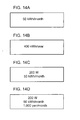
- the controller 21 can display the power consumption measured on a periodic basis, and the electric rate corresponding thereto on the display panel 2 and display units 51, 52, 53, 55, 57. For example, the controller 21 displays the power consumption "50 hWh/month” for one month as shown in Fig. 14A; the power consumption "400kWh/year” for one year as shown in Fig. 14B; the current power consumption "200 W” in parallel with the power consumption "50 kWh/month” for one month as shown in Fig. 14C; or the current power consumption "200 W” in parallel with the power consumption "50 kWh/month” for one month and the corresponding electric rate "1,000 yens/month.”
- the unit price used by the power measuring unit 27 for calculating the electric rate (for example, the electric rate per 1kWh) can be set by the user. Also, the user can reset the power consumption measured on a periodic basis and can reset the electric rates to their initial values.
- the user can readily view the target power consumption set by operating the input device 30, and can therefore know the power consumption of the plasma display 1 in a simple manner. It is therefore possible to provide the plasma display 1 which can permit the user to realize a reduction in power consumption and can support the power saving in consideration of the earth environment.
Landscapes
- Engineering & Computer Science (AREA)
- Physics & Mathematics (AREA)
- Power Engineering (AREA)
- Plasma & Fusion (AREA)
- Computer Hardware Design (AREA)
- General Physics & Mathematics (AREA)
- Theoretical Computer Science (AREA)
- Control Of Indicators Other Than Cathode Ray Tubes (AREA)
- Transforming Electric Information Into Light Information (AREA)
- Control Of Gas Discharge Display Tubes (AREA)
- Control Of El Displays (AREA)
Applications Claiming Priority (2)
| Application Number | Priority Date | Filing Date | Title |
|---|---|---|---|
| JP2004138403A JP2005321508A (ja) | 2004-05-07 | 2004-05-07 | ディスプレイ装置 |
| JP2004138403 | 2004-05-07 |
Publications (2)
| Publication Number | Publication Date |
|---|---|
| EP1594114A2 true EP1594114A2 (de) | 2005-11-09 |
| EP1594114A3 EP1594114A3 (de) | 2009-09-16 |
Family
ID=34936167
Family Applications (1)
| Application Number | Title | Priority Date | Filing Date |
|---|---|---|---|
| EP05009820A Withdrawn EP1594114A3 (de) | 2004-05-07 | 2005-05-04 | Anzeigegerät |
Country Status (3)
| Country | Link |
|---|---|
| US (1) | US7592974B2 (de) |
| EP (1) | EP1594114A3 (de) |
| JP (1) | JP2005321508A (de) |
Families Citing this family (9)
| Publication number | Priority date | Publication date | Assignee | Title |
|---|---|---|---|---|
| JP2006091681A (ja) * | 2004-09-27 | 2006-04-06 | Hitachi Displays Ltd | 表示装置及び表示方法 |
| JP2007156045A (ja) * | 2005-12-05 | 2007-06-21 | Sony Corp | 自発光表示装置、消費電力検出装置及びプログラム |
| JP4666033B2 (ja) * | 2008-09-09 | 2011-04-06 | ソニー株式会社 | 情報処理装置、およびプログラム |
| JP5134508B2 (ja) | 2008-11-19 | 2013-01-30 | 株式会社日立製作所 | テレビジョン装置 |
| US8970705B2 (en) * | 2009-03-20 | 2015-03-03 | Sony Corporation | Graphical power meter for consumer televisions |
| KR101708028B1 (ko) * | 2010-04-13 | 2017-02-20 | 삼성전자주식회사 | 소비 전력 표시 방법 및 장치 |
| KR101679360B1 (ko) * | 2010-08-05 | 2016-11-25 | 삼성디스플레이 주식회사 | 계조전압 생성장치 및 방법, 및 유기전계발광표시장치 |
| FR3073302A1 (fr) * | 2017-11-08 | 2019-05-10 | STMicroelectronics (Grand Ouest) SAS | Procede et dispositif de surveillance d'au moins une activite d'un objet connecte |
| US12210609B2 (en) | 2021-10-29 | 2025-01-28 | Stmicroelectronics Application Gmbh | Central controller for multiple development ports |
Family Cites Families (35)
| Publication number | Priority date | Publication date | Assignee | Title |
|---|---|---|---|---|
| US4700188A (en) * | 1985-01-29 | 1987-10-13 | Micronic Interface Technologies | Electric power measurement system and hall effect based electric power meter for use therein |
| KR930006419B1 (ko) * | 1990-10-26 | 1993-07-14 | 삼성전자 주식회사 | 재편성원격제어송신기의 모드전환 및 표시방법 |
| JP2856241B2 (ja) * | 1993-11-17 | 1999-02-10 | 富士通株式会社 | プラズマディスプレイ装置の階調制御方法 |
| US5745085A (en) * | 1993-12-06 | 1998-04-28 | Fujitsu Limited | Display panel and driving method for display panel |
| US5696501A (en) * | 1994-08-02 | 1997-12-09 | General Electric Company | Method and apparatus for performing the register functions for a plurality of metering devices at a common node |
| JPH08314618A (ja) * | 1995-05-23 | 1996-11-29 | Canon Inc | 電力残量報知機能付き軌跡入出力装置 |
| US5870685A (en) * | 1996-09-04 | 1999-02-09 | Ericsson Inc. | Mobile station operations management based on battery capacity |
| ES2121560B1 (es) * | 1997-05-08 | 1999-08-16 | Sala Vicente Rodilla | Avisador programable de consumo electrico. |
| JP3928679B2 (ja) * | 1998-02-27 | 2007-06-13 | 東芝キヤリア株式会社 | 空気調和機 |
| US6591084B1 (en) * | 1998-04-27 | 2003-07-08 | General Dynamics Decision Systems, Inc. | Satellite based data transfer and delivery system |
| JP2000162255A (ja) * | 1998-11-26 | 2000-06-16 | Aiwa Co Ltd | 電子機器 |
| JP3477520B2 (ja) * | 1999-04-21 | 2003-12-10 | 松下電器産業株式会社 | 移動体通信装置、通信システム、及び通信方法 |
| JP3438693B2 (ja) * | 2000-02-03 | 2003-08-18 | 日本電気株式会社 | 表示部付き電子機器 |
| JP2001343142A (ja) * | 2000-06-01 | 2001-12-14 | Funai Electric Co Ltd | 空気調和機の運転条件制御装置 |
| US6618837B1 (en) * | 2000-09-14 | 2003-09-09 | Cadence Design Systems, Inc. | MOSFET modeling for IC design accurate for high frequencies |
| US6762741B2 (en) * | 2000-12-22 | 2004-07-13 | Visteon Global Technologies, Inc. | Automatic brightness control system and method for a display device using a logarithmic sensor |
| JP2002297715A (ja) * | 2001-03-30 | 2002-10-11 | Minolta Co Ltd | 情報処理装置、情報処理方法、画像処理システム、画像処理装置、監視装置、監視方法、消費電力表示方法、プログラム及び記録媒体 |
| US6809711B2 (en) * | 2001-05-03 | 2004-10-26 | Eastman Kodak Company | Display driver and method for driving an emissive video display |
| JP2002354510A (ja) * | 2001-05-30 | 2002-12-06 | Matsushita Electric Ind Co Ltd | 消費電力表示装置 |
| JP4698070B2 (ja) * | 2001-06-07 | 2011-06-08 | パナソニック株式会社 | プラズマディスプレイパネルの駆動方法及びプラズマディスプレイ装置 |
| JP4004247B2 (ja) * | 2001-07-09 | 2007-11-07 | 三洋電機株式会社 | 音響装置 |
| JP4707887B2 (ja) * | 2001-07-11 | 2011-06-22 | パナソニック株式会社 | 表示制御装置及び表示装置 |
| JP4180828B2 (ja) * | 2002-01-18 | 2008-11-12 | パイオニア株式会社 | プラズマディスプレイパネルの駆動方法及び駆動装置 |
| EP1316938A3 (de) * | 2001-12-03 | 2008-06-04 | Pioneer Corporation | Steuerverfahren für einen Plasmabildschirm |
| JP2003195988A (ja) * | 2001-12-25 | 2003-07-11 | Sharp Corp | 消費電力管理装置およびその方法 |
| JP2003219987A (ja) * | 2002-01-31 | 2003-08-05 | Matsushita Electric Ind Co Ltd | 暖房便座及び温水洗浄便座 |
| JP2003222402A (ja) * | 2002-01-31 | 2003-08-08 | Matsushita Electric Ind Co Ltd | 電気機器 |
| JP3856705B2 (ja) * | 2002-02-07 | 2006-12-13 | 大阪瓦斯株式会社 | エネルギ使用量削減評価方法、エネルギ使用量削減評価システム、エネルギ使用量削減評価装置、コンピュータプログラム及び記録媒体 |
| US7149636B2 (en) * | 2002-04-04 | 2006-12-12 | Texas Instruments Incorporated | Method and apparatus for non-obtrusive power profiling |
| JP4064268B2 (ja) | 2002-04-10 | 2008-03-19 | パイオニア株式会社 | サブフィールド法を用いた表示装置及び表示方法 |
| JP2004023283A (ja) * | 2002-06-13 | 2004-01-22 | Kojima Co Ltd | 家電制御装置、家電制御方法及びプログラム |
| JP2004037822A (ja) * | 2002-07-03 | 2004-02-05 | Fuji Photo Film Co Ltd | 電池残量警告装置 |
| EP1437705A1 (de) * | 2003-01-10 | 2004-07-14 | Deutsche Thomson-Brandt Gmbh | Verfahren zur Optimierung der Helligkeit in einer Anzeigevorrichtung und Anordnung zur Durchführung des Verfahrens |
| US7580033B2 (en) * | 2003-07-16 | 2009-08-25 | Honeywood Technologies, Llc | Spatial-based power savings |
| US7805243B2 (en) * | 2003-08-05 | 2010-09-28 | Northrop Grumman Corporation | Personal digital assistant having satellite communications capacity |
-
2004
- 2004-05-07 JP JP2004138403A patent/JP2005321508A/ja active Pending
-
2005
- 2005-05-04 EP EP05009820A patent/EP1594114A3/de not_active Withdrawn
- 2005-05-06 US US11/123,212 patent/US7592974B2/en not_active Expired - Fee Related
Also Published As
| Publication number | Publication date |
|---|---|
| US7592974B2 (en) | 2009-09-22 |
| US20050264482A1 (en) | 2005-12-01 |
| EP1594114A3 (de) | 2009-09-16 |
| JP2005321508A (ja) | 2005-11-17 |
Similar Documents
| Publication | Publication Date | Title |
|---|---|---|
| US5745085A (en) | Display panel and driving method for display panel | |
| US6369782B2 (en) | Method for driving a plasma display panel | |
| KR100825164B1 (ko) | 플라즈마 디스플레이 장치의 구동 방법 및 플라즈마디스플레이 장치 | |
| JP2004021181A (ja) | プラズマディスプレイパネルの駆動方法 | |
| KR20050100338A (ko) | 표시 장치 | |
| US7592974B2 (en) | Display device | |
| KR100721045B1 (ko) | 표시 패널의 구동 방법 및 구동 장치 | |
| JP2006003398A (ja) | プラズマディスプレイパネルの駆動方法 | |
| US8395645B2 (en) | Plasma display device and drive method of plasma display panel | |
| JP2004310044A (ja) | アドレス駆動部の保護機能を有する映像ディスプレイ装置 | |
| JP4541025B2 (ja) | 表示パネルの駆動方法 | |
| JP2003271092A (ja) | プラズマディスプレイパネルの駆動方法およびプラズマディスプレイ装置 | |
| JP2003140605A (ja) | プラズマ表示装置及びその駆動方法 | |
| JPH1152913A (ja) | プラズマディスプレイ装置 | |
| US7561153B2 (en) | Apparatus and method of driving plasma display panel | |
| KR100625542B1 (ko) | 플라즈마 표시 패널의 구동장치 및 구동방법 | |
| JP2007148411A (ja) | プラズマディスプレイ装置及びその駆動方法 | |
| US7391392B2 (en) | Method and device for driving display panel unit | |
| US20060125726A1 (en) | Plasma display apparatus | |
| US20090201276A1 (en) | Driving method of a plasma display device and a plasma display device | |
| JP3606861B2 (ja) | Ac型pdpの駆動方法 | |
| KR100667241B1 (ko) | 플라즈마 디스플레이 장치 | |
| KR100634696B1 (ko) | 플라즈마 디스플레이 패널의 구동 장치 및 방법 | |
| US8154477B2 (en) | Plasma display apparatus including a driver supplying a signal to a scan electrode during a reset period | |
| JP2009192647A (ja) | プラズマディスプレイ装置およびプラズマディスプレイパネルの駆動方法 |
Legal Events
| Date | Code | Title | Description |
|---|---|---|---|
| PUAI | Public reference made under article 153(3) epc to a published international application that has entered the european phase |
Free format text: ORIGINAL CODE: 0009012 |
|
| AK | Designated contracting states |
Kind code of ref document: A2 Designated state(s): AT BE BG CH CY CZ DE DK EE ES FI FR GB GR HU IE IS IT LI LT LU MC NL PL PT RO SE SI SK TR |
|
| AX | Request for extension of the european patent |
Extension state: AL BA HR LV MK YU |
|
| PUAL | Search report despatched |
Free format text: ORIGINAL CODE: 0009013 |
|
| AK | Designated contracting states |
Kind code of ref document: A3 Designated state(s): AT BE BG CH CY CZ DE DK EE ES FI FR GB GR HU IE IS IT LI LT LU MC NL PL PT RO SE SI SK TR |
|
| AX | Request for extension of the european patent |
Extension state: AL BA HR LV MK YU |
|
| RAP1 | Party data changed (applicant data changed or rights of an application transferred) |
Owner name: PANASONIC CORPORATION |
|
| AKX | Designation fees paid |
Designated state(s): DE FR GB |
|
| STAA | Information on the status of an ep patent application or granted ep patent |
Free format text: STATUS: THE APPLICATION IS DEEMED TO BE WITHDRAWN |
|
| 18D | Application deemed to be withdrawn |
Effective date: 20100316 |