EP1593146B1 - Strahlungs-wärme-quelle - Google Patents
Strahlungs-wärme-quelle Download PDFInfo
- Publication number
- EP1593146B1 EP1593146B1 EP04709941A EP04709941A EP1593146B1 EP 1593146 B1 EP1593146 B1 EP 1593146B1 EP 04709941 A EP04709941 A EP 04709941A EP 04709941 A EP04709941 A EP 04709941A EP 1593146 B1 EP1593146 B1 EP 1593146B1
- Authority
- EP
- European Patent Office
- Prior art keywords
- radiant
- heating elements
- reflector
- source
- workpiece
- Prior art date
- Legal status (The legal status is an assumption and is not a legal conclusion. Google has not performed a legal analysis and makes no representation as to the accuracy of the status listed.)
- Expired - Lifetime
Links
Images




Classifications
-
- H—ELECTRICITY
- H10—SEMICONDUCTOR DEVICES; ELECTRIC SOLID-STATE DEVICES NOT OTHERWISE PROVIDED FOR
- H10P—GENERIC PROCESSES OR APPARATUS FOR THE MANUFACTURE OR TREATMENT OF DEVICES COVERED BY CLASS H10
- H10P95/00—Generic processes or apparatus for manufacture or treatments not covered by the other groups of this subclass
- H10P95/90—Thermal treatments, e.g. annealing or sintering
-
- H—ELECTRICITY
- H10—SEMICONDUCTOR DEVICES; ELECTRIC SOLID-STATE DEVICES NOT OTHERWISE PROVIDED FOR
- H10P—GENERIC PROCESSES OR APPARATUS FOR THE MANUFACTURE OR TREATMENT OF DEVICES COVERED BY CLASS H10
- H10P72/00—Handling or holding of wafers, substrates or devices during manufacture or treatment thereof
- H10P72/04—Apparatus for manufacture or treatment
- H10P72/0431—Apparatus for thermal treatment
- H10P72/0436—Apparatus for thermal treatment mainly by radiation
-
- H—ELECTRICITY
- H10—SEMICONDUCTOR DEVICES; ELECTRIC SOLID-STATE DEVICES NOT OTHERWISE PROVIDED FOR
- H10P—GENERIC PROCESSES OR APPARATUS FOR THE MANUFACTURE OR TREATMENT OF DEVICES COVERED BY CLASS H10
- H10P95/00—Generic processes or apparatus for manufacture or treatments not covered by the other groups of this subclass
Definitions
- the invention relates to a heating source and more particularly to a heating source used in heating a workpiece such as a semiconductor wafer or similar object and more particularly to temperature dependent processes where the workpiece is heated with a heat radiating source.
- the speed of several types of semiconductor wafer processing depends on a process gas active ingredient concentration or delivery rate at the region of the wafer surface and also on the substrate temperature maintained at the wafer surface.
- a goal of treatment systems is to provide uniform temperature and active ingredients distributions across the wafer process area. In certain circumstances it is also important to maintain control over these process parameters during a temperature ramping period of a treatment process.
- the heating and process gas delivery are under control of separate process tool components and depend on the geometry and construction of the processing unit.
- Prior art heating and gas delivery components of a wafer processing system have been limited in achieving time and surface uniformity of action.
- the speed at which the temperature dependent process reaction takes place can be different at different wafer locations.
- This phenomenon is generally referred to as process non-uniformity.
- the process non-uniformity can result in overexposure to plasma with the subsequent damage of the wafers and other negative effects.
- the non-uniformity slows the resist cleaning speed and therefore causes a decrease of wafer throughput of the stripping process.
- process volumes or chambers are basically symmetric about a center axis, as is the wafer.
- the processes parameters applied to the wafer such as heating and the active plasma ingredient delivery should also be symmetric about the wafer axis.
- the boundary conditions for gas/species distribution and for heat exchange process on the wafer surface boundary also tend to be of rotationally symmetric about the axis. Therefore the process and temperature non-uniformity may be considered as a superposition of a radial and azimuthal components.
- the radial component of process non-uniformity is measured along the wafer radius. This component in particular is a result of incomplete mutual compensation of the temperature and plasma concentration across a wafer diameter. For example, a lower temperature in the center of the wafer would be needed to compensate for a higher plasma species activity at the center area of the wafer. If the heater design cannot compensate enough or overcompensates, a radial process non-uniformity results.
- An azimuth component of process non-uniformity is measured as a degree of process speed deviation along a specified circumference on the wafer surface.
- This component of non-uniformity is mostly a result of a local asymmetry that is specific to the process chamber/gas supply system design or is produced by different tolerances in the system. For example, such asymmetry may be due to gas flow asymmetry at a chamber door zone or a difference in individual heating elements intensity or excessive tolerance of a radiant heater bulb filament position and (or) or bulb base mounting orientation.
- process gas supply and process gas exhaust design for downstream microwave ashers can cause substantial radial and azimuth non-uniformity in active species delivery.
- the radial process non-uniformity component resulting from radial non-uniformity of temperature and radial non-uniformity of the active species delivery for a design that are basically symmetric with respect of the wafer axis could be mutually compensated. Developing of the heating sources with more flexibility in optimization of heat distribution over the wafer surface becomes important in achieving the required compensation.
- Uniform Heating and Uniform Temperature are used to specify the degree of difference between the actual temperature and heat rate radial distribution compared to the distribution required for ideal compensation of the non-uniform radial plasma activity, mentioned above.
- Process Uniformity and Azimuthal Uniformity of Heating and Temperature are applied in their original sense i.e. as degree of deviation from the corresponding statistically averaged values.
- the system disclosed in the '555 patent also exhibits certain problems.
- the elliptical reflector in combination with a tubular reflector creates strong local process speed dependence on individual parameters and space orientation for each set of bulb/reflector. This is because the radiant energy of each set is concentrated by individual reflectors in relatively narrow areas of the target positioned with respect to each set.
- This prior art arrangement can result in azimuthal and especially radial non-uniformity of the temperature and, therefore, processes speed non-uniformity.
- An additional source of non-uniformity is inconsistency of an individual reflector's shape, finish quality, position and orientation due to dimensional tolerances of the reflector's and bulb mountings.
- the numerous manufacturing and assembly tolerances also include individual bulb intensity, filament spatial position, reflectors and bulbs base installation that can result in non-uniformity of temperature and therefore, processing rate.
- tubular or pan-shaped reflectors Another problem with tubular or pan-shaped reflectors is loss of part of the bulb energy which is directed parallel or close to parallel to the wafer plane. This part of the radiant energy is absorbed by other bulbs and numerous back and force reflections with partial absorbtion on the reflector surfaces before the radiant energy leave the heater in the wafer direction. The total heating effectiveness of such an array drops due to the absorbed energy lost without heating the wafer.
- the heating elements are positioned by plugging in electrical sockets, which are in turn attached to the reflector assembly. Additional to these tolerances that generate hearting non-uniformity, is a bulb base to electrical socket position tolerance.
- EP1100114 discloses a temperature control system for a plasma processing device, the plasma processing device comprises a plasma generator and a processing chamber in communication with the plasma generator such that plasma within the generator may pass into the camber and react with the surface of a substrate residing therein.
- the temperature control system comprises (i) a radiant heater assembly for heating the substrate, comprising a plurality of radiant heating elements arranged in a plurality of zones, each zone comprising at least one heating element, and a focused reflector for focusing radiant energy from the heating elements toward the substrate; (ii) a feedback mechanism for providing a substrate temperature feedback signal; and (iii) a controller, including a P-I-D closed loop controller and a lamp power controller.
- the P-I-D closed loop controller receives a temperature setpoint signal and the temperature feedback signal and the temperature feedback signal and in response thereto independently adjusts a control variable sent to the lamp power controller.
- the power controller (90) then adjusts the power applied to the plurality of zones of radiant heating elements, independently of the control variable, based on temperature zone maps stored in processor memory.
- the power controller operates in at least a first ramp state and a second steady state, depending upon the magnitude of difference between the temperature setpoint signal and the temperature feedback signal.
- US5418885 describes a three zone rapid thermal processing system includes three arrays of radiant heating lamps for heating a semiconductor wafer.
- the arrays are positioned along the axis of the wafer such that one array is adjacent one face of the wafer, the second array is adjacent the second face of the wafer and the third array is adjacent the edge of the water.
- a wafer holder holds the wafer face transverse to the common axis of the radiant heating lamps. Reflectors at each array reflect radiant heat onto the wafer.
- the arrays are independently connected to power sources and a controller to provide efficient coupling of the heat sources and a uniform temperature distribution across a wafer.
- US4891499 describes a silicon semiconductor wafer is places in a vacuum chamber device side facedown.
- Laser beams of equal power are directed at an edge point and a center point of the wafer.
- the laser beams are reflected from the edge point and the center point into first and second infrared photo detectors.
- a differential amplifier evaluates the reflected laser beams for a power difference and signals a current source.
- Current source heats a quartz ring which surrounds the wafer. The quartz ring passes the hear to the wafer until the amplifier no longer senses a power difference, which is indicative of an equal wafer surface temperature.
- EP0981153 describes a radiant heating apparatus for reducing the cumulative temperature gradient over a semiconductor workpiece during a low temperature process is comprised of a plurality of reflecting units, wherein each reflecting unit is comprised of a back reflector (2), a tubular reflector extending from the back reflector towards the workpiece (32, 34, 36), and a radiant energy source disposed in the tubular reflector in front of the back reflector (10), wherein a cross section of the tubular reflector is in the shape of a truncated segment of a circle.
- a radiant source for heating a workpiece comprising: a plurality of radiant heating elements arranged in a single array that is generally concentric about a source centre axis; and a reflector having a reflecting surface that bounds a single channel which opens in a direction of a workpiece and that contains the heating elements of said single array, said reflector comprising inner, outer and bottom walls that extend around at least a portion of the centre axis to define said single channel and that are surface finished for reflecting radiant energy emitted by the heating elements to a region occupied by the workpiece; the bottom wall of said single channel comprising a part of a plane and said inner and outer walls comprising a part of a cone surface of revolution spanning two or more adjacent heating elements such that said single channel widens outwardly toward the workpiece to reflect radiant energy toward the workpiece; wherein the heating elements each comprise a centre axis that is orientated at an angle with respect to a central
- a method according to claim 13 for use in heating a workpiece comprising: providing a radiant heat reflector having a reflecting surface that forms a single channel that extends around at least a portion of a centre axis wherein the reflecting surface includes inner and outer walls that form a part of a cylinder and/or a cone and/or a convex curve surface of revolution that widens outwardly toward a workpiece region; mounting a plurality of radiant heating elements within the single channel of the reflector in an array that is generally concentric about the centre axis such that the walls of the single channel span two or more adjacent heating elements to reflect radiant energy toward a workpiece region such that said radiant heating elements are disposed at an angle with respect to a central axis of the single array; and controllably energizing the heating elements to emit radiant energy from the heating elements for directing radiant energy to the workpiece region.
- the present invention thus provides a radiant heating device with high consistency of heating conditions in both a radial and an azimuth orientation across a plane of a workpiece such as a wafer.
- Use of a reflective inner wall and angled radiant energy bulbs combined with an optimised shape of the inner and out wall and bottom reflecting surfaces (in one embodiment the radiant heating device is oriented to have what can be referred to as a bottom surface) provide uniform heat distribution over a wafer surface with a more compact design.
- a radiant heater constructed in accordance with one embodiment of the invention results in more uniform processing parameters across the wafer surface as well as more uniform process speed and heating effectiveness.
- the reflector structure involves plane surfaces and/or simple surfaces of revolution shaped to provide a better uniformity of process conditions and highly effective energy use.
- the relatively flat non-focusing planar, cone, cylindrical or convex curved reflecting surfaces reflect heat energy from a group of or all of the heating elements and do not focus an individual bulb's energy at the workpiece region.
- a convex (as seen from a position of the heating elements) internal wall disperses energy of each bulb to the even wider area of wafer surface and makes heat delivered to the wafer from each bulb smoother, less concentrated.
- the effect is opposite to the focusing property of prior art parabolic or elliptical or similar, concave (as seen from a position of the elements) surfaces, including cylinder outer wall type design. Energy from each individual bulb reflected from prior art concave surface is concentrated at a smaller area of the wafer and equalizing participation of other bulbs at this concentrated area is less.
- a defocusing effect can be made even stronger if outer wall reflecting surface is made to be convex (as seen from a position of the heating elements).
- a convex outer wall portion formed from a curved line rotated about a center axis is used. This effect could also be used on a bottom and on inner surfaces of revolution, adding (as seen from the position of the bulbs) more convexity in direction perpendicular to the natural convexity of the inner cylinder or cone. This produces additional defocusing or divergence of radiative heat reflected on the bottom and outer wall reflecting surfaces.
- an internal reflecting wall in addition to commonly used outer and bottom reflecting surfaces results in a reflector shape that is like a two-wall channel which may or may not have a well defined bottom reflecting surface.
- the internal wall serves as additional feature giving more flexibility in the bulbs radiation redirection.
- Use of the term "walls" and "bottom” is to describe one exemplary embodiment wherein the workpiece is positioned horizontally above the heating source. It is appreciated, however, that the invention has utility in other orientations and suitable terminology would be substituted in describing the invention with its components in alternative orientations.
- An exemplary embodiment includes a channel type reflecting surface that diminishes the individual and group assembly tolerances that can effect heating target temperature uniformity. At least some of the reflecting surface is defined by a surface of revolution around the heater axis.
- the channel reflector's cross-section shape combines straight lines and curved lines selected to produce a specific distribution of radiant heat intensity over the wafer surface for specified applications.
- the shape of the surfaces of revolution above can be approximated with an inscribed polyhedron surface where the number of faces, for example, may be equal to the number of heating elements.
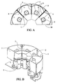
- FIG. A is a plan view of a prior art radiant lamp array for wafer heating in semiconductor processing chambers.
- FIG. B shows a perspective view of the apparatus of FIG A.
- These depictions are similar to depictions shown in US patent no. 6,023,555 to Penelon et al .
- the '555 patent is incorporated herein by reference.
- one half of an array of heating elements of sources is shown, the second half which is not shown is symmetric to the part shown in FIG.s A and B.
- In the plan view of the FIG. A are also shown four of the eight individual heating elements 1. As described in the '555 patent they are quartz halogen bulbs.
- FIG.s A and B also depict ellipsoidal shaped back reflectors 2 combined with the adjacent tubular reflectors 3 which have reflector surfaces that extend in a direction parallel to an elongated axis of an associated heating lamp.
- Each of the ellipsoidal and tubular reflectors is mounted next to an associated a single bulb heating element to act as an individual concentrator of radiant energy in the direction of a semiconductor wafer.
- the prior art reflectors 2,3 shown in FIG.s A and B achieve relatively strong radiant energy focusing at the wafer surface in the vicinity of the reflector's associated bulb.
- the superposition of the heat delivered to the wafer from other lamps in the array of lamps shown in FIG. A is minimized.
- Individual tolerances in bulb power, filament and reflector position are pronounced or relatively high due to the focusing effect of the individual reflectors in adjacent to corresponding bulb wafer area. Sufficient radial and especially azimuth uniformity is very difficult to achieve by such an arrangement.
- tubular reflectors of the prior art and any pan-shaped reflector not having an internal reflecting wall introduces a loss of radiant energy because they function similar to a black body.
- Energy from the bulbs which is directed parallel or nearly parallel to the plane of the wafer plane experiences numerous reflections before it leaves the reflector.
- the numerous reflections causes unavoidable heat loss due to absorption on the reflector walls so that some of the power output from the radiant source is wasted.
- each bulb is plugged into electrical socket, which in turn is fastened to a base of the apparatus.
- the reflectors 2 are fastened to mounting brackets 5 that are independent from the bulb mounting base.
- the accurate filament- reflector- mutual position and each of them - position relatively to heating target is difficult to provide. This is an additional source of wafer temperature and therefore ash rate non-uniformity.
- FIG. 1A illustrates a radiant energy source 110 for heating a semiconductor wafer 112 ( FIG. 5 ) positioned relative to the source 110.
- the radiant energy source includes a plurality of radiant heating elements 120 arranged in an array that is generally concentric about a source center axis 122.
- the source 110 also includes a base 130 constructed from a machined aluminum body that defines a two-wall channel or cavity 132 that bounds the heating elements from all directions except the direction of the wafer. Exterior and interior channel walls 134 that bound the cavity along inside and outside walls and in the illustrated embodiment extend completely around the center axis 122 reflect radiant energy emitted by the heating elements 120 to a region occupied by a wafer 112.
- at least some of the walls are defined by a cylinder and/or a cone surface formed by revolving a line about the center axis 122.
- the exemplary embodiment of the invention is formed by two symmetric body halves 131a, 131b that together form the base 130.
- a two half design is suitable for downstream plasma ashers aligned with the bottom center position of the process exhaust line. In other cases the one- piece design is more suitable and cheaper to manufacture.
- the reflecting surfaces that bound the cavity include a bottom plane wall 134a, an outer wall made from a combination of a generally vertical cylinder outer wall 134b and cone shaped wall 134d, a cone shaped inside wall 134c, and upper back reflecting cone surface 134e.
- the surface 134e defines a lip having an overhang that reflects radiation back toward the region of the bulb. This lip allows radiation which otherwise would miss the target to be returned to the region of the channel so that energy reflects again from the reflector surfaces and is redirected back to the wafer.
- the feature is important for creating an effective compact heater of higher power, that allows an increase in wafer heating speed and therefore improves the tool's productivity. If more bulbs are used, in order to achieve this goal, the heater and heater output optical diaphragm generally become larger and may exceed the wafer size. Without the returning lip, part of energy directed out of the heater will miss the wafer area and cause loss of energy and reduce the effectiveness of the heating source. Use of a larger number of bulbs causes the energy loss to be greater.
- the lip shape is not necessarily a cone and may be optimized for uniformity requirements.
- the lip's internal diameter is most preferably selected to return all the rays which otherwise miss the wafer. Use of the lip application is then more effective than if the reflector's optical diaphragm is larger than the wafer.
- the walls 134a -134e are plate coated with a gold finish that reflects heat from these walls with a high efficiency.
- the reflector walls shown in the FIG.s are coaxial with the axis 122 and as was mentioned, define an inner, outer and bottom surfaces of the reflecting channel that bounds the bulbs pattern on three sides, excluding the direction facing the wafer. More than one generally circular array of bulbs positioned around the same axis could be used within the reflecting channel, for example for larger wafer size machines or in a case of smaller bulbs applied.
- the heating elements 120 include an elongated bulb 138 ( FIG. 9 ) having a center axis that is oriented at an angle A1 ( FIG. 6 ) with respect to the array's center axis 122.
- an elongated bulb 138 FIG. 9
- the aluminum body halves 131a, 131b are water-cooled by mean of running water through channels 135 made in the reflector body.
- the elongated bulb 138 of each of the heating elements 120 is oriented by a passageway or opening 140 ( Fig. 8A ) that extends from a bottom in one of the two halves 131a, 131b and extends upwardly to meet the reflecting cavity/channel 132 in the base 130.
- the heating elements 120 include halogen bulbs 138 that are commercially available as part no. J1H240V-1000WCH from USHIO. These bulbs are mechanically fastened to the reflector base by means of an intermediate bushing 150 ( FIG. 9 ).
- the bushing 150 is made from high thermal conductivity material such as aluminum to transmit heat away from the bulb seal in order to prevent its overheating.
- the bushing 150 defines a slot that extends through a body of the bushing to accommodate a base 154 of the bulb.
- the orientation of the bulb is fixed by a screw 156 that passes through an opening 158 in the bushing so that the bulb's base is slipped into the bushing and the screw is tightened to engage the base thereby fixing the orientation and position of the bulb 138.
- Contact pins 160 that extend from the base 154 engage a socket 152 and circuitry coupled to the socket for controllably energizing the bulb 138.
- the electrical sockets 152 are attached to the bulbs independently of the bulb support provided by the bushing 150 and do not affect the bulb orientation. This separate mounting helps avoid the extra long dimensional tolerance chain needed to align each bulb filament relatively to the wafer.
- the disclosed mounting arrangement therefore improves the temperature uniformity of the wafer and in turn- process performance uniformity.
- the specific bulb distance from the array center axis 122, the angle A1 between a center axis of a given bulb 120a to the array center axis 122, the diameters and angles of the reflecting cone and cylinder surfaces for the described preferred embodiment were experimentally selected to optimize resist striping or ashing performance including uniformity of resist removal for applications of two different types process chambers that are currently available for use with prior art heater designs. It is stressed that the inner surface enhances a capability of the heater to achieve a uniform radial energy distribution over the target area occupied by the wafer.
- the wafer heating area that is in the vicinity of a given bulb is not shielded by the array or structure from the radiation from the other bulbs in the array.
- the radiation intensity at a given point on the wafer is equal to the sum of all participating bulbs radiation falling at a given area.
- the bottom and side surfaces 134a, 134b, 1344c, 134d that border the channel do not produce individual bulb focusing effect. This might not be the case for an elliptical, parabolic or other curved, concave surface if such surfaces were incorporated in the reflector.
- the two factors above make individual bulb power tolerances and individual filament alignment tolerances to some degree mutually compensating and have less affect on the wafer temperature uniformity and therefore process uniformity.
- FIG. 13 depicts a process chamber 210 that contains the radiant energy source 110.
- the source 110 is depicted in FIG. 13 positioned relative to a top of the process chamber including a recess 212.
- the recess or cavity is bounded from above by a baffle plate (not shown) having holes that extend through the plate.
- a process gas flows through these holes in the baffle plate to a region occupied by the wafer.
- a gate (not shown) on a side of the chamber 210 opens and closes to allow wafers to be inserted into and removed from the chamber by a wafer passageway 216 that extends into the chamber cavity.
- a robotic arm moves the wafers, one at a time, into the chamber interior and places them on a quartz window 218 having upstanding pins 220 on which the wafer rests.
- Heat from the source lamps 120 passes through the quartz window 218 (which is positioned above the lamps and separates the heater lamps from the wafer processing volume) during wafer process such as during the process of removing photoresist from selected wafer regions.
- FIG. 11A depicts results of photo resist removal test processing performed with a prior art heater described above in conjunction with FIG.s A and B. Each line on the graph depicts a thickness of removed resist at different radial directions ( 0, 45, 90...315 degrees for example). The overall standard non-uniformity removal characteristic for this wafer is about the current spec value for this type of process chamber.
- the FIG. 11A depiction illustrates an acceptable deviation, but one that is not easily achieved with the prior art system of FIG.s A and B. Initial test results of a newly built array (not yet adjusted) are more likely to be in a range by 30-70 % larger and this deviation is considered unacceptable.
- FIG. 11B This graph depicts radial distribution of the thickness of the removed photoresist. As seen, a deviation range of about one half the amount on Fig. 11a is achieved. Overall that roughly corresponds to half the non-uniformity achieved by the prior art array discussed above in connection with FIGS A and B.
- test results achieved through practice of the invention are approximately by 2.7; 1.7 and 2.5 times better correspondingly for outer, inner and mid-radius circular pattern measurements ( FIG. 12B ).
- a bulk strip processing of wafers requires complete resist removal from the wafer surface for the shortest possible period of time.
- the process duration is determined by the lowest process speed on the wafer surface. At the same average ash rate, more uniformly processed wafers will be completely clean of resist more quickly. This is why the improved process uniformity, achieved with the invention, provides higher throughput than the prior art arrangement.
- the exemplary embodiment has increased the ramp rate at which wafer temperature increases by about 40%. This result has been achieved when compared to the prior art of US 6,023,555 which occupies the same space or volume as the illustrated exemplary embodiment. Therefore, the invention provides a compact heater of high heating efficiency capable of decreasing the total process time and increasing productivity of the tool.
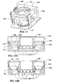
- FIG.s 14A and 14B depict alternate the exemplary embodiments of the invention including inserts 310, 312, 314 that fit within the channel 134.
- the inserts can be fastened with suitable fasteners (not shown).
- the insert 310 has a generally vertical wall 310a and a wall portion 310b that forms a part of a cone.
- the channel shape is modified by the use of two inserts 312, 314.
- the insert 314 changes the shape of the inner wall 134c to adjust the radiation reflecting characteristics of that wall 134c.
- the second insert 312 modifies the slope of the wall 134d as well as modifying the generally vertical outer wall 134b.
- Walls of the insert facing the radiant energy emitting bulbs are finished or coated with a gold coating as are the other reflecting surfaces to provide efficient reflection of the radiant energy off those surfaces.
- the radiant energy reflecting characteristics of the source 110 are modified in a controlled fashion based on a new walls geometry or shape for the channel 132 ( FIG. 2 ). The purpose of this arrangement is to provide a cost effective and efficient way to reuse an array of initial reflector configuration for a different process application or different tool.
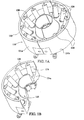
- FIG.s 15 and 16 illustrate an alternate embodiment of the invention wherein the reflecting walls 134c, 134d that form inner and outer walls of the channel 132 are defined by inscribed polyhedron surfaces with a number of faces or facets equal to a number of heating elements in the array of heating.
- the embodiment of FIG.s 15 and 16 may be preferably for use in making the fabrication of the source more economic.
- FIG. 17A - 17C illustrate alternate use of the invention.
- a base 330 is depicted in FIG. 17C .
- This base 330 has a top surface 332 which supports either of the two channel defining members 334, 336 shown in FIG.s 17A and 17B respectively.
- the channel defining member 334 has a substantially vertical outer wall 350 that meets a cone shaped outer wall 352.
- An inner wall 354 is also cone shaped and defines a sloped inner boundary for the channel which accommodates the multiple heating sources spaced within the circumference of the channel.
- a vertical segment 360 of the channel boundary is shorter than the vertical outer wall 350 of FIG.
- each of the two channel defining members 334, 336 has its own radiant energy reflecting characteristics and is selectively chosen for different process application or tools and attached to the base 330, for example, by means of suitable fasteners.
- the base is reused and process modification simplified with such arrangement.
- FIG. 18 illustrates use of a outer wall portion 370 of the source reflector at least a part of which is made of curved surface of revolution. It may in section define a part of ellipse or parabola or circle or any other curve.
- the reflecting surfaces of the source also includes portions that are straight lines that revolved around a center axis to form a cylinder or cone or horizontal surface. This curved line in FIG. 18 is convex facing a direction of the bulbs.
- prior art for example household and others radiant heaters use a parabola or ellipse or similar shapes, that are concave facing a bulb and therefore concentrate the light to a particular region.
- Use of a convex shape such as the shape in FIG. 18 , will spread the individual element energy from a given bulb over a larger area, making total, superposed from all elements heat distribution smoother and more uniform.
Landscapes
- Resistance Heating (AREA)
- Control Of Resistance Heating (AREA)
Claims (20)
- Strahlungsquelle (110) zum Erhitzen eines relativ zu der Strahlungsquelle positionierten Werkstücks (112), umfassend:mehrere Strahlungsheizelemente (120), die im Allgemeinen konzentrisch um eine Quellenmittelachse angeordnet sind; undeinen Reflektor mit einer reflektierenden Oberfläche, die einen einzigen Kanal (132) begrenzt, der sich in einer Richtung eines Werkstücks (112) öffnet und die Heizelemente (120) enthält, wobei der Reflektor eine innere Wand (134c), äußere Wände (134b, d) und eine Bodenwand umfasst, die sich um mindestens einen Abschnitt der Mittelachse (122) herum erstrecken, um den einzigen Kanal zu definieren, und die zum Reflektieren von durch die Heizelemente (120) abgestrahlter Strahlungsenergie zu einem durch das Werkstück (112) belegten Bereich oberflächenendbearbeitet sind;wobei die Bodenwand des einzigen Kanals einen Teil einer ebenen Rotationsoberfläche und die innere Wand und die äußeren Wände einen Teil einer konischen Rotationsoberfläche umfassen, welche zwei oder mehrere benachbarte Heizelemente (120) umspannen, derart, dass sich der einzige Kanal nach außen zu dem Werkstück (112) hin aufweitet, um Strahlungsenergie zu dem Werkstück (112) hin zu reflektieren; dadurch gekennzeichnet, dass die mehreren Strahlungsheizelemente (120) in einem einzigen Array angeordnet sind; und die Heizelemente jeweils eine Mittelachse umfassen, die in Bezug auf eine Mittelachse des einzigen Arrays in einem Winkel ausgerichtet ist.
- Strahlungsquelle (110) nach Anspruch 1, wobei einige oder alle der reflektierenden Oberflächen aus einem Quellensockel (130), der die Strahlungsheizelemente (120) trägt, gebildet sind.
- Strahlungsquelle nach Anspruch 1, wobei mindestens ein Abschnitt des einzigen Kanals (132) durch eine Wand begrenzt ist, die eine reflektierende Oberfläche aufweist, welche in einem Querschnitt in einem rechten Winkel zu einer Quellenmittelachse (122) eine einbeschriebene Polyederoberfläche umfasst, wobei die Anzahl von Seiten mindestens gleich der Anzahl von Heizelementen in dem einzeigen Array aus Heizelementen (120) ist.
- Strahlungsquelle nach Anspruch 1, wobei die reflektierende Oberfläche aus Teilen des Reflektors gebildet ist, welche innere, äußere und/oder untere Rotationsoberflächen um die Heizquellenmittelachse definieren, die mit ihren Achsen mit der Quellenmittelachse ausgerichtet montiert oder angebracht sind.
- Strahlungsquelle (110) nach Anspruch 1, umfassend unterschiedliche Sätze der koaxialen Reflektoren von unterschiedlicher Gestalt und einen einzigen Reflektorsockel, um zu ermöglichten, unterschiedliche Reflektorensätze an einem gemeinsamen Sockel anzubringen.
- Strahlungsquelle (110) nach Anspruch 1, die derart betrieben werden kann, dass sie zusätzliche austauschbare reflektierende Einsätze (310, 312, 314) umfasst, welche ebene und/oder zylinderförmige und/oder konische und/oder konvex gekrümmte Rotationsoberflächen umfassen, die koaxial in dem Reflektor angeordnet werden, um einen Teil der Strahlungsenergie in (einer) anderen Richtung(en) umzuverteilen.
- Strahlungsquelle (110) nach Anspruch 1, welche eine Wand (134b) umfasst, die einen Lippenabschnitt (134e) aufweist, der über einen Abschnitt des einzigen Kanals (132) vorragt, um Energie zu den anderen Reflektoroberflächen, welche den Kanal (132) begrenzen, zurück zu reflektieren, um Strahlungsenergie, die, wäre kein Lippenabschnitt (134e) vorhanden, das Ziel verfehlen würde, abzufangen und zu dem Werkstück zurück umzuleiten.
- Strahlungsquelle nach Anspruch 1, welche eine Positionierung der Heizelemente (120) relativ zu dem Reflektor vorsieht, die von elektrischen Anschlüssen, welche die Strahlungsheizelemente mit Energie versorgen, mechanisch unabhängig ist.
- Strahlungsquelle (110) nach Anspruch 1, wobei die Heizelemente (120) einzelne längliche Kolben (138) umfassen, die in Bezug auf die Mittelachse (122) des Array oder Werkstücks in einem Winkel angeordnet sind.
- Strahlungsquelle (110) nach Anspruch 9, welche eine Zwischenbuchse (150) zum Lagern der Heizelemente (120) relativ zu dem Reflektor einbindet, wobei die Buchsen (150) ein hochgradig thermisch leitfähiges Material umfassen.
- Strahlungsquelle (110) nach Anspruch 9, wobei der Reflektor einen Reflektorsockel umfasst, der eine Anzahl von Durchgängen (135) zum Ausrichten der Heizelemente (120) in dem Kanal umfasst.
- Strahlungsquelle (110) nach Anspruch 11, wobei die Buchsen (150) die Ausrichtung der Heizelemente (120) festlegen und in den Reflektorsockel-Durchgängen (135) positioniert sind.
- Verfahren zur Verwendung beim Erhitzen eines Werkstücks (112), umfassend:Bereitstellen eines Strahlungswärmereflektors mit einer reflektierenden Oberfläche, die einen einzigen Kanal (132) bildet, der sich um mindestens einen Abschnitt einer Mittelachse (122) herum erstreckt, wobei die reflektierende Oberfläche eine innere Wand und äußere Wände (134c; 134b, d) umfasst, welche einen Teil einer zylinderförmigen und/oder konischen und/oder konvex gekrümmten Rotationsoberfläche bilden, die sich nach außen zu einem Werkstückbereich hin aufweitet;Anbringen mehrerer Strahlungsheizelemente (120) in dem einzigen Kanal (132) des Reflektors in einem Array, welches im Allgemeinen konzentrisch um die Mittelachse (122) angeordnet ist, derart, dass die Wände des einzigen Kanals (132) zwei oder mehr benachbarte Heizelemente (120) umspannen, um Strahlungsenergie zu einem Werkstückbereich hin zu reflektieren, derart, dass die Strahlungsheizelemente in Bezug auf eine Mittelachse des einzigen Array in einem Winkel angeordnet sind; undregelbares Einschalten der Heizelemente (120), um Strahlungsenergie von den Heizelementen abzustrahlen, zum Richten von Strahlungsenergie zu dem Werkstückbereich hin.
- Verfahren nach Anspruch 13, ferner umfassend das Endbearbeiten der reflektierenden Oberfläche mit einer strahlungsenergiereflektierenden Beschichtung, um Strahlungsenergie, die durch die Heizelemente (120) zu dem Werkstückbereich hin abgestrahlt wird, zu reflektieren.
- Verfahren nach Anspruch 13, wobei einige oder alle der reflektierenden Oberflächen des einzigen Kanals (132) aus einem Quellensockel (130), der die Strahlungsheizelemente (120) trägt, gebildet sind.
- Verfahren nach Anspruch 15, wobei der Schritt des Anbringens des Heizelements (120) durch Koppeln der Heizelemente (120) mit einer Zwischenbuchse (150) und Befestigen der Buchse an dem Quellensockel (130) durchgeführt wird.
- Verfahren nach Anspruch 16, ferner umfassend den Schritt des Befestigens eines Heizelementeinschaltkreises an elektrischen Kontakten, deren Position durch die Buchse (150) festgelegt wird.
- Verfahren nach Anspruch 15, umfassend das Einführen unterschiedlicher Sätze der koaxialen Reflektoren von unterschiedlicher Gestalt in den Kanal (132), der durch den Quellensockel (130) definiert wird, um zu ermöglichen, unterschiedliche Reflektorensätze an einem gemeinsamen Sockel anzubringen.
- Verfahren nach Anspruch 15, ferner umfassend das Einführen von austauschbaren reflektierenden Einsätzen (310, 312, 314) mit ebenen und/oder zylinderförmigen und/oder konischen und/oder gekrümmten konvexen Rotationsoberflächen, die koaxial in dem Wärmereflektor angeordnet werden, um einen Teil der Strahlungsenergie in (eine) andere Richtung(en) umzuverteilen.
- Verfahren nach Anspruch 13, umfassend das Umverteilen von Energie durch Abfangen von Energie von den Heizelementen mit einem Lippenabschnitt (134e), welcher über einen Abschnitt des Kanals (132) vorragt, um Energie zu anderen Reflektoroberflächen, die den Kanal begrenzen, zurück zu reflektieren.
Applications Claiming Priority (3)
| Application Number | Priority Date | Filing Date | Title |
|---|---|---|---|
| US361658 | 1982-03-25 | ||
| US10/361,658 US6947665B2 (en) | 2003-02-10 | 2003-02-10 | Radiant heating source with reflective cavity spanning at least two heating elements |
| PCT/US2004/004160 WO2004073050A1 (en) | 2003-02-10 | 2004-02-10 | Radiant heating source |
Publications (2)
| Publication Number | Publication Date |
|---|---|
| EP1593146A1 EP1593146A1 (de) | 2005-11-09 |
| EP1593146B1 true EP1593146B1 (de) | 2010-06-09 |
Family
ID=32824277
Family Applications (1)
| Application Number | Title | Priority Date | Filing Date |
|---|---|---|---|
| EP04709941A Expired - Lifetime EP1593146B1 (de) | 2003-02-10 | 2004-02-10 | Strahlungs-wärme-quelle |
Country Status (8)
| Country | Link |
|---|---|
| US (1) | US6947665B2 (de) |
| EP (1) | EP1593146B1 (de) |
| JP (1) | JP4953123B2 (de) |
| KR (1) | KR101052126B1 (de) |
| CN (1) | CN100401464C (de) |
| DE (1) | DE602004027602D1 (de) |
| TW (1) | TWI325044B (de) |
| WO (1) | WO2004073050A1 (de) |
Families Citing this family (28)
| Publication number | Priority date | Publication date | Assignee | Title |
|---|---|---|---|---|
| KR101301797B1 (ko) * | 2004-02-05 | 2013-08-29 | 차이나 파워 테크날러지 리미티드 | 라디에이터 장치 |
| KR100621777B1 (ko) * | 2005-05-04 | 2006-09-15 | 삼성전자주식회사 | 기판 열처리 장치 |
| JP2008182180A (ja) * | 2006-12-26 | 2008-08-07 | Epicrew Inc | 加熱装置及び半導体製造装置 |
| JP5104405B2 (ja) * | 2008-03-03 | 2012-12-19 | 株式会社デンソー | 半導体製造装置 |
| US8294068B2 (en) * | 2008-09-10 | 2012-10-23 | Applied Materials, Inc. | Rapid thermal processing lamphead with improved cooling |
| US7932665B2 (en) * | 2008-12-02 | 2011-04-26 | Osram Sylvania Inc. | Dual filament lamp for rapid temperature processing |
| US9027623B2 (en) * | 2009-09-22 | 2015-05-12 | Flexible Steel Lacing Company | Welding apparatus for conveyor belts and method |
| JP6038503B2 (ja) * | 2011-07-01 | 2016-12-07 | 株式会社日立国際電気 | 基板処理装置及び半導体装置の製造方法 |
| KR101911722B1 (ko) * | 2012-01-10 | 2018-10-25 | 에스케이실트론 주식회사 | 반도체 제조장치용 정렬 장치 |
| WO2013126324A1 (en) * | 2012-02-24 | 2013-08-29 | Applied Materials, Inc. | Heating lamp having base to facilitate reduced air flow about the heating lamp |
| ES2681370T3 (es) | 2012-12-28 | 2018-09-12 | Flexible Steel Lacing Company | Aparato y método de soldadura para cintas transportadoras |
| US10405375B2 (en) | 2013-03-11 | 2019-09-03 | Applied Materials, Inc. | Lamphead PCB with flexible standoffs |
| US9613835B2 (en) | 2013-03-15 | 2017-04-04 | Applied Materials, Inc. | Heating lamp assembly |
| US10410890B2 (en) * | 2013-06-21 | 2019-09-10 | Applied Materials, Inc. | Light pipe window structure for thermal chamber applications and processes |
| KR102347317B1 (ko) * | 2013-09-05 | 2022-01-06 | 어플라이드 머티어리얼스, 인코포레이티드 | 감소된 코일 가열을 위한 램프 단면 |
| CN107546157A (zh) * | 2013-11-22 | 2018-01-05 | 应用材料公司 | 易取灯头 |
| CN106133888B (zh) | 2013-12-19 | 2019-10-01 | 应用材料公司 | 用于可替换的灯的适配器 |
| US10763142B2 (en) | 2015-06-22 | 2020-09-01 | Lam Research Corporation | System and method for determining field non-uniformities of a wafer processing chamber using a wafer processing parameter |
| US10381248B2 (en) | 2015-06-22 | 2019-08-13 | Lam Research Corporation | Auto-correction of electrostatic chuck temperature non-uniformity |
| US10386821B2 (en) * | 2015-06-22 | 2019-08-20 | Lam Research Corporation | Systems and methods for calibrating scalar field contribution values for a limited number of sensors including a temperature value of an electrostatic chuck and estimating temperature distribution profiles based on calibrated values |
| US10932323B2 (en) | 2015-08-03 | 2021-02-23 | Alta Devices, Inc. | Reflector and susceptor assembly for chemical vapor deposition reactor |
| DE102015115628A1 (de) * | 2015-09-16 | 2017-03-16 | Rainer Förster | Infrarotheizung |
| US12040200B2 (en) | 2017-06-20 | 2024-07-16 | Asm Ip Holding B.V. | Semiconductor processing apparatus and methods for calibrating a semiconductor processing apparatus |
| KR102232654B1 (ko) * | 2019-08-05 | 2021-03-26 | 주식회사 에이치에스하이테크 | 엘이디 스핀척 |
| WO2022261988A1 (zh) * | 2021-06-18 | 2022-12-22 | 深圳汝原科技有限公司 | 辐射源组件和干燥设备 |
| KR102514718B1 (ko) * | 2021-09-09 | 2023-03-27 | 백승원 | 하이브리드 가열시스템을 갖는 열처리용 전기로 |
| CN116216301B (zh) * | 2023-05-06 | 2023-07-04 | 成都德力斯实业有限公司 | 一种放射性无菌注射剂生产线 |
| CN119243123B (zh) * | 2023-07-03 | 2026-02-06 | 北京北方华创微电子装备有限公司 | 一种加热装置及半导体处理设备 |
Family Cites Families (23)
| Publication number | Priority date | Publication date | Assignee | Title |
|---|---|---|---|---|
| DE383360C (de) * | 1923-10-12 | Wiskot Licht Ges M B H | Strahlungsheizkoerper mit Hohlspiegelreflektor | |
| US1231750A (en) * | 1915-09-09 | 1917-07-03 | American Electrical Heater Co | Luminous electric heater. |
| US3761678A (en) * | 1971-05-03 | 1973-09-25 | Aerojet General Co | High density spherical modules |
| JPS59169125A (ja) * | 1983-03-16 | 1984-09-25 | Ushio Inc | 半導体ウエハ−の加熱方法 |
| US4716658A (en) * | 1986-12-11 | 1988-01-05 | Amjo Infra Red Dryers, Inc. | Heat lamp assembly |
| US4891499A (en) * | 1988-09-09 | 1990-01-02 | Texas Instruments Incorporated | Method and apparatus for real-time wafer temperature uniformity control and slip-free heating in lamp heated single-wafer rapid thermal processing systems |
| DE4001280A1 (de) * | 1990-01-18 | 1991-07-25 | Meyer Kobbe Clemens | Vorrichtung zur oberflaechenbehandlung von werkstuecken mittels lichtstrahlen |
| US5155336A (en) | 1990-01-19 | 1992-10-13 | Applied Materials, Inc. | Rapid thermal heating apparatus and method |
| US5446825A (en) * | 1991-04-24 | 1995-08-29 | Texas Instruments Incorporated | High performance multi-zone illuminator module for semiconductor wafer processing |
| US5418885A (en) * | 1992-12-29 | 1995-05-23 | North Carolina State University | Three-zone rapid thermal processing system utilizing wafer edge heating means |
| US5345534A (en) * | 1993-03-29 | 1994-09-06 | Texas Instruments Incorporated | Semiconductor wafer heater with infrared lamp module with light blocking means |
| US5740314A (en) | 1995-08-25 | 1998-04-14 | Edison Welding Institute | IR heating lamp array with reflectors modified by removal of segments thereof |
| JP3996663B2 (ja) * | 1996-02-28 | 2007-10-24 | 東京エレクトロン株式会社 | ランプ加熱型熱処理装置 |
| TW315493B (en) * | 1996-02-28 | 1997-09-11 | Tokyo Electron Co Ltd | Heating apparatus and heat treatment apparatus |
| JPH09237763A (ja) * | 1996-02-28 | 1997-09-09 | Tokyo Electron Ltd | 枚葉式の熱処理装置 |
| US6023555A (en) | 1998-08-17 | 2000-02-08 | Eaton Corporation | Radiant heating apparatus and method |
| US6210484B1 (en) * | 1998-09-09 | 2001-04-03 | Steag Rtp Systems, Inc. | Heating device containing a multi-lamp cone for heating semiconductor wafers |
| US6122440A (en) * | 1999-01-27 | 2000-09-19 | Regents Of The University Of Minnesota | Optical heating device for rapid thermal processing (RTP) system |
| US6259072B1 (en) | 1999-11-09 | 2001-07-10 | Axcelis Technologies, Inc. | Zone controlled radiant heating system utilizing focused reflector |
| JP3659863B2 (ja) * | 2000-04-06 | 2005-06-15 | 大日本スクリーン製造株式会社 | 熱処理装置 |
| JP4058231B2 (ja) * | 2000-11-13 | 2008-03-05 | 株式会社東芝 | 半導体装置の製造方法 |
| CN1373497A (zh) * | 2001-02-28 | 2002-10-09 | 世罗技术株式会社 | 带卤素灯的辐射加热器 |
| AUPR548801A0 (en) * | 2001-06-06 | 2001-06-28 | Alver Pty. Ltd. | Room conditioning |
-
2003
- 2003-02-10 US US10/361,658 patent/US6947665B2/en not_active Expired - Lifetime
-
2004
- 2004-02-10 DE DE602004027602T patent/DE602004027602D1/de not_active Expired - Lifetime
- 2004-02-10 KR KR1020057014712A patent/KR101052126B1/ko not_active Expired - Fee Related
- 2004-02-10 EP EP04709941A patent/EP1593146B1/de not_active Expired - Lifetime
- 2004-02-10 TW TW093103010A patent/TWI325044B/zh not_active IP Right Cessation
- 2004-02-10 JP JP2006503530A patent/JP4953123B2/ja not_active Expired - Fee Related
- 2004-02-10 CN CNB2004800094408A patent/CN100401464C/zh not_active Expired - Fee Related
- 2004-02-10 WO PCT/US2004/004160 patent/WO2004073050A1/en not_active Ceased
Also Published As
| Publication number | Publication date |
|---|---|
| CN100401464C (zh) | 2008-07-09 |
| DE602004027602D1 (de) | 2010-07-22 |
| EP1593146A1 (de) | 2005-11-09 |
| TW200504323A (en) | 2005-02-01 |
| CN1771582A (zh) | 2006-05-10 |
| JP4953123B2 (ja) | 2012-06-13 |
| US6947665B2 (en) | 2005-09-20 |
| WO2004073050A1 (en) | 2004-08-26 |
| KR20050094482A (ko) | 2005-09-27 |
| KR101052126B1 (ko) | 2011-07-26 |
| TWI325044B (en) | 2010-05-21 |
| US20040156625A1 (en) | 2004-08-12 |
| JP2006518552A (ja) | 2006-08-10 |
Similar Documents
| Publication | Publication Date | Title |
|---|---|---|
| US6947665B2 (en) | Radiant heating source with reflective cavity spanning at least two heating elements | |
| KR100729006B1 (ko) | 열 처리 챔버들에서 반도체 웨이퍼들을 가열하기 위한 가열 디바이스 | |
| US4789771A (en) | Method and apparatus for substrate heating in an axially symmetric epitaxial deposition apparatus | |
| KR100217486B1 (ko) | 반도체 공정에서 기판을 가열하기 위한 장치 및 방법 | |
| JP4911819B2 (ja) | 二表面反射体 | |
| US6570134B2 (en) | Heat treatment device of the light irradiation type and heat treatment process of the irradiation type | |
| JPS6293378A (ja) | 軸対称的なエピタキシヤル成長装置中で基板を加熱するための方法及び装置 | |
| JP4141441B2 (ja) | 急速熱処理装置の加熱モジュール | |
| KR20150004360A (ko) | 원뿔형 석영 돔을 통해 투과되는 광을 제어하기 위한 광학계 | |
| TW202245105A (zh) | 一種反射板組、燈組模組、襯底處理設備及反射板組的調節方法 | |
| US5889258A (en) | High temperature heating apparatus | |
| CN105493231A (zh) | 圆形灯阵列 | |
| US7038173B2 (en) | Thermal processing apparatus and thermal processing method | |
| JP3504436B2 (ja) | 基板の枚葉式熱処理装置 | |
| US6023555A (en) | Radiant heating apparatus and method | |
| KR20240077647A (ko) | 에피택셜 공정용 반도체 제조 장치 | |
| JP2002075899A (ja) | 円形状平板試料の均熱装置 | |
| CN119560421A (zh) | 加热装置及工艺处理设备 | |
| CN118522673A (zh) | 加热装置及半导体工艺处理设备 | |
| KR20070019054A (ko) | 급속열처리설비의 가열장치 |
Legal Events
| Date | Code | Title | Description |
|---|---|---|---|
| PUAI | Public reference made under article 153(3) epc to a published international application that has entered the european phase |
Free format text: ORIGINAL CODE: 0009012 |
|
| 17P | Request for examination filed |
Effective date: 20050906 |
|
| AK | Designated contracting states |
Kind code of ref document: A1 Designated state(s): AT BE BG CH CY CZ DE DK EE ES FI FR GB GR HU IE IT LI LU MC NL PT RO SE SI SK TR |
|
| AX | Request for extension of the european patent |
Extension state: AL LT LV MK |
|
| DAX | Request for extension of the european patent (deleted) | ||
| RBV | Designated contracting states (corrected) |
Designated state(s): DE FR GB |
|
| 17Q | First examination report despatched |
Effective date: 20060425 |
|
| GRAP | Despatch of communication of intention to grant a patent |
Free format text: ORIGINAL CODE: EPIDOSNIGR1 |
|
| GRAS | Grant fee paid |
Free format text: ORIGINAL CODE: EPIDOSNIGR3 |
|
| GRAA | (expected) grant |
Free format text: ORIGINAL CODE: 0009210 |
|
| AK | Designated contracting states |
Kind code of ref document: B1 Designated state(s): DE FR GB |
|
| REF | Corresponds to: |
Ref document number: 602004027602 Country of ref document: DE Date of ref document: 20100722 Kind code of ref document: P |
|
| PLBE | No opposition filed within time limit |
Free format text: ORIGINAL CODE: 0009261 |
|
| STAA | Information on the status of an ep patent application or granted ep patent |
Free format text: STATUS: NO OPPOSITION FILED WITHIN TIME LIMIT |
|
| 26N | No opposition filed |
Effective date: 20110310 |
|
| PGFP | Annual fee paid to national office [announced via postgrant information from national office to epo] |
Ref country code: FR Payment date: 20110201 Year of fee payment: 8 Ref country code: DE Payment date: 20110228 Year of fee payment: 8 |
|
| REG | Reference to a national code |
Ref country code: DE Ref legal event code: R097 Ref document number: 602004027602 Country of ref document: DE Effective date: 20110309 |
|
| GBPC | Gb: european patent ceased through non-payment of renewal fee |
Effective date: 20110210 |
|
| PG25 | Lapsed in a contracting state [announced via postgrant information from national office to epo] |
Ref country code: GB Free format text: LAPSE BECAUSE OF NON-PAYMENT OF DUE FEES Effective date: 20110210 |
|
| REG | Reference to a national code |
Ref country code: FR Ref legal event code: ST Effective date: 20121031 |
|
| REG | Reference to a national code |
Ref country code: DE Ref legal event code: R119 Ref document number: 602004027602 Country of ref document: DE Effective date: 20120901 |
|
| PG25 | Lapsed in a contracting state [announced via postgrant information from national office to epo] |
Ref country code: FR Free format text: LAPSE BECAUSE OF NON-PAYMENT OF DUE FEES Effective date: 20120229 |
|
| PG25 | Lapsed in a contracting state [announced via postgrant information from national office to epo] |
Ref country code: DE Free format text: LAPSE BECAUSE OF NON-PAYMENT OF DUE FEES Effective date: 20120901 |