EP1590730B1 - Optoelektronische eingabeeinrichtung, verfahren zur herstellung einer solchen einrichtung und verfahren zur messung der bewegung eines objekts mit hilfe einer solchen einrichtung - Google Patents
Optoelektronische eingabeeinrichtung, verfahren zur herstellung einer solchen einrichtung und verfahren zur messung der bewegung eines objekts mit hilfe einer solchen einrichtung Download PDFInfo
- Publication number
- EP1590730B1 EP1590730B1 EP04704311A EP04704311A EP1590730B1 EP 1590730 B1 EP1590730 B1 EP 1590730B1 EP 04704311 A EP04704311 A EP 04704311A EP 04704311 A EP04704311 A EP 04704311A EP 1590730 B1 EP1590730 B1 EP 1590730B1
- Authority
- EP
- European Patent Office
- Prior art keywords
- laser
- mounting board
- radiation
- measuring
- cavity
- Prior art date
- Legal status (The legal status is an assumption and is not a legal conclusion. Google has not performed a legal analysis and makes no representation as to the accuracy of the status listed.)
- Expired - Lifetime
Links
Images
Classifications
-
- G—PHYSICS
- G06—COMPUTING OR CALCULATING; COUNTING
- G06F—ELECTRIC DIGITAL DATA PROCESSING
- G06F3/00—Input arrangements for transferring data to be processed into a form capable of being handled by the computer; Output arrangements for transferring data from processing unit to output unit, e.g. interface arrangements
- G06F3/01—Input arrangements or combined input and output arrangements for interaction between user and computer
- G06F3/03—Arrangements for converting the position or the displacement of a member into a coded form
- G06F3/041—Digitisers, e.g. for touch screens or touch pads, characterised by the transducing means
- G06F3/042—Digitisers, e.g. for touch screens or touch pads, characterised by the transducing means by opto-electronic means
- G06F3/0421—Digitisers, e.g. for touch screens or touch pads, characterised by the transducing means by opto-electronic means by interrupting or reflecting a light beam, e.g. optical touch-screen
-
- G—PHYSICS
- G06—COMPUTING OR CALCULATING; COUNTING
- G06F—ELECTRIC DIGITAL DATA PROCESSING
- G06F3/00—Input arrangements for transferring data to be processed into a form capable of being handled by the computer; Output arrangements for transferring data from processing unit to output unit, e.g. interface arrangements
- G06F3/01—Input arrangements or combined input and output arrangements for interaction between user and computer
- G06F3/03—Arrangements for converting the position or the displacement of a member into a coded form
-
- G—PHYSICS
- G06—COMPUTING OR CALCULATING; COUNTING
- G06F—ELECTRIC DIGITAL DATA PROCESSING
- G06F3/00—Input arrangements for transferring data to be processed into a form capable of being handled by the computer; Output arrangements for transferring data from processing unit to output unit, e.g. interface arrangements
Definitions
- the invention relates to an optoelectronic input device in which the input is formed by detected movements of an object, the device comprising an optical module comprising at least one laser with a cavity for the generation of a measuring radiation beam, optical means for the guidance of the radiation beam to a plane close to the object and converting means for the conversion of radiation of the measuring radiation beam reflected and modulated by the object into an electrical signal, the converting means being formed by the combination of the cavity of the laser and measuring means for the measuring of a change in the cavity during operation, which is caused by the reflected radiation entering the cavity, which radiation is representative of a movement of the object relative to the module, the optical module comprising a laser which is mounted on a mounting board with its cavity parallel thereto, and the optical means comprising an optical component mounted on the mounting board and aligned to the laser from where the measuring radiation beam emitted by the laser goes to the plane close to the object via a further optical component which is at least partly transparent and of which the upper side forms the plane close to the object.
- a device of this kind is particularly suitable as input means for a PC, where the function of the document so-called mouse can then be taken over.
- the device is even more suitable as a scroll and click device in a portable unit, such as a mobile telephone, for the operation of a so-called scrolling menu.
- movements of the input and output medium can be detected with the device.
- the invention also relates to a method of operation for the production of such a device and a method of operation for measuring the movement of an object with the help of such a device.
- FIG. 9a an input device is shown where, on a mounting board, which is formed as a foot fitted with mounting pins, a laser is mounted with its cavity parallel to the mounting board.
- the device comprises three such lasers which are assembled at 120-degree angles (see Fig. 9b).
- the cavity forms, together with measuring means, converting means for the reflected radiation, a change occurring in the cavity being representative of a relative movement of the object.
- the measuring means could for example comprise means for the measurement of a change in the impedance of the laser cavity. Also a radiation detector is suitable for this purpose.
- EP 0.810.589 discloses an optical pick-up device with a plurality of laser couplers.
- the radiation beam emitted by a laser is reflected on a block and the reflected part of the beam goes via a lens to a working plane formed by an optical disk. A part of the radiation enters the block and is used for focusing purposes.
- a disadvantage of the known device is that it is not sufficiently compact for many applications for which ever smaller dimensions are being demanded. Above all, large scale production of the device is not easy and not inexpensive.
- the further optical component includes a block-shaped body which is surface mounted next to the laser directly on to the mounting board and which, when viewed in projection, has no overlap with the laser, and of which at least the uppermost part is optically transparent.
- the device can be relatively compact.
- the measuring radiation beam can be led to the block-shaped body at a small angle to the mounting board. With this small angle the radiation beam can reflect within the transparent part of the block-shaped body backwards and forwards a number of times before the upper plane is reached.
- both the lateral dimensions and the height of the device are limited, while yet a relatively large optical range is created for the radiation beam as required for proper operation of the device.
- the most important components of the device such as the laser, the optical component, which for example comprises a mirror, and the block-shaped body, can now be attached to the mounting board all by means of surface mounting. This can be done with relatively high precision of alignment, and fast and cheaply, with the help of so-called pick and place machines.
- the block-shaped body does not in any way have any overlap particularly with the laser, it can easily be enclosed by a transparent plastic material.
- a liquid transparent plastic material which cures after application is particularly suited for this purpose.
- one side of a first part of the transparent uppermost part of the block-shaped body directed towards the measuring radiation beam is made tilted outwards. This enables any interruption of the measuring radiation beam on entering the block-shaped body to be corrected.
- the angle of said side to the normal would amount for example to 30 degrees.
- the uppermost part of the block-shaped body further includes a second part lying on the first part, with its side planes approximately vertical to the mounting board. Within this part the radiation beam can reflect a number of times.
- the measuring means comprise a radiation detector mounted on the mounting board and the optical component comprises a converging mirror which is located on a side plane of a further block-shaped body which is mounted on the mounting board, and this side plane is fitted with a further mirror which casts part of the radiation emitted by the laser on the radiation detector.
- the laser, the measuring means and the optical means are enveloped in a cured optically transparent gel which also includes the whole radiation path from the laser to the block shaped body.
- a cured optically transparent gel which also includes the whole radiation path from the laser to the block shaped body.
- the mounting board is in an electrically and thermally insulated material and one side of the mounting board is fitted with a conductor unit to which the laser and the measuring means are connected.
- a conductor unit to which the laser and the measuring means are connected.
- the device is above all inexpensive, because a large number of devices can be produced at the same time.
- the mounting board has an opening near the laser of which opening at least the walls are covered with a thermally conductive material which forms a heatsink for the laser or which forms a thermal connection between the laser and a heatsink for the laser. If the opening is completely filled with a material such as copper the laser can be mounted on it. If so desired the laser can advantageously also be mounted next to the opening, and in this way the conductive material in the opening connects the laser with a heatsink fitted under the mounting board.
- a method of operation for the measurement of the movement of an object in relation to an input device is characterized according to the invention by the fact that use is made of an optoelectronic input device in accordance with one of the above-mentioned conclusions. Because of the compactness the device is particularly suitable for application as input unit for operating a so-called scroll menu in the operation of a mobile telephone. Also, in a laptop computer, the device can advantageously be applied as a so-called pressure cushion for finger operation of various menus.
- a method of operation for the production of an optoelectronic input device in which the input is formed by detected movements of an object and the device comprises an optical module containing at least one laser with a cavity for the generation of a measuring radiation beam, optical means for leading the radiation beam to a plane close to the object and converting means for converting the radiation of the measuring radiation beam reflected by the object into an electrical signal, in which the converting means are formed by the combination of the cavity of the laser and measuring means for the measurement of a change in the cavity during operation which is caused by interference of the reflected beam of the measuring radiation beam which penetrates into the cavity and the constant wave in the cavity and which is representative of a relative movement of the object in relation to the module, the optical module being formed by a mounting board on which a laser is mounted with its cavity parallel to this board and the optical means comprising an optical component mounted on the mounting board and aligned to the laser for the measuring radiation beam emitted by the laser which is led from there to the plane close to the object via a further optical component which is at least partly transparent and
- the measuring means are formed by a radiation detector which is mounted on the mounting board and the optical component is formed as a converging mirror and attached to a side plane of a further block-shaped body which is mounted on the mounting board, and which side plane is fitted with a further mirror which casts part of the radiation emitted by the laser on the radiation detector.
- the laser, the measuring means and the optical means are covered with a liquid optically transparent gel which envelopes the whole radiation path from the laser to the block-shaped body and which cures after application.
- an electrically and thermally insulating material is chosen for the material of the mounting board of which one side is fitted with a conductor unit to which the laser and the measuring means are connected.
- the most important parts are attached to the mounting board by means of surface mounting.
- the parts of the device such as the laser, the further optical component, the optical means and the measuring means can be placed on the mounting board with the help of standard pick and place machines.
- the parts that do not need any electrical connection such as the block-shaped body and the further block-shaped body can be advantageously attached and aligned in this way.
- the underside of these parts will be specially provided with a metal layer.
- a laser and detector crystal will have a conductive layer of this kind as standard.
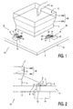
- the input device 10 shown in Fig. 1 comprises a module 11 with a mounting board 4, here a PCB 4. On this board there is a conductor unit 9', here in the form of copper regions 9. On them a laser 1 and a photodiode 3 are mounted. For the top connection of the laser 1 and the photodiode 3 use is made of a wire connection 20. On one side of the laser 1 and the photodiode 3 are located optical means 2 in the form of a converging mirror 2 which receives a measuring radiation beam S emitted by the laser 1 - here an angle of approximately 30 degrees to the mounting board - and guides this to a further optical component (see Fig.
- the module 11 contains more lasers 1,1' of which only two are to be seen in the drawing. Also the parts 2,3 associated with each laser 1, 1' are present in corresponding numbers.
- the block-shaped body 5 is here completely made of a transparent plastic material, here PMMA.
- the radiation beam S enters (see Fig. 2 ) the body 5 via a first part 5A1 of the uppermost part 5A and reaches, after a number of reflections inside a part 5A2 lying on the first part 5A1, the top plane V of the body 5 over which (see Fig. 1 ) there is a moving object M, for example a piece of paper or, as shown in the Figure, the finger M of a person who is operating the device 10. Radiation reflected by the moving finger M travels the reverse way and reaches the cavity of the laser 1 and there causes a change as a result of the occurrence of interference caused by the movement of the finger.
- a moving object M for example a piece of paper or, as shown in the Figure, the finger M of a person who is operating the device 10.
- the occurrence of the change in the cavity of the laser 1 is measured with the help of a radiation detector 3, here a photodiode 3, on which part of the radiation emitted by the laser 1 is incident.
- a radiation detector 3 here a photodiode 3
- the mirror 2 which reflects the radiation beam S to the body 5 is mounted on the same side plane.
- the cavity, the further mirror 7 and the radiation detector 3 form converting means which convert the radiation reflected and modulated by the object M into an electrical signal. Further particulars of the detection of a finger movement are shown in patent application US 2002/0104957 referred to above.
- FIG. 2 there is an opening 12 in the mounting board 4 close to the laser 1, of which opening at least the walls are covered with a thermally conductive material 13, copper in this case, which connects the laser 1 with a heatsink 14 which is located on the side of the mounting board 4 opposite the laser 1.
- Each side plane of the first part SA1 of the uppermost part 5A of the block-shaped body 5 and located opposite a mirror 2-30 degrees to the normal here - is constructed tilted outwards. In this way any occurrence of reflection from the radiation beam S on entering the body 5 can be counteracted.
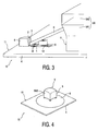
- Fig. 4 shows in a diagrammatic and perspective view an important variant of the device of Fig. 1 .
- a transparent plastic envelope 8 can be seen, which can be easily applied thanks to the absence of overlap between the body 5 and the further parts 3,6.
- the envelope 8 comprises the whole radiation path of the beam S between the laser and the body 5 and protects the parts covered thereby and contributes to a stable operation of the device 10, also because disturbing reflections are avoided or at least limited as a result thereof.
- a thin further envelope - not shown in the drawing - can be applied over the envelope 8 and which is not transparent to radiation.
- the envelope 8 is here a silicon-based plastic material, a material that is particularly suitable for this purpose.
- the upper plane V of the body 5 is embodied with an arched shape.
- the device according to the invention for example the embodiment 10 shown in the Figures, can be produced as follows with the help of a method of operation according to the invention.
- the starting point (see for example Fig. 1 ) is a PCB 4 which has an opening 12 of which the walls are covered with a copper layer 13.
- a conductor unit 9 is fitted for connection of electrically active parts such as the laser 1 and the photodiode 3.
- the alignment-sensitive parts such as the laser 1 and the photodiode 3
- the block-shaped body 5,6 solder regions - not visible in the drawing - are applied on the upper side of the plate 4 on previously determined and precise positions.
- the dimensions of these regions are chosen to be practically identical to the dimensions of the parts to be placed, such as laser 1, photodiode 3 and the bodies 5,6. All these parts 1,3,5 6 have on their underside a metal layer - not shown in the drawing either.
- an envelope in the form of drop 8 of a silicon plastic material is applied which covers the laser 1, the photodiode 3 and the mirror 2.
- the radiation path of the beam S between the laser and the body 5 is then found within this drop.
- the electrical connections of the electrically active parts 1,3 extend to outside the envelope 8 or are located if desired on the underside of the plate 4.
- the device 10 is ready for use. Thanks to the construction of the module 11 a large number of devices 10 can easily be produced at the same time. They can be separated from one another by a separation technique such as sawing.
- the dimensions of an individual device 10 are approximately 30 x 30 mm, whereas the height is not more than 10 mm.
- the body 5 is 10 mm high and measures for example 5 mm x 5mm.
- the invention is not limited to the example of embodiment described since to a specialist many variations and modifications are possible within the framework of the invention.
- devices can be produced with a different geometry and/or different dimensions.
- the device according to the invention can also include one or more than two laser(s) and their associated parts.
- another substrate such as glass or ceramic substrate, may be used.
- the device may include further active and passive semiconductor elements or electronic components such as diodes and/or transistors and resistances and/or capacitances, whether or not in the form of an integrated circuit.
- the production is then obviously very much adapted to the purpose.
- a processor or other electronic equipment for the reading and/or control of the laser is included in this.
- a change in the cavity of a laser which change represents a finger movement, is established also in an exclusively electrical manner, for example by the measuring of the impedance of the cavity, as described in United States patent application US 2002/0104957 . Also the addition of a processor or other electronic components for reading and/or control of the laser is included in this.
Landscapes
- Engineering & Computer Science (AREA)
- Theoretical Computer Science (AREA)
- General Engineering & Computer Science (AREA)
- Human Computer Interaction (AREA)
- Physics & Mathematics (AREA)
- General Physics & Mathematics (AREA)
- Length Measuring Devices By Optical Means (AREA)
- Photometry And Measurement Of Optical Pulse Characteristics (AREA)
- Semiconductor Lasers (AREA)
- Optical Radar Systems And Details Thereof (AREA)
- Analysing Materials By The Use Of Radiation (AREA)
- Containers And Plastic Fillers For Packaging (AREA)
- Solid State Image Pick-Up Elements (AREA)
- Measurement Of Optical Distance (AREA)
Claims (16)
- Optoelektronische Eingabeeinrichtung (10), bei der die Eingabe durch detektierte Bewegungen eines Objekts (M) gebildet wird, wobei die Einrichtung ein optisches Modul (11) umfasst, das zumindest einen Laser (1,1') mit einem Hohlraum für die Erzeugung eines Messstrahlungsbündels (S), optische Mittel (2) für die Führung des Strahlungsbündels (S) zu einer Fläche (V) dicht bei dem Objekt (M) und Umwandlungsmittel für die Umwandlung von von dem Objekt (M) reflektierter und modulierter Strahlung des Messstrahlungsbündels (S) in ein elektrisches Signal umfasst, wobei die Umwandlungsmittel durch die Kombination des Hohlraums des Lasers (1) und Messmitteln (3) für die Messung einer durch die in den Hohlraum eintretende, reflektierte Strahlung bewirkten Änderung in dem Hohlraum beim Betrieb gebildet werden, welche Strahlung für eine Bewegung des Objektes (M) relativ zu dem Modul (11) repräsentativ ist, wobei das optische Modul (11) den Laser (1) umfasst, der auf einer Trägerplatte (4) montiert ist, mit seinem Hohlraum parallel dazu, und die optischen Mittel (2) ein auf der Trägerplatte (4) montiertes und zu dem Laser (1) ausgerichtetes optisches Bauelement (2) umfassen, von wo aus das von dem Laser (1) ausgesendete Messbündel (S) zu der Fläche (V) dicht bei dem Objekt (M) über ein weiteres optisches Bauelement verläuft, das zumindest teilweise transparent ist und dessen obere Seite die Fläche (V) dicht bei dem Objekt (M) bildet, dadurch gekennzeichnet, dass das weitere optische Bauelement einen blockförmigen Körper (5) enthält, der nahe dem Laser (1) direkt auf die Trägerplatte (4) oberflächenmontiert ist und der, in Projektion gesehen, keine Überlappung mit dem Laser (1) aufweist und von dem zumindest der oberste Teil (5A) optisch transparent ist.
- Optoelektronische Eingabeeinrichtung (10) nach Anspruch 1, dadurch gekennzeichnet, dass der transparente oberste Teil (5A) des blockförmigen Körpers (5) einen ersten Teil (5A1) enthält, von dem eine Seite nach außen zu dem Messstrahlungsbündel (S) hin geneigt ist, und einen auf dem ersten Teil (5A1) liegenden zweiten Teil (5A2), von dem die Außenseiten ungefähr senkrecht zu der Trägerplatte (4) stehen.
- Optoelektronische Eingabeeinrichtung (10) nach Anspruch 1 oder 2, dadurch gekennzeichnet, dass der gesamte blockförmige Körper (5) aus einem optisch transparenten Kunststoff hergestellt ist.
- Optoelektronische Eingabeeinrichtung (10) nach Anspruch 1, 2 oder 3, dadurch gekennzeichnet, dass die Messmittel (3) einen auf der Trägerplatte montierten Strahlungsdetektor (3) umfassen, mit dem der blockförmige Körper (5) keine Überlappung aufweist, und das optische Bauelement (2) einen Spiegel umfasst, der konvergierend ist und auf einer Seitenfläche eines weiteren blockförmigen Körpers (6) liegt, der auf der Trägerplatte (4) montiert ist und mit dem der blockförmige Körper (5) keine Überlappung aufweist, welche Seitenfläche einen weiteren Spiegel (7) enthält, der einen Teil der von dem Laser (1) ausgesendeten Strahlung auf den Strahlungsdetektor (3) wirft.
- Optoelektronische Eingabeeinrichtung nach einem der zuvor genannten Ansprüche, dadurch gekennzeichnet, dass der Laser (1), die Messmittel (3) und die optischen Mittel (2) mit einem ausgehärteten optisch transparenten Gel (8) bedeckt sind, das auch den gesamten Strahlungsweg vom Laser bis zu dem blockförmigen Körper (5) umfasst.
- Optoelektronische Eingabeeinrichtung (10) nach Anspruch 5, dadurch gekennzeichnet, dass das ausgehärtete optisch transparente Gel (8) einen Silicon-Kunststoff umfasst.
- Optoelektronische Eingabeeinrichtung (10) nach einem der zuvor genannten Ansprüche, dadurch gekennzeichnet, dass die Trägerplatte (4) aus einem elektrisch und thermisch isolierenden Material hergestellt ist und eine Seite von ihr mit einer Leitereinheit (9) versehen ist, mit der der Laser (1) und die Messmittel (3) verbunden sind.
- Optoelektronische Eingabeeinrichtung (10) nach Anspruch 7, dadurch gekennzeichnet, dass die Trägerplatte (4) nahe dem Laser (1) eine Öffnung (12) aufweist, von der zumindest die Wände mit einem thermisch leitenden Material (13) bedeckt sind, das einen Kühlkörper für den Laser (1) bildet oder mit einem Kühlkörper (14) für den Laser (1) in Verbindung steht.
- Optoelektronische Eingabeeinrichtung nach Anspruch 7 oder 8, dadurch gekennzeichnet, dass die Trägerplatte (4) eine Printplatte umfasst.
- Verfahren zur Messung der Bewegung eines Objekts (M) relativ zu einer Eingabeeinrichtung (10), dadurch gekennzeichnet, dass eine optoelektronische Eingabeeinrichtung (10) nach einem der zuvor genannten Ansprüche genutzt wird.
- Verfahren zur Herstellung einer optoelektronischen Eingabeeinrichtung (10), bei der die Eingabe durch detektierte Bewegungen eines Objekts (M) gebildet wird, wobei die Einrichtung ein optisches Modul (11) umfasst, das zumindest einen Laser (1,1 ') mit einem Hohlraum für die Erzeugung eines Messstrahlungsbündels (S), optische Mittel (2) für die Führung des Strahlungsbündels (S) zu einer Fläche (V) dicht bei dem Objekt (M) und Umwandlungsmittel für die Umwandlung von von dem Objekt (M) reflektierter und modulierter Strahlung des Messstrahlungsbündels (S) in ein elektrisches Signal umfasst, wobei die Umwandlungsmittel durch die Kombination des Hohlraums des Lasers (1) und Messmitteln (3) für die Messung einer durch die in den Hohlraum eintretende, reflektierte Strahlung bewirkten Änderung in dem Hohlraum beim Betrieb gebildet werden, welche Strahlung für eine Bewegung des Objektes (M) relativ zu dem Modul (11) repräsentativ ist, wobei das optische Modul (11) den Laser (1) umfasst, der auf einer Trägerplatte (4) montiert ist, mit seinem Hohlraum parallel dazu, und die optischen Mittel (2) ein auf der Trägerplatte (4) montiertes und zu dem Laser (1) ausgerichtetes optisches Bauelement (2) umfassen, von wo aus das von dem Laser (1) ausgesendete Messbündel (S) zu der Fläche (V) dicht bei dem Objekt (M) über ein weiteres optisches Bauelement verläuft, das zumindest teilweise transparent ist und dessen obere Seite die Fläche (V) dicht bei dem Objekt (M) bildet, dadurch gekennzeichnet, dass das weitere optische Bauelement einen blockförmigen Körper (5) enthält, der nahe dem Laser (1) direkt auf die Trägerplatte (4) oberflächenmontiert ist und der, in Projektion gesehen, keine Überlappung mit dem Laser (1) aufweist und von dem zumindest der oberste Teil (5A) optisch transparent ist.
- Verfahren nach Anspruch 11, dadurch gekennzeichnet, dass die Messmittel (3) von einem Strahlungsdetektor (3) gebildet werden, der auf der Trägerplatte (4) montiert wird, und das optische Bauelement (2) als konvergierender Spiegel gebildet wird und auf einer Seitenfläche eines weiteren blockförmigen Körpers (6) montiert wird, der auf der Trägerplatte (4) montiert wird, wobei diese Seitenfläche mit einem weiteren Spiegel (7) ausgerüstet wird, um einen Teil der von dem Laser (1) ausgesendeten Strahlung zu dem Strahlungsdetektor (3) hin zu reflektieren.
- Verfahren nach Anspruch 11 oder 12, dadurch gekennzeichnet, dass der Laser (1), die Messmittel (3) und die optischen Mittel (2) mit einem flüssigen optisch transparenten Gel (8) bedeckt werden, das den gesamten Strahlungsweg vom Laser bis zu dem blockförmigen Körper (5) umfasst und das nach dem Aufbringen ausgehärtet wird.
- Verfahren nach Anspruch 11, 12 oder 13, dadurch gekennzeichnet, dass für das Material der Trägerplatte (4) ein elektrisch und thermisch isolierendes Material gewählt wird, von dem eine Seite mit einer Leitereinheit (9) versehen wird, mit der der Laser (1) und die Messmittel (3) verbunden werden.
- Verfahren nach Anspruch 11, 12, 13 oder 14, dadurch gekennzeichnet, dass die Teile der Einrichtung (10), wie z. B. der Laser (1), das weitere optische Bauelement (5), die optischen Mittel (2) und die Messmittel (3) mit Hilfe von Standard-Bestückungsautomaten auf der Trägerplatte (4) platziert werden.
- Verfahren nach Anspruch 11, 12, 13, 14 oder 15, dadurch gekennzeichnet, dass, bevor die ausrichtungsempfindlichen Teile der Einrichtung (10), wie z. B. der Laser (1), das weitere optische Bauelement (5), die optischen Mittel (2) oder die Messmittel (3) auf der Trägerplatte (4) platziert werden, auf der Trägerplatte (4) Kleberegionen gebildet werden, deren laterale Abmessungen praktisch identisch mit den lateralen Abmessungen des entsprechenden Teils an der Seite gewählt werden, die an der Trägerplatte (4) befestigt wird.
Priority Applications (1)
| Application Number | Priority Date | Filing Date | Title |
|---|---|---|---|
| EP04704311A EP1590730B1 (de) | 2003-01-28 | 2004-01-22 | Optoelektronische eingabeeinrichtung, verfahren zur herstellung einer solchen einrichtung und verfahren zur messung der bewegung eines objekts mit hilfe einer solchen einrichtung |
Applications Claiming Priority (4)
| Application Number | Priority Date | Filing Date | Title |
|---|---|---|---|
| EP03100171 | 2003-01-28 | ||
| EP03100171 | 2003-01-28 | ||
| PCT/IB2004/050045 WO2004068537A2 (en) | 2003-01-28 | 2004-01-22 | Optoelectronic input device, method for production of such a device, and method for measuring the movement of an object with the help of such a device |
| EP04704311A EP1590730B1 (de) | 2003-01-28 | 2004-01-22 | Optoelektronische eingabeeinrichtung, verfahren zur herstellung einer solchen einrichtung und verfahren zur messung der bewegung eines objekts mit hilfe einer solchen einrichtung |
Publications (2)
| Publication Number | Publication Date |
|---|---|
| EP1590730A2 EP1590730A2 (de) | 2005-11-02 |
| EP1590730B1 true EP1590730B1 (de) | 2009-03-18 |
Family
ID=32798984
Family Applications (1)
| Application Number | Title | Priority Date | Filing Date |
|---|---|---|---|
| EP04704311A Expired - Lifetime EP1590730B1 (de) | 2003-01-28 | 2004-01-22 | Optoelektronische eingabeeinrichtung, verfahren zur herstellung einer solchen einrichtung und verfahren zur messung der bewegung eines objekts mit hilfe einer solchen einrichtung |
Country Status (9)
| Country | Link |
|---|---|
| US (1) | US7368703B2 (de) |
| EP (1) | EP1590730B1 (de) |
| JP (1) | JP4602965B2 (de) |
| KR (1) | KR101034520B1 (de) |
| CN (1) | CN1871577B (de) |
| AT (1) | ATE426200T1 (de) |
| DE (1) | DE602004020055D1 (de) |
| TW (1) | TWI358655B (de) |
| WO (1) | WO2004068537A2 (de) |
Families Citing this family (21)
| Publication number | Priority date | Publication date | Assignee | Title |
|---|---|---|---|---|
| CN100373312C (zh) * | 2005-05-16 | 2008-03-05 | 原相科技股份有限公司 | 用于激光光学鼠标的感应芯片及相关激光光学鼠标 |
| US8847924B2 (en) * | 2005-10-03 | 2014-09-30 | Hewlett-Packard Development Company, L.P. | Reflecting light |
| US7453071B2 (en) * | 2006-03-29 | 2008-11-18 | Asml Netherlands B.V. | Contamination barrier and lithographic apparatus comprising same |
| US8030914B2 (en) * | 2008-12-29 | 2011-10-04 | Motorola Mobility, Inc. | Portable electronic device having self-calibrating proximity sensors |
| US8275412B2 (en) | 2008-12-31 | 2012-09-25 | Motorola Mobility Llc | Portable electronic device having directional proximity sensors based on device orientation |
| US8294105B2 (en) * | 2009-05-22 | 2012-10-23 | Motorola Mobility Llc | Electronic device with sensing assembly and method for interpreting offset gestures |
| US8269175B2 (en) * | 2009-05-22 | 2012-09-18 | Motorola Mobility Llc | Electronic device with sensing assembly and method for detecting gestures of geometric shapes |
| US8619029B2 (en) | 2009-05-22 | 2013-12-31 | Motorola Mobility Llc | Electronic device with sensing assembly and method for interpreting consecutive gestures |
| US8788676B2 (en) | 2009-05-22 | 2014-07-22 | Motorola Mobility Llc | Method and system for controlling data transmission to or from a mobile device |
| US8344325B2 (en) * | 2009-05-22 | 2013-01-01 | Motorola Mobility Llc | Electronic device with sensing assembly and method for detecting basic gestures |
| US8391719B2 (en) * | 2009-05-22 | 2013-03-05 | Motorola Mobility Llc | Method and system for conducting communication between mobile devices |
| US8542186B2 (en) | 2009-05-22 | 2013-09-24 | Motorola Mobility Llc | Mobile device with user interaction capability and method of operating same |
| US8304733B2 (en) * | 2009-05-22 | 2012-11-06 | Motorola Mobility Llc | Sensing assembly for mobile device |
| US8319170B2 (en) | 2009-07-10 | 2012-11-27 | Motorola Mobility Llc | Method for adapting a pulse power mode of a proximity sensor |
| US8963845B2 (en) | 2010-05-05 | 2015-02-24 | Google Technology Holdings LLC | Mobile device with temperature sensing capability and method of operating same |
| US8751056B2 (en) | 2010-05-25 | 2014-06-10 | Motorola Mobility Llc | User computer device with temperature sensing capabilities and method of operating same |
| US9103732B2 (en) | 2010-05-25 | 2015-08-11 | Google Technology Holdings LLC | User computer device with temperature sensing capabilities and method of operating same |
| US8575537B2 (en) * | 2010-12-09 | 2013-11-05 | Avago Technologies General Ip (Singapore) Pte. Ltd. | Compact multi-direction proximity sensor device and method |
| US9063591B2 (en) | 2011-11-30 | 2015-06-23 | Google Technology Holdings LLC | Active styluses for interacting with a mobile device |
| US8963885B2 (en) | 2011-11-30 | 2015-02-24 | Google Technology Holdings LLC | Mobile device for interacting with an active stylus |
| CN103995637B (zh) * | 2014-04-28 | 2015-08-12 | 京东方科技集团股份有限公司 | 基于多普勒效应的触控识别装置、方法和触摸屏 |
Family Cites Families (5)
| Publication number | Priority date | Publication date | Assignee | Title |
|---|---|---|---|---|
| JPH05313816A (ja) * | 1992-05-01 | 1993-11-26 | Nhk Spring Co Ltd | ポインティングデバイス |
| JPH08115532A (ja) * | 1994-10-18 | 1996-05-07 | Matsushita Electric Ind Co Ltd | 光集積素子及びそれを用いた集積型光ピックアップ装置及び光ディスク装置 |
| JPH09320098A (ja) * | 1996-05-27 | 1997-12-12 | Sony Corp | 光ピックアップ装置および複合光学装置 |
| US6057540A (en) | 1998-04-30 | 2000-05-02 | Hewlett-Packard Co | Mouseless optical and position translation type screen pointer control for a computer system |
| EP1334463B1 (de) * | 2000-11-06 | 2010-03-31 | Koninklijke Philips Electronics N.V. | Verfahren zur messung der bewegung eines eingabegeräts |
-
2004
- 2004-01-22 EP EP04704311A patent/EP1590730B1/de not_active Expired - Lifetime
- 2004-01-22 AT AT04704311T patent/ATE426200T1/de not_active IP Right Cessation
- 2004-01-22 US US10/543,279 patent/US7368703B2/en not_active Expired - Lifetime
- 2004-01-22 DE DE602004020055T patent/DE602004020055D1/de not_active Expired - Lifetime
- 2004-01-22 CN CN2004800029521A patent/CN1871577B/zh not_active Expired - Lifetime
- 2004-01-22 KR KR1020057013762A patent/KR101034520B1/ko not_active Expired - Lifetime
- 2004-01-22 WO PCT/IB2004/050045 patent/WO2004068537A2/en not_active Ceased
- 2004-01-22 JP JP2006502536A patent/JP4602965B2/ja not_active Expired - Lifetime
- 2004-01-27 TW TW093101754A patent/TWI358655B/zh not_active IP Right Cessation
Also Published As
| Publication number | Publication date |
|---|---|
| TWI358655B (en) | 2012-02-21 |
| JP4602965B2 (ja) | 2010-12-22 |
| WO2004068537A2 (en) | 2004-08-12 |
| ATE426200T1 (de) | 2009-04-15 |
| US20060124837A1 (en) | 2006-06-15 |
| JP2006516779A (ja) | 2006-07-06 |
| CN1871577A (zh) | 2006-11-29 |
| EP1590730A2 (de) | 2005-11-02 |
| TW200511130A (en) | 2005-03-16 |
| US7368703B2 (en) | 2008-05-06 |
| KR101034520B1 (ko) | 2011-05-17 |
| CN1871577B (zh) | 2010-06-16 |
| KR20050100642A (ko) | 2005-10-19 |
| WO2004068537A3 (en) | 2005-07-28 |
| DE602004020055D1 (de) | 2009-04-30 |
Similar Documents
| Publication | Publication Date | Title |
|---|---|---|
| US7368703B2 (en) | Optoelectronic input device, method for production of such a device, and method for measuring the movement of an object with the help of such a device | |
| CN102033661B (zh) | 光学指示装置以及电子设备 | |
| US7701567B2 (en) | Optoelectronic distance sensor | |
| US7755029B2 (en) | Optical navigator sensor and optical navigator apparatus using the same | |
| US20070272882A1 (en) | Optical distance measuring device and manufacturing method therefor | |
| US8218917B2 (en) | Package manufacturing method, package, optical module and die for integral molding | |
| KR20020065638A (ko) | 손가락 이동을 측정하기 위한 광학 입력 장치 | |
| JP5077342B2 (ja) | 光伝送路パッケージ、光伝送モジュール、電子機器、および、光伝送モジュールの製造方法 | |
| JP4142050B2 (ja) | 光モジュール | |
| EP2233955A1 (de) | Modul zur optischen übertragung, elektronische vorrichtung und verfahren zur herstellung des moduls zur optischen übertragung | |
| JP2006227043A (ja) | 光モジュール、電子機器 | |
| EP1634150B1 (de) | Optoelektronische eingabeeinrichtung und verfahren zur messung der bewegung eines objekts mittels einer solchen einrichtung | |
| JP2007101571A (ja) | 光ケーブル及び送受信サブアセンブリ | |
| JP2002531818A (ja) | 3次元測定モジュール | |
| JP4222289B2 (ja) | 画像検出装置及びその製造方法 | |
| WO2026005051A1 (ja) | 電子素子収納用パッケージ、電子モジュール及び電子デバイス | |
| CN113901851A (zh) | 线性条码扫描器 | |
| JP2014150099A (ja) | 光学素子収納用パッケージ、光学フィルターデバイス、光学モジュール、および電子機器 | |
| JP2005309008A (ja) | 光受信器 | |
| JP2007333401A (ja) | 光学式エンコーダ | |
| JPH11307807A (ja) | 光半導体装置 |
Legal Events
| Date | Code | Title | Description |
|---|---|---|---|
| PUAI | Public reference made under article 153(3) epc to a published international application that has entered the european phase |
Free format text: ORIGINAL CODE: 0009012 |
|
| AK | Designated contracting states |
Kind code of ref document: A2 Designated state(s): AT BE BG CH CY CZ DE DK EE ES FI FR GB GR HU IE IT LI LU MC NL PT RO SE SI SK TR |
|
| AX | Request for extension of the european patent |
Extension state: AL LT LV MK |
|
| 17P | Request for examination filed |
Effective date: 20060130 |
|
| RBV | Designated contracting states (corrected) |
Designated state(s): AT BE BG CH CY CZ DE DK EE ES FI FR GB GR HU IE IT LI LU MC NL PT RO SE SI SK TR |
|
| DAX | Request for extension of the european patent (deleted) | ||
| GRAP | Despatch of communication of intention to grant a patent |
Free format text: ORIGINAL CODE: EPIDOSNIGR1 |
|
| GRAS | Grant fee paid |
Free format text: ORIGINAL CODE: EPIDOSNIGR3 |
|
| GRAA | (expected) grant |
Free format text: ORIGINAL CODE: 0009210 |
|
| AK | Designated contracting states |
Kind code of ref document: B1 Designated state(s): AT BE BG CH CY CZ DE DK EE ES FI FR GB GR HU IE IT LI LU MC NL PT RO SE SI SK TR |
|
| REG | Reference to a national code |
Ref country code: GB Ref legal event code: FG4D |
|
| REG | Reference to a national code |
Ref country code: CH Ref legal event code: EP |
|
| REG | Reference to a national code |
Ref country code: IE Ref legal event code: FG4D |
|
| REF | Corresponds to: |
Ref document number: 602004020055 Country of ref document: DE Date of ref document: 20090430 Kind code of ref document: P |
|
| PG25 | Lapsed in a contracting state [announced via postgrant information from national office to epo] |
Ref country code: FI Free format text: LAPSE BECAUSE OF FAILURE TO SUBMIT A TRANSLATION OF THE DESCRIPTION OR TO PAY THE FEE WITHIN THE PRESCRIBED TIME-LIMIT Effective date: 20090318 Ref country code: NL Free format text: LAPSE BECAUSE OF FAILURE TO SUBMIT A TRANSLATION OF THE DESCRIPTION OR TO PAY THE FEE WITHIN THE PRESCRIBED TIME-LIMIT Effective date: 20090318 Ref country code: SI Free format text: LAPSE BECAUSE OF FAILURE TO SUBMIT A TRANSLATION OF THE DESCRIPTION OR TO PAY THE FEE WITHIN THE PRESCRIBED TIME-LIMIT Effective date: 20090318 |
|
| PG25 | Lapsed in a contracting state [announced via postgrant information from national office to epo] |
Ref country code: SE Free format text: LAPSE BECAUSE OF FAILURE TO SUBMIT A TRANSLATION OF THE DESCRIPTION OR TO PAY THE FEE WITHIN THE PRESCRIBED TIME-LIMIT Effective date: 20090618 Ref country code: AT Free format text: LAPSE BECAUSE OF FAILURE TO SUBMIT A TRANSLATION OF THE DESCRIPTION OR TO PAY THE FEE WITHIN THE PRESCRIBED TIME-LIMIT Effective date: 20090318 |
|
| NLV1 | Nl: lapsed or annulled due to failure to fulfill the requirements of art. 29p and 29m of the patents act | ||
| PG25 | Lapsed in a contracting state [announced via postgrant information from national office to epo] |
Ref country code: BE Free format text: LAPSE BECAUSE OF FAILURE TO SUBMIT A TRANSLATION OF THE DESCRIPTION OR TO PAY THE FEE WITHIN THE PRESCRIBED TIME-LIMIT Effective date: 20090318 |
|
| PG25 | Lapsed in a contracting state [announced via postgrant information from national office to epo] |
Ref country code: CZ Free format text: LAPSE BECAUSE OF FAILURE TO SUBMIT A TRANSLATION OF THE DESCRIPTION OR TO PAY THE FEE WITHIN THE PRESCRIBED TIME-LIMIT Effective date: 20090318 Ref country code: EE Free format text: LAPSE BECAUSE OF FAILURE TO SUBMIT A TRANSLATION OF THE DESCRIPTION OR TO PAY THE FEE WITHIN THE PRESCRIBED TIME-LIMIT Effective date: 20090318 Ref country code: ES Free format text: LAPSE BECAUSE OF FAILURE TO SUBMIT A TRANSLATION OF THE DESCRIPTION OR TO PAY THE FEE WITHIN THE PRESCRIBED TIME-LIMIT Effective date: 20090629 Ref country code: PT Free format text: LAPSE BECAUSE OF FAILURE TO SUBMIT A TRANSLATION OF THE DESCRIPTION OR TO PAY THE FEE WITHIN THE PRESCRIBED TIME-LIMIT Effective date: 20090826 |
|
| PG25 | Lapsed in a contracting state [announced via postgrant information from national office to epo] |
Ref country code: SK Free format text: LAPSE BECAUSE OF FAILURE TO SUBMIT A TRANSLATION OF THE DESCRIPTION OR TO PAY THE FEE WITHIN THE PRESCRIBED TIME-LIMIT Effective date: 20090318 Ref country code: RO Free format text: LAPSE BECAUSE OF FAILURE TO SUBMIT A TRANSLATION OF THE DESCRIPTION OR TO PAY THE FEE WITHIN THE PRESCRIBED TIME-LIMIT Effective date: 20090318 |
|
| PLBE | No opposition filed within time limit |
Free format text: ORIGINAL CODE: 0009261 |
|
| STAA | Information on the status of an ep patent application or granted ep patent |
Free format text: STATUS: NO OPPOSITION FILED WITHIN TIME LIMIT |
|
| PG25 | Lapsed in a contracting state [announced via postgrant information from national office to epo] |
Ref country code: DK Free format text: LAPSE BECAUSE OF FAILURE TO SUBMIT A TRANSLATION OF THE DESCRIPTION OR TO PAY THE FEE WITHIN THE PRESCRIBED TIME-LIMIT Effective date: 20090318 Ref country code: BG Free format text: LAPSE BECAUSE OF FAILURE TO SUBMIT A TRANSLATION OF THE DESCRIPTION OR TO PAY THE FEE WITHIN THE PRESCRIBED TIME-LIMIT Effective date: 20090618 |
|
| 26N | No opposition filed |
Effective date: 20091221 |
|
| PG25 | Lapsed in a contracting state [announced via postgrant information from national office to epo] |
Ref country code: MC Free format text: LAPSE BECAUSE OF NON-PAYMENT OF DUE FEES Effective date: 20100131 |
|
| REG | Reference to a national code |
Ref country code: CH Ref legal event code: PL |
|
| PG25 | Lapsed in a contracting state [announced via postgrant information from national office to epo] |
Ref country code: CH Free format text: LAPSE BECAUSE OF NON-PAYMENT OF DUE FEES Effective date: 20100131 Ref country code: LI Free format text: LAPSE BECAUSE OF NON-PAYMENT OF DUE FEES Effective date: 20100131 Ref country code: GR Free format text: LAPSE BECAUSE OF FAILURE TO SUBMIT A TRANSLATION OF THE DESCRIPTION OR TO PAY THE FEE WITHIN THE PRESCRIBED TIME-LIMIT Effective date: 20090619 |
|
| PG25 | Lapsed in a contracting state [announced via postgrant information from national office to epo] |
Ref country code: IE Free format text: LAPSE BECAUSE OF NON-PAYMENT OF DUE FEES Effective date: 20100122 |
|
| PG25 | Lapsed in a contracting state [announced via postgrant information from national office to epo] |
Ref country code: IT Free format text: LAPSE BECAUSE OF FAILURE TO SUBMIT A TRANSLATION OF THE DESCRIPTION OR TO PAY THE FEE WITHIN THE PRESCRIBED TIME-LIMIT Effective date: 20090318 |
|
| PG25 | Lapsed in a contracting state [announced via postgrant information from national office to epo] |
Ref country code: CY Free format text: LAPSE BECAUSE OF FAILURE TO SUBMIT A TRANSLATION OF THE DESCRIPTION OR TO PAY THE FEE WITHIN THE PRESCRIBED TIME-LIMIT Effective date: 20090318 |
|
| PG25 | Lapsed in a contracting state [announced via postgrant information from national office to epo] |
Ref country code: LU Free format text: LAPSE BECAUSE OF NON-PAYMENT OF DUE FEES Effective date: 20100122 Ref country code: HU Free format text: LAPSE BECAUSE OF FAILURE TO SUBMIT A TRANSLATION OF THE DESCRIPTION OR TO PAY THE FEE WITHIN THE PRESCRIBED TIME-LIMIT Effective date: 20090919 |
|
| PG25 | Lapsed in a contracting state [announced via postgrant information from national office to epo] |
Ref country code: TR Free format text: LAPSE BECAUSE OF FAILURE TO SUBMIT A TRANSLATION OF THE DESCRIPTION OR TO PAY THE FEE WITHIN THE PRESCRIBED TIME-LIMIT Effective date: 20090318 |
|
| REG | Reference to a national code |
Ref country code: DE Ref legal event code: R082 Ref document number: 602004020055 Country of ref document: DE Representative=s name: VOLMER, GEORG, DIPL.-ING., DE |
|
| REG | Reference to a national code |
Ref country code: DE Ref legal event code: R082 Ref document number: 602004020055 Country of ref document: DE Representative=s name: VOLMER, GEORG, DIPL.-ING., DE Effective date: 20140328 Ref country code: DE Ref legal event code: R082 Ref document number: 602004020055 Country of ref document: DE Representative=s name: MEISSNER, BOLTE & PARTNER GBR, DE Effective date: 20140328 Ref country code: DE Ref legal event code: R082 Ref document number: 602004020055 Country of ref document: DE Representative=s name: MEISSNER BOLTE PATENTANWAELTE RECHTSANWAELTE P, DE Effective date: 20140328 Ref country code: DE Ref legal event code: R081 Ref document number: 602004020055 Country of ref document: DE Owner name: KONINKLIJKE PHILIPS N.V., NL Free format text: FORMER OWNER: KONINKLIJKE PHILIPS ELECTRONICS N.V., EINDHOVEN, NL Effective date: 20140328 |
|
| REG | Reference to a national code |
Ref country code: FR Ref legal event code: CA Effective date: 20141126 Ref country code: FR Ref legal event code: CD Owner name: KONINKLIJKE PHILIPS N.V., NL Effective date: 20141126 |
|
| REG | Reference to a national code |
Ref country code: FR Ref legal event code: PLFP Year of fee payment: 13 |
|
| REG | Reference to a national code |
Ref country code: DE Ref legal event code: R082 Ref document number: 602004020055 Country of ref document: DE Representative=s name: MEISSNER, BOLTE & PARTNER GBR, DE Ref country code: DE Ref legal event code: R082 Ref document number: 602004020055 Country of ref document: DE Representative=s name: MEISSNER BOLTE PATENTANWAELTE RECHTSANWAELTE P, DE |
|
| REG | Reference to a national code |
Ref country code: FR Ref legal event code: PLFP Year of fee payment: 14 |
|
| REG | Reference to a national code |
Ref country code: FR Ref legal event code: PLFP Year of fee payment: 15 |
|
| PGFP | Annual fee paid to national office [announced via postgrant information from national office to epo] |
Ref country code: FR Payment date: 20230124 Year of fee payment: 20 |
|
| PGFP | Annual fee paid to national office [announced via postgrant information from national office to epo] |
Ref country code: GB Payment date: 20230124 Year of fee payment: 20 Ref country code: DE Payment date: 20220628 Year of fee payment: 20 |
|
| REG | Reference to a national code |
Ref country code: DE Ref legal event code: R071 Ref document number: 602004020055 Country of ref document: DE |
|
| REG | Reference to a national code |
Ref country code: GB Ref legal event code: PE20 Expiry date: 20240121 |
|
| PG25 | Lapsed in a contracting state [announced via postgrant information from national office to epo] |
Ref country code: GB Free format text: LAPSE BECAUSE OF EXPIRATION OF PROTECTION Effective date: 20240121 |