EP1589680B1 - Antenneneinheit - Google Patents
Antenneneinheit Download PDFInfo
- Publication number
- EP1589680B1 EP1589680B1 EP04792919A EP04792919A EP1589680B1 EP 1589680 B1 EP1589680 B1 EP 1589680B1 EP 04792919 A EP04792919 A EP 04792919A EP 04792919 A EP04792919 A EP 04792919A EP 1589680 B1 EP1589680 B1 EP 1589680B1
- Authority
- EP
- European Patent Office
- Prior art keywords
- antenna unit
- stub piece
- case
- plate
- stub
- Prior art date
- Legal status (The legal status is an assumption and is not a legal conclusion. Google has not performed a legal analysis and makes no representation as to the accuracy of the status listed.)
- Expired - Lifetime
Links
- 239000000758 substrate Substances 0.000 claims description 24
- 238000005452 bending Methods 0.000 claims description 7
- 239000011347 resin Substances 0.000 claims description 3
- 229920005989 resin Polymers 0.000 claims description 3
- 238000003780 insertion Methods 0.000 description 13
- 230000037431 insertion Effects 0.000 description 13
- 230000035945 sensitivity Effects 0.000 description 8
- 239000002184 metal Substances 0.000 description 6
- 230000000644 propagated effect Effects 0.000 description 6
- 230000000694 effects Effects 0.000 description 4
- 238000000034 method Methods 0.000 description 3
- 238000010276 construction Methods 0.000 description 2
- 230000008878 coupling Effects 0.000 description 2
- 238000010168 coupling process Methods 0.000 description 2
- 238000005859 coupling reaction Methods 0.000 description 2
- 238000004519 manufacturing process Methods 0.000 description 2
- 239000000463 material Substances 0.000 description 2
- WABPQHHGFIMREM-UHFFFAOYSA-N lead(0) Chemical compound [Pb] WABPQHHGFIMREM-UHFFFAOYSA-N 0.000 description 1
- 238000012986 modification Methods 0.000 description 1
- 230000004048 modification Effects 0.000 description 1
- 239000012811 non-conductive material Substances 0.000 description 1
- 239000000615 nonconductor Substances 0.000 description 1
- 229910000679 solder Inorganic materials 0.000 description 1
Images


Classifications
-
- H—ELECTRICITY
- H01—ELECTRIC ELEMENTS
- H01Q—ANTENNAS, i.e. RADIO AERIALS
- H01Q1/00—Details of, or arrangements associated with, antennas
- H01Q1/12—Supports; Mounting means
- H01Q1/22—Supports; Mounting means by structural association with other equipment or articles
- H01Q1/2258—Supports; Mounting means by structural association with other equipment or articles used with computer equipment
- H01Q1/2275—Supports; Mounting means by structural association with other equipment or articles used with computer equipment associated to expansion card or bus, e.g. in PCMCIA, PC cards, Wireless USB
-
- H—ELECTRICITY
- H01—ELECTRIC ELEMENTS
- H01Q—ANTENNAS, i.e. RADIO AERIALS
- H01Q1/00—Details of, or arrangements associated with, antennas
- H01Q1/48—Earthing means; Earth screens; Counterpoises
-
- H—ELECTRICITY
- H01—ELECTRIC ELEMENTS
- H01Q—ANTENNAS, i.e. RADIO AERIALS
- H01Q1/00—Details of, or arrangements associated with, antennas
- H01Q1/52—Means for reducing coupling between antennas; Means for reducing coupling between an antenna and another structure
-
- H—ELECTRICITY
- H01—ELECTRIC ELEMENTS
- H01Q—ANTENNAS, i.e. RADIO AERIALS
- H01Q1/00—Details of, or arrangements associated with, antennas
- H01Q1/52—Means for reducing coupling between antennas; Means for reducing coupling between an antenna and another structure
- H01Q1/526—Electromagnetic shields
-
- H—ELECTRICITY
- H04—ELECTRIC COMMUNICATION TECHNIQUE
- H04B—TRANSMISSION
- H04B15/00—Suppression or limitation of noise or interference
Definitions
- This invention relates to an antenna unit adapted to be connected to an electronic device for transmitting a received radio signal to the electronic device.
- Japanese Non-examined Patent Publication No. 2000-292522 discloses an antenna unit for GPS (Global Positioning System).
- This antenna unit is adapted to be inserted into an electronic device, such as a PDA and a notebook, and receives a satellite signal from a GPS satellite and transmits data, such as an actual location, to the electronic device.
- the distance from the electronic device to an antenna built into this antenna unit can be extended so as to reduce the possibility that noise generated at a CPU, etc. of the electronic device is propagated through midair and affects the antenna unit.
- the noise transmitted from the electronic device to the antenna unit includes noise transmitted from the device to the unit through a ground line that connects between a ground of the electronic device and that of the antenna unit, in addition to the noise propagated through midair, as mentioned above. If the noise of the ground line is transmitted to the antenna unit, it may reduce the receiver sensitivity of the antenna unit because it may destabilize a ground level and destroy the waveform of the received radio signal. Although the above-mentioned antennal unit can reduce the noise propagated through midair, it can not reduce the noise transmitted through the ground line.
- the electronic device includes a printed board circuit module and a 3-dimensional antenna comprising a ground plane and an antenna body having a first portion and a second portion disposed in such a manner that one side of the second portion is connected to the first portion and another side of the second portion is connected to the ground plane.
- an RF shielding apparatus which provides an improved shielding at the junction between two conductive surfaces of an electronic device without direct electrical contact therebetween, by providing a plurality of elongated conductive stub-like members being positioned in said junction or interface area.
- claims 2 to 17 refer to specific advantageous realizations of the antenna unit according to claim 1.
- the antenna unit in accordance with the present invention is adapted to be connected to an electronic device for transmitting a received radio signal to the electronic device, and comprises an antenna, a signal processing module, a substrate, a terminal interface, an electromagnetic shield, and a case.
- the antenna receives a radio signal.
- the signal processing module converts the radio signal received by the antenna into signal data to be transmitted to the electronic device.
- the substrate carries the antenna and the signal processing module, and has a circuit ground forming a ground of the signal processing module.
- the terminal interface has an array of terminals for electrical connection with the electronic device, and includes a ground line leading from a ground terminal provided in the array of terminals to the circuit ground.
- the electromagnetic shield surrounds the signal processing module so as to electromagnetically isolate the signal processing module from the antenna, and is electrically connected to the circuit ground.
- the case is made of insulating resin, and accommodates therein the antenna, the substrate, the signal processing module, the terminal interface, and the electromagnetic shield while exposing the array of terminals.
- the antenna unit further includes a noise canceller for canceling noise generated in the electronic device and transmitted to the circuit ground through the ground line.
- the noise canceller comprises a conductive stub piece one end of which is electrically connected to the electromagnetic shield and the other end of which is a free end, and the stub piece has a length of about 1/4 of a wavelength of the radio signal.
- the noise transmitted to the electromagnetic shield through the ground line is branched to the stub piece. Since the length of the stub piece is about 1/4 of the wavelength of the radio signal, the noise having the same frequency as the radio signal will lag 180 degrees behind noise which was not branched to the stub piece, when the noise goes to and from the stub piece one time, namely when the noise travels a distance of one-half of the wavelength. Therefore, the noise which was branched to the stub piece and the noise which was not branched to the stub piece cancel each other out, so that the noise can be reduced.
- the antenna unit of the present invention can reduce the noise having the same frequency as the radio signal among the noise transmitted to the antenna unit from the electronic device through the ground line, so that it can prevent reduction of the receiver sensitivity.
- the stub piece may be a rod member, and the case may have a receptacle on an outer bottom thereof whose inner surface is electrically connected to the electromagnetic shield, and one end of the stub piece may be inserted into the receptacle and electrically connected to the electromagnetic shield through the inner surface of the receptacle.
- the stub piece may be a rod member one end of which is pivotally supported on the outer bottom of the case.
- the stub piece may be in the form of a flat plate.
- the stub piece is disposed on the outer bottom of the case and is provided with a vertical plate which electromagnetically insulates the antenna unit from the electronic device when the antenna unit is connected to the electronic device.
- the noise propagated through midair can also be easily cut off.
- the stub piece is in a form of a fan, and the noise canceller comprises two or more the stub pieces, and one end of each of the stub pieces is pivotally supported on the outer bottom of the case.
- the electromagnetic shield is disposed on an inner bottom of the case, and the antenna unit further comprises a plate which is capacitively coupled to the electromagnetic shield through the bottom of the case, and one end of the stub piece is connected to the plate, and the stub piece is electrically connected to the electromagnetic shield through the plate.
- the plate may be attached to the outer bottom of the case, and the stub piece may be formed by cutting a part of the plate and bending it.
- the stub piece may be insert-molded into the case together with the plate.
- the antenna unit may further include a sheet member attached to the outer bottom of the case, and the plate and the stub piece may be formed in the sheet.
- the antenna unit may further include a case cover attached to the outer bottom of the case, and the plate and the stub piece may be insert-molded into the case cover.
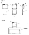
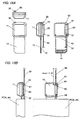
- FIG. 1 shows an antenna unit in accordance with a first embodiment of the present invention.
- the antenna unit is a GPS antenna unit, which is inserted into a SD card interface of an electronic device, such as a PDA, a notebook, etc., and receives a satellite signal from a GPS satellite, and sends data, such as an actual location, to the electronic device.
- a substrate 20 is housed in a section of the base 10 which is covered by the head cover 11.
- Signal processing modules constituted by many circuit elements are mounted on both surfaces of the substrate 20, and they are surrounded by an electromagnetic shields 21, 22 provided on the both surfaces of the substrate 20.
- An antenna 23 for receiving the satellite signal from the GPS satellite is fixed on the electromagnetic shield 21 on the upper surface side of the substrate 20, and the antenna 23 is electromagnetically isolated from the signal processing modules by the electromagnetic shields.
- the signal processing modules demodulate the satellite signal received by the antenna 23 into GPS signal and convert the GPS signal into signal data based on the protocol of the SD (Secure Digital) standard, and transmit the signal data to the electronic device through a terminal interface 40 which will be described later.
- a circuit ground 24, which forms a ground of the signal processing module, is formed across both of the surfaces of the substrate 20, and the electromagnetic shields 21, 22 are electrically connected to the circuit ground 24.
- a conductive stub piece 30 is connected to the electromagnetic shield 22 on the back side of the substrate 20.
- the stub piece 30 is made of a thin metal plate, and one end thereof is electrically connected to the electromagnetic shield and the other end thereof is a free end, that is, an electrical open end.
- the stub piece 30 is drawn from the base 10 to the outside through a hole 10A formed on the bottom of the base 10 (see FIG. 1 ), and then it is adhered to the base 10 and the head cover 11 along the outer surfaces thereof.
- the stub piece 30 will be described in more detail later.
- a terminal interface 40 is housed in a section of the base 10 which is covered by the interface cover 12.
- the terminal interface 40 comprises an lO substrate 40a, which is formed based on an interface standard for SD card, and flat cables 40b for connecting between the lO substrate 40a and the substrate 20.
- an array of terminals 41 which is adapted to be connected to an array of terminals provided in an interface of the electronic device when the antenna unit was inserted in the electronic device, is formed on the back side of the lO substrate 40a.
- the array of terminals 41 is exposed to the outside through a plurality of holes provided in the base 10.
- the array of terminals 41 includes a ground terminal which is adapted to be connected to a ground terminal of the electronic device.
- the flat cables 40b include a ground line 42 leading from the ground terminal to the circuit ground 24 of the substrate 20.
- the stub piece 30 constitutes a noise canceller for canceling noise generated in a CPU, etc. of the electronic device and transmitted to the circuit ground 24 through the ground terminal of the array of terminals 41 and the ground line 42.
- the length of the stub piece 30 is set to about 1/4 of a wavelength of the satellite signal.
- the length of the stub piece can be obtained by multiplying the wavelength ⁇ calculated by the above formula by 1/4. For example, when the frequency of the satellite signal received from the GPS satellite is about 1.6 GHz (about 1575.42 MHz), the length of the stub piece is in a range from 4.0 to 5.0 [cm], and preferably, the length is about 4.7 [cm].
- the length of the stub piece is in a range from 6.0 to 6.5 [cm], and preferably, the length is about 6.3 [cm].
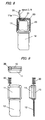
- the function of the stub piece will be described below with reference to FIG. 6 .
- the stub piece is described in a straight line shape, in FIG. 6 .
- the noise generated in the electronic device is transmitted to the electromagnetic shields 21, 22 and the antenna 23 through the ground terminal of the terminal interface 40, the ground line 42, and the circuit ground 24.
- the noise reached the electromagnetic shield 22 is branched to a branched noise (B) which runs through the stub piece 30 and a straight noise (A) which runs through the electromagnetic shield 22 without being branched.
- the branched noise (B) runs toward the free end of the stub piece 30, and is totally reflected at the free end, and returns to the electromagnetic shield 22. Since the length of the stub piece 30 is about 1/4 of the wavelength of the satellite signal, branched noise (B) having the same frequency as the satellite signal lags 180 degrees behind the straight noise (A) when the branched noise (B) goes to and from the stub piece 30 one time, namely, when the branched noise (B) travels a distance of one-half of the wavelength of the satellite signal. Therefore, the straight noise (A) and the branched noise (B) which has gone to and from the stub piece 30 cancel each other out, so the ground noise is reduced.
- the noise on the ground line exists over a wide range of frequencies
- the noise at about the same frequency as the satellite signal can be reduced by providing the stub piece 30 having the length of 1/4 of the wavelength of the satellite signal, and the ground level at the frequency of the satellite signal can be stabilized.
- the antenna unit having the stub piece 30 can receive the satellite signal with high sensitivity.
- the stub piece 30 can reduce noise generated in the antenna unit itself as well as the noise transmitted from the electronic device.
- the stub piece 30 is connected to the electromagnetic shield 22 on the back side of the substrate 20, the stub piece 30 may be connected to the electromagnetic shield 21 on the front side of the substrate 20 or to the circuit ground 24. That is, the stub piece 30 should just be electrically connected to a part where the noise on the ground is transmitted.
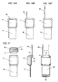
- the stub piece 30 of the present embodiment is made of a thin metal plate
- the stub piece 30 may be made of a wire, such as a lead wire, as shown in FIG. 7 .
- a wire such as a lead wire
- FIG. 8 one end of the wire is connected to the electromagnetic shield 21 by solder, etc., on the front side of the substrate 20, and the wire is extracted to the outside from a hole 11a provided in the head cover 11.
- the length of the wire from the one end thereof to the other end is about 1/4 of the wavelength of the satellite signal. In this case, because the wire is cheap, the increasing in cost necessary for the stub piece can be reduced.
- the stub piece does not project downward beyond the bottom of the case, therefore, the stub piece 30 will not receive an excessive pressure from a desk or a floor when the antenna unit is put on the desk or the floor, so, breakage of the stub piece 30 can be prevented.
- the front end of the stub piece 30 may be bent within a width of the case, as shown in FIG. 12 .
- the conductive surface 31 is engaged with the hardware 61, so that the stub piece 30 is electrically connected to the electromagnetic shield 22.
- the length of the stub piece 30 from the conductive surface 31, namely the lower end, to the tip thereof is about 1/4 of the wavelength of the satellite signal. In this case, while the stub piece 30 is housed in the receptacle 60, the stub piece 30 is not connected to the electromagnetic shield 22, so the stub piece 30 does not work as the noise canceller.
- the stub piece 30 is provided with a pushrod 32, which is made of a nonconductive material and extends from the bottom of the conductive surface 31 of the stub piece 30 and penetrates the bottom of the receptacle 60.
- a pushrod 32 which is made of a nonconductive material and extends from the bottom of the conductive surface 31 of the stub piece 30 and penetrates the bottom of the receptacle 60.
- the lower end of the pushrod 32 is pushed by a side surface of the electronic device, so that the stub piece 30 is automatically pulled up. Therefore, time and effort to pull up the stub piece 30 can be saved. Because the pushrod 32 is a nonconductor, it does not have an influence on the function of the noise canceller.
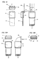
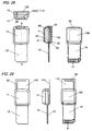
- the stub piece 30 may be the rod member and a receptacle 70 having an insertion hole 71 into which the lower end of the stub piece 30 can be inserted may be provided on the backside of the case.
- the inner surface of the insertion hole 71 is electrically connected to the electromagnetic shield 22.
- the conductive surface 31 is exposed to the outside at the lower end of the stub piece 30 and is electrically connected to the electromagnetic shield 22 through the inner surface of the insertion hole 71.
- the length of the stub piece 30 from the conductive surface 31 to the tip thereof is about 1/4 of the wavelength of the satellite signal.
- two or more receptacles 70 may be provided on the backside of the case, and the stub piece 30 may be inserted into the insertion hole 71 of any one of the receptacles 70.
- the inner surfaces of all insertion holes 71 are electrically connected to the electromagnetic shield 22.
- the conductive surface 31 is exposed to the outside at the lower end of the stub piece 30, and is electrically connected to the electromagnetic shield 22 through the inner surface of the insertion hole 71.
- the receiver sensitivity may be improved by shifting the insertion position of the stub piece 30 discontinuously.
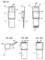
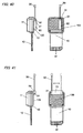
- the stub piece 30 may be a rod member whose one end is pivotally supported on the outer bottom of the case.
- the one end of the stub piece 30 is supported on the outer bottom of the case by a conductive screw 80.
- the tip of the screw 80 penetrates the base 10 and is electrically connected to the electromagnetic shield 22.
- the stub piece 30 is electrically connected to the electromagnetic shield 22 through the screw 80.
- the length of the stub piece 30 from the one end thereof to the tip is about 1/4 of the wavelength of the satellite signal.
- the screw 80 fixes the base 10 to the head cover 11 as well as supports the stub piece 30.
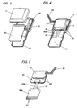
- the stub piece 30 can be hidden behind the case in a situation where the stub piece 30 gets in the way, for example, in a situation where the antenna unit is not used. Furthermore, it is easy to install the stub piece 30 because the stub piece 30 can be installed on the backside of the antenna unit after assembling the antenna unit. A stopper for restricting the rotation of the stub piece 30 may be provided on the case. If the stub piece can not be hidden behind the case, the stub piece 30 may be bent, as shown in FIG. 20 .
- the stub piece 30 is extended toward the interface cover 12 side, and is provided with a vertical plate 90 which electromagnetically insulates the antenna unit from the electronic device when the antenna unit is connected to the electronic device, namely when the antenna unit is inserted into the electronic device.
- a vertical plate 90 which electromagnetically insulates the antenna unit from the electronic device when the antenna unit is connected to the electronic device, namely when the antenna unit is inserted into the electronic device.
- the longitudinal length of a main body of the antenna unit is about 7cm
- the width thereof is about 3cm
- the height thereof is about 1.4 cm.
- the length and width of the stub piece 30 are about 7 cm, respectively, and the longitudinal length of the stub piece which projects from the head cover 11 in the plan view is about 4cm.
- the height of the vertical plate 90 is about 3 cm.
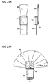
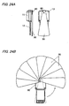
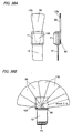
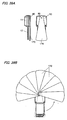
- the stub piece 30 is a fan-shaped plate, and the antenna unit is provided with two or more stub pieces as the noise canceller, and one end of each of the stub pieces 30 is pivotally supported on the outer bottom of the case by a screw 80.
- the tip of the screw 80 penetrates the base 10 and is electrically connected to the electromagnetic shield 22.
- the length of each of the stub pieces from the screw 80 to the front edge thereof is about 1/4 of the wavelength of the satellite signal.
- a user can spread those stub pieces 30 to one fan shape to give an uniform stub length over a predetermined direction around the antenna unit. Thus, the effect of reducing the noise can be enhanced.
- the stub pieces will not get in the way of the user by being grouped together while they are not used.
- FIG. 24A if the stub pieces 30 are fixed on the front edge side of the base 10, a user can hide the stub pieces 30 behind the case when the user does not use the stub pieces, so the stub pieces will not get in the way of the user more.
- the user wants to use the stub pieces 30, the user can rotate the stub pieces 180 degrees, and spread them to the fan shape, as shown in FIG. 24B .
- the antenna unit of the present invention is not limited to the GPS antenna unit.
- the antenna unit may be a LAN antenna unit which will be inserted into the electronic device such as a notebook and receive a wireless LAN signal and transmit the received signal to the electronic device.
- the antenna unit in this embodiment has an interface for a SD card, the unit may have an interface based on another standard, of course.
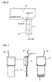
- FIG. 25 shows an antenna unit in accordance with a second embodiment of the present invention.
- the basic composition of this embodiment is identical to the first embodiment, so the similar part of these embodiments are identified by the same reference character and no duplicate explanation is made here.
- the noise generated in the electronic device is transmitted to the plate 100 capacitively coupled to the electromagnetic shield 22, through the ground terminal of the terminal interface 40, the ground line 42, and the circuit ground 24.
- a part of the noise transmitted to the plate 100 is branched to the stub piece 30 and is totally reflected at the free end of the stub piece 30.
- the noise branched to the stub piece 30 and the noise running through the plate 100 without being branched cancel each other out on the same principle as the first embodiment, so that the ground noise at about the same frequency as the satellite signal can be reduced.
- the antenna unit having the stub piece 30 can receive the satellite signal with high sensitivity.
- the noise canceller can be constructed by just bonding the plate 100 and the stub piece 30 to the case after assembling the antenna unit.
- the stub piece 30 may be formed from the same metal plate as the plate 100, as shown in FIG. 26 .
- the stub piece 30 may be formed from the plate 100 by cutting a part of the plate 100 and bending it. In this case, the material of the stub piece 30 can be reduced. If the stub piece 30 is too thin, the stub piece 30 is easily damaged. So, it is preferable that the stub piece 30 has a certain degree of thickness, if the stub piece 30 is used in a situation where it is exposed outwardly, not bonded to the outer surface of the head cover 11 as the stub piece of FIG. 25 . For information, even if the stub piece 30 is formed by cutting a part of the plate 100, it does not affect the capacity coupling between the plate 100 and the electromagnetic shield as long as the length of the stub piece is about 1/4 of the wavelength of the satellite signal.
- the stub piece 30 may be insert-molded into the case together with the plate 100.
- the plate 100 is insert-molded into the bottom of the base 10 so that it will make the capacity coupling with the electromagnetic shield 22.
- the stub piece 30 comprises two separate parts; a part which is extended from the plate 100 and insert-molded into the base 10, and a part insert-molded into the head cover 11. And, when the base 10 and the head cover 11 were assembled, these two parts are electrically connected to each other.
- the length from the connection between the plate 100 and the stub piece 30 to the tip of the stub piece 30 inside the head cover 11 is about 1/4 of the wavelength of the satellite signal. In this case, the number of parts can be reduced, thus it becomes easy to assemble the antenna unit.
- the antenna unit may further include a thin and nonconductive sheet 110.
- the sheet 110 is attached to the outer bottom of the case, and the plate 100 and the stub piece 30 are formed in the sheet 110.
- the plate 100 is capacitively coupled to the electromagnetic shield 22 through the bottom of the base 10 when the sheet 110 is attached to the outer bottom of the case.
- the noise canceller can be constructed by just attaching the sheet 110 to the case after assembling the antenna unit.
- the shape of the stub piece 30 in the sheet 110 may be a meander shape as shown in FIG. 30 , or may be a convoluted shape as shown in FIG. 31 . In each case, the overhang of the sheet 110 can be shortened.
- one or more perforations 120 along which the end of the stub piece 30 can be torn are made on the sheet 110.
- the length of the stub piece 30 can be adjusted by tearing the end of the stub piece 30 from the sheet, so that a user can select a proper length of the stub piece with respect to the satellite signals of different frequencies (for example, about 1.6 GHz or 1.2 GHz).
- the shape of the sheet 110 is not limited to a rectangle, but it may be a shape which was cut out along the shape of the plate 100 and the stub piece 30, as shown in FIG. 33A .
- the sheet 110 can be pasted on the outer surface of the case, so that the overhang of the sheet 110 can be eliminated.
- one or more perforations 120 along which the end of the stub piece 30 can be torn may be made on the sheet 110, as shown in FIG. 33A , so as to adjust the length of the stub piece, as shown in FIG. 33C .
- the stub piece 30 may be divided into two or more in the sheet 110, and as shown in FIG. 34B , the divided stub pieces 30 may be connected to each other by a conductive jumper 130, if needed.
- a user can select a proper length of the stub piece according to the wavelength of the satellite signal by attaching the jumper 130 or removing it.
- the antenna unit may be provided with a plastic case cover 140, which can be attached to the outer bottom of the case as well as the side faces of the head cover 11, and the plate 100 and the stub piece 30 may be insert-molded into the case cover 140.
- the plate 100 is disposed on the bottom of the case cover 140, and, as shown in FIG. 35B , when the case cover 140 was attached to the outer bottom of the case, the plate 100 will be capacitively coupled to the electromagnetic shield 22 through the base 10.
- the noise canceller can be constructed by just attaching the case cover 140 to the antenna unit, the noise cancellation function can be easily added to the conventional antenna unit.
- the stub piece may be in a form of a flat plate extending from the plate 100 attached to the outer bottom of the case. That is, the plate 100 and the stub piece 30 may be a single conductive flat plate 150 attached to the outer bottom of the case.
- the length of the section of the flat plate 150 projecting from the base 10 is about 1/4 of the wavelength of the satellite signal.
- the shape of the stub piece 30 is not limited to the line shape (the straight line shape or the curved line shape), but it may be in the form of the flat plate.
- the plate 100 is provided with a vertical plate 160 on the other side of the stub piece 30, which electromagnetically insulates the antenna unit from the electronic device when the antenna unit is connected to the electronic device, namely when the antenna unit is inserted into the electronic device. In this case, it becomes easy to block the noise propagated to the antenna unit from the electronic device through midair by the vertical plate 160, so the unit can enhance the effect of reducing the noise.
- the length of the section of the plate 170 projecting from the base 10, that is, the section which acts as the stub piece, is about 1/4 of the wavelength of the satellite signal.
- FIG. 39A when the plate 170 are fixed on the front edge side of the base 10, a user can hide the plate 170 behind the case while they are not used, so the plate 170 will not get in the way of the user more.
- FIG. 39B when a user wants to use the stub pieces 30, the user can rotate the plate 180 degrees and spread them to the fan shape.
- FIG. 40 shows a modified form based on FIG. 14B of the first embodiment.
- the hardware 61 is electrically connected to the plate 100, not to the electromagnetic shield 22, and the stub piece 30 is electrically connected to the electromagnetic shield 22 through the hardware 61 and the plate 100.
- FIG. 41 shows a modified form based on FIG. 17 of the first embodiment. In FIG.
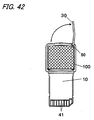
- FIG. 42 shows a modified form of FIG. 19A in the first embodiment.
- the screw 80 is electrically connected to the plate 100
- the stub piece 30 is electrically connected to the electromagnetic shield 22 through the screw 80 and the plate 100.
Landscapes
- Engineering & Computer Science (AREA)
- Computer Networks & Wireless Communication (AREA)
- Computer Hardware Design (AREA)
- General Engineering & Computer Science (AREA)
- Physics & Mathematics (AREA)
- Electromagnetism (AREA)
- Signal Processing (AREA)
- Support Of Aerials (AREA)
- Details Of Aerials (AREA)
- Shielding Devices Or Components To Electric Or Magnetic Fields (AREA)
Claims (17)
- Mit einer elektronischen Einrichtung verbindbare Anntenneneinheit zum Senden eines empfangenen Funksignals zur elektronischen Einrichtung, mit:- einer zum Empfang eines Funksignals ausgebildeten Antenne (23);- einem zum Umwandeln des durch die Antenne (23) empfangenen Funksignals in zur elektronischen Einrichtung zu sendende Signaldaten ausgebildeten Signalverarbeitungsmodul;- einem zum Tragen der Antenne (23) und des Signalverarbeitungsmoduls ausgebildeten Substrat (20), wobei das Substrat (20) eine Schaltungsmasse (24) aufweist, die eine Masse des Signalverarbeitungsmoduls bildet;- einer zum Besitzen eines Felds von Anschlüssen (41) für eine elektrische Verbindung mit der elektronischen Einrichtung ausgebildeten Anschlussschnittstelle (40),wobei die Anschlussschnittstelle (40) eine Masseleitung (42) enthält, die von einem in dem Feld von Anschlüssen (41) ausgebildeten Masseanschluss zu der Schaltungsmasse (24) führt;- einer zum Umgeben des Signalverarbeitungsmoduls ausgebildeten elektromagnetischen Abschirmung (21, 22), um das Signalverarbeitungsmodul elektromagnetisch von der Antenne (23) zu isolieren, wobei die elektromagnetische Abschirmung (21, 22) elektrisch mit der Schaltungsmasse (24) verbunden ist;einem Gehäuse, hergestellt aus isolierendem Harz, wobei das Gehäuse ausgebildet ist, die Antenne, das Substrat (20), das Signalverarbeitungsmodul, die Anschlussschnittstelle (40) und die elektromagnetische Abschirmung (21, 22) aufzunehmen, während das Feld von Anschlüssen (41) freigelegt ist;
dadurch gekennzeichnet, dass
die Antenneneinheit einen Rauschbeseitiger zur Beseitigung von in der elektronischen Einrichtung erzeugtem und über die Masseleitung (42) zur Schaltungsmasse (24) übertragenem Rauschen enthält;
wobei der Rauschbeseitiger ein leitfähiges Stichleitungsstück (30) aufweist, dessen eines Ende elektrisch mit der elektromagnetischen Abschirmung (21, 22) verbunden ist, und dessen anderes Ende ein freies Ende ist, wobei das Stichleitungsstück (30) eine Länge von ungefähr ¼ einer Wellenlänge des Funksignals besitzt. - Antenneneinheit nach Anspruch 1, wobei
das Stichleitungsstück (30) aus einem Draht hergestellt ist. - Antenneneinheit nach Anspruch 1, wobei
das Stichleitungsstück (30) durch Schneiden eines Teils der elektromagnetischen Abschirmung (21) und Biegen davon formbar ist. - Antenneneinheit nach Anspruch 1, wobei
das Stichleitungsstück (30) ein Stabelement ist, das relativ zum Gehäuse ausdehnbar ist. - Antenneneinheit nach Anspruch 1, wobei
das Stichleitungsstück (30) ein Stabelement ist;
das Gehäuse eine Aufnahme (60) an einem äußeren Boden davon besitzt, deren innere Oberfläche elektrisch mit der elektromagnetischen Abschirmung verbunden ist;
ein Ende des Stichleitungsstücks (30) in die Aufnahme (60) eingefügt und durch die innere Oberfläche der Aufnahme (60) elektrisch mit der elektromagnetischen Abschirmung (22) verbunden ist. - Antenneneinheit nach Anspruch 1, wobei
das Stichleitungsstück (30) ein Stabelement ist, dessen eines Ende drehbar auf dem äußeren Boden des Gehäuses gelagert ist. - Antenneneinheit nach Anspruch 1, wobei
das Stichleitungsstück (30) in der Form einer flachen Platte ist. - Antenneneinheit nach Anspruch 7, wobei
das Stichleitungsstück (30) an einem äußeren Boden des Gehäuses angeordnet und mit einer vertikalen Platte versehen ist, die die Antenneneinheit elektromagnetisch von der elektronischen Einrichtung isoliert, wenn die Antenneneinheit mit der elektronischen Einrichtung verbunden ist. - Antenneneinheit nach Anspruch 7, wobei
das Stichleitungsstück (30) in Form eines Fächers ist;
der Rauschbeseitiger eines oder mehrere Stichleitungsstücke (30) aufweist;
ein Ende jedes Stichleitungsstücks drehbar auf einem äußeren Boden des Gehäuses gelagert ist. - Antenneneinheit nach Anspruch 1, wobei
die elektromagnetische Abschirmung (21, 22) auf einem inneren Boden des Gehäuses angeordnet ist;
die Antenneneinheit weiterhin eine Platte aufweist, die kapazitiv durch einen Boden des Gehäuses mit der elektromagnetischen Abschirmung verbunden ist;
ein Ende des Stichleitungsstücks mit der Platte verbunden ist und das Stichleitungsstück durch die Platte elektrisch mit der elektromagnetischen Abschirmung verbunden ist. - Antenneneinheit nach Anspruch 10, wobei
die Platte an einem äußeren Boden des Gehäuses befestigt ist;
das Stichleitungsstück (30) durch Schneiden eines Teils der Platte und Biegen davon gebildet ist. - Antenneneinheit nach Anspruch 10, wobei
das Stichleitungsstück (30) zusammen mit der Platte in das Gehäuse einfügeschmelzbar ist. - Antenneneinheit nach Anspruch 10, weiterhin mit
einem an einem äußeren Boden des Gehäuses befestigtem Blattelement;
wobei die Platte und das Stichleitungsstück (30) in dem Blatt gebildet sind. - Antenneneinheit nach Anspruch 10, weiterhin mit
einer an dem äußeren Boden des Gehäuses befestigten Gehäuseabdeckung;
wobei die Platte und das Stichleitungsstück (30) in die Gehäuseabdeckung einfügegeschmolzen sind. - Antenneneinheit nach Anspruch 10, wobei
die Platte an einem äußeren Boden des Gehäuses befestigt ist;
das Stichleitungsstück (30) in einer Form einer flachen Platte ist, die sich von der Platte erstreckt. - Antenneneinheit nach Anspruch 15, wobei
die Platte mit einer vertikalen Platte versehen ist, die die Antenneneinheit elektromagnetisch von der elektronischen Einrichtung isoliert, wenn die Antenneneinheit mit der elektronischen Einrichtung verbunden ist. - Antenneneinheit nach Anspruch 15, wobei
die Platte und das Stichleitungsstück (30) eine fächerförmige Platte sind;
wobei der Rauschbeseitiger zwei oder mehr fächerförmige Platten aufweist, wobei ein Ende jeder der der fächerförmigen Platten drehbar auf dem äußeren Boden des Gehäuses gelagert ist.
Applications Claiming Priority (3)
| Application Number | Priority Date | Filing Date | Title |
|---|---|---|---|
| JP2004040308 | 2004-02-17 | ||
| JP2004040308 | 2004-02-17 | ||
| PCT/JP2004/015782 WO2005078971A1 (ja) | 2004-02-17 | 2004-10-25 | アンテナユニット |
Publications (3)
| Publication Number | Publication Date |
|---|---|
| EP1589680A1 EP1589680A1 (de) | 2005-10-26 |
| EP1589680A4 EP1589680A4 (de) | 2006-09-13 |
| EP1589680B1 true EP1589680B1 (de) | 2008-02-27 |
Family
ID=34857877
Family Applications (1)
| Application Number | Title | Priority Date | Filing Date |
|---|---|---|---|
| EP04792919A Expired - Lifetime EP1589680B1 (de) | 2004-02-17 | 2004-10-25 | Antenneneinheit |
Country Status (5)
| Country | Link |
|---|---|
| US (1) | US7176839B2 (de) |
| EP (1) | EP1589680B1 (de) |
| DE (1) | DE602004012067T2 (de) |
| TW (1) | TWI249910B (de) |
| WO (1) | WO2005078971A1 (de) |
Families Citing this family (11)
| Publication number | Priority date | Publication date | Assignee | Title |
|---|---|---|---|---|
| DE602005002697T2 (de) | 2004-08-21 | 2008-01-24 | Samsung Electronics Co., Ltd., Suwon | Kleine Planarantenne mit erhöhter Bandbreite und kleine Streifenantenne |
| JP2008160784A (ja) * | 2006-11-29 | 2008-07-10 | Kyocera Corp | 無線通信機器 |
| JP5239556B2 (ja) * | 2008-07-01 | 2013-07-17 | 富士通株式会社 | 成型品 |
| EP2249432A1 (de) * | 2009-05-07 | 2010-11-10 | Gemalto SA | Vorrichtung zur Ausstattung eines Endgeräts mit allen oder einem Teil der Funkfunktionen |
| JP2011119949A (ja) * | 2009-12-02 | 2011-06-16 | Mitsumi Electric Co Ltd | カードデバイス |
| US8299372B2 (en) | 2010-06-11 | 2012-10-30 | Laird Technologies, Inc. | Antenna universal mount joint connectors |
| JP5862163B2 (ja) * | 2011-09-28 | 2016-02-16 | 日産自動車株式会社 | 電力変換装置 |
| TWI538300B (zh) * | 2014-01-27 | 2016-06-11 | A resonant circuit capable of suppressing the interference between the high-frequency connector and the antenna | |
| US20170063011A1 (en) * | 2015-08-24 | 2017-03-02 | Electronic Product Solutions LLC | CFast Card Slot Breakout Cable |
| FR3042916B1 (fr) * | 2015-10-22 | 2017-12-01 | Peugeot Citroen Automobiles Sa | Dispositif d’affichage a ecran tactile a emission electromagnetique interferante reduite |
| CN105356058B (zh) * | 2015-11-26 | 2019-03-29 | 联想(北京)有限公司 | 一种电子设备及天线装置 |
Family Cites Families (8)
| Publication number | Priority date | Publication date | Assignee | Title |
|---|---|---|---|---|
| GB2101412B (en) * | 1981-06-30 | 1985-04-11 | Rca Corp | Rf shielding apparatus |
| US5606732A (en) * | 1994-04-26 | 1997-02-25 | Rockwell International Corporation | Direct connect radio and antenna assembly |
| JPH11298202A (ja) | 1998-04-09 | 1999-10-29 | Murata Mfg Co Ltd | バンドパスフィルタ及び2逓倍回路 |
| JP2000292522A (ja) * | 1999-04-12 | 2000-10-20 | Japan Radio Co Ltd | 測位カード |
| US6539207B1 (en) * | 2000-06-27 | 2003-03-25 | Symbol Technologies, Inc. | Component for a wireless communications equipment card |
| JP2003180431A (ja) | 2001-12-17 | 2003-07-02 | Eisuke Fujimoto | Pda用書類鞄 |
| JP2004363392A (ja) * | 2003-06-05 | 2004-12-24 | Hitachi Ltd | プリント配線基板および無線通信装置 |
| TW572378U (en) * | 2003-06-25 | 2004-01-11 | Quanta Comp Inc | Electronic device and its three-dimensional antenna structure |
-
2004
- 2004-10-25 DE DE602004012067T patent/DE602004012067T2/de not_active Expired - Fee Related
- 2004-10-25 US US10/536,981 patent/US7176839B2/en not_active Expired - Fee Related
- 2004-10-25 WO PCT/JP2004/015782 patent/WO2005078971A1/ja not_active Ceased
- 2004-10-25 EP EP04792919A patent/EP1589680B1/de not_active Expired - Lifetime
- 2004-10-29 TW TW093133133A patent/TWI249910B/zh not_active IP Right Cessation
Also Published As
| Publication number | Publication date |
|---|---|
| TW200529579A (en) | 2005-09-01 |
| EP1589680A4 (de) | 2006-09-13 |
| DE602004012067T2 (de) | 2009-03-05 |
| WO2005078971A1 (ja) | 2005-08-25 |
| DE602004012067D1 (de) | 2008-04-10 |
| US7176839B2 (en) | 2007-02-13 |
| TWI249910B (en) | 2006-02-21 |
| EP1589680A1 (de) | 2005-10-26 |
| US20060007046A1 (en) | 2006-01-12 |
Similar Documents
| Publication | Publication Date | Title |
|---|---|---|
| US5677698A (en) | Slot antenna arrangement for portable personal computers | |
| US5699319A (en) | Horlogical piece comprising an antenna | |
| US6285327B1 (en) | Parasitic element for a substrate antenna | |
| EP1589680B1 (de) | Antenneneinheit | |
| EP1102347B1 (de) | Integrierte Antennenerdungsplatte und EMV- Abschirmstruktur | |
| US6218991B1 (en) | Compact planar inverted F antenna | |
| EP2546922B1 (de) | Mobiles Kommunikationsgerät und Antennenvorrichtung | |
| US20100149751A1 (en) | Electronic device antenna | |
| EP1093675B1 (de) | Substratantenne mit einem element zur verhinderung von energiekopplung zwischen antenne und leitern | |
| EP1247311A1 (de) | Antennenanordnungund verffahrenzur befestigung einer derartigen antennenanordnung | |
| MX2008004942A (es) | Terminal movil que tiene una antena interna mejorada. | |
| EP2270921A1 (de) | Verbundantennenvorrichtung | |
| US6362786B1 (en) | Patch antenna utilized in conjunction with an electronic apparatus | |
| CN112787077A (zh) | 天线辐射体及电子设备 | |
| US20120146876A1 (en) | Surface mount device antenna module | |
| EP1181742B1 (de) | Antennenanrodnung, funkkommunikationssystem und verfahren zur herstellung einer strahlenstruktur | |
| CN114982061B (zh) | 背腔式边框天线 | |
| EP4386980A1 (de) | Antennenanordnung für einen drahtlosen ohrcomputer | |
| EP1732161B1 (de) | Interne Antenne und mobiles Kommunikationsgerät mit solch einer Antenne | |
| CN112886211B (zh) | 穿戴式电子设备 | |
| JP4710327B2 (ja) | アンテナユニット | |
| EP1863120B1 (de) | Fahrzeugantennenvorrichtung | |
| WO2002037603A1 (en) | Antenna arrangement | |
| JP2002353733A (ja) | 無線端末装置 | |
| JP2743840B2 (ja) | パーソナルコンピュータのための無線データ通信装置 |
Legal Events
| Date | Code | Title | Description |
|---|---|---|---|
| PUAI | Public reference made under article 153(3) epc to a published international application that has entered the european phase |
Free format text: ORIGINAL CODE: 0009012 |
|
| 17P | Request for examination filed |
Effective date: 20050527 |
|
| AK | Designated contracting states |
Kind code of ref document: A1 Designated state(s): AT BE BG CH CY CZ DE DK EE ES FI FR GB GR HU IE IT LI LU MC NL PL PT RO SE SI SK TR |
|
| AX | Request for extension of the european patent |
Extension state: AL HR LT LV MK |
|
| A4 | Supplementary search report drawn up and despatched |
Effective date: 20060816 |
|
| 17Q | First examination report despatched |
Effective date: 20061108 |
|
| DAX | Request for extension of the european patent (deleted) | ||
| RBV | Designated contracting states (corrected) |
Designated state(s): DE GB |
|
| GRAP | Despatch of communication of intention to grant a patent |
Free format text: ORIGINAL CODE: EPIDOSNIGR1 |
|
| GRAS | Grant fee paid |
Free format text: ORIGINAL CODE: EPIDOSNIGR3 |
|
| GRAA | (expected) grant |
Free format text: ORIGINAL CODE: 0009210 |
|
| AK | Designated contracting states |
Kind code of ref document: B1 Designated state(s): DE GB |
|
| REG | Reference to a national code |
Ref country code: GB Ref legal event code: FG4D |
|
| REF | Corresponds to: |
Ref document number: 602004012067 Country of ref document: DE Date of ref document: 20080410 Kind code of ref document: P |
|
| PLBE | No opposition filed within time limit |
Free format text: ORIGINAL CODE: 0009261 |
|
| STAA | Information on the status of an ep patent application or granted ep patent |
Free format text: STATUS: NO OPPOSITION FILED WITHIN TIME LIMIT |
|
| PGFP | Annual fee paid to national office [announced via postgrant information from national office to epo] |
Ref country code: DE Payment date: 20081027 Year of fee payment: 5 |
|
| 26N | No opposition filed |
Effective date: 20081128 |
|
| PGFP | Annual fee paid to national office [announced via postgrant information from national office to epo] |
Ref country code: GB Payment date: 20081022 Year of fee payment: 5 |
|
| PG25 | Lapsed in a contracting state [announced via postgrant information from national office to epo] |
Ref country code: DE Free format text: LAPSE BECAUSE OF NON-PAYMENT OF DUE FEES Effective date: 20100501 |
|
| PG25 | Lapsed in a contracting state [announced via postgrant information from national office to epo] |
Ref country code: GB Free format text: LAPSE BECAUSE OF NON-PAYMENT OF DUE FEES Effective date: 20091025 |