EP1589618A1 - Appareil électrique avec borne de contact et méthode de production - Google Patents
Appareil électrique avec borne de contact et méthode de production Download PDFInfo
- Publication number
- EP1589618A1 EP1589618A1 EP05103244A EP05103244A EP1589618A1 EP 1589618 A1 EP1589618 A1 EP 1589618A1 EP 05103244 A EP05103244 A EP 05103244A EP 05103244 A EP05103244 A EP 05103244A EP 1589618 A1 EP1589618 A1 EP 1589618A1
- Authority
- EP
- European Patent Office
- Prior art keywords
- contact pin
- hole
- board
- pad
- electronic device
- Prior art date
- Legal status (The legal status is an assumption and is not a legal conclusion. Google has not performed a legal analysis and makes no representation as to the accuracy of the status listed.)
- Withdrawn
Links
Images

Classifications
-
- H—ELECTRICITY
- H05—ELECTRIC TECHNIQUES NOT OTHERWISE PROVIDED FOR
- H05K—PRINTED CIRCUITS; CASINGS OR CONSTRUCTIONAL DETAILS OF ELECTRIC APPARATUS; MANUFACTURE OF ASSEMBLAGES OF ELECTRICAL COMPONENTS
- H05K1/00—Printed circuits
- H05K1/02—Details
- H05K1/11—Printed elements for providing electric connections to or between printed circuits
- H05K1/115—Via connections; Lands around holes or via connections
- H05K1/116—Lands, clearance holes or other lay-out details concerning the surrounding of a via
-
- H—ELECTRICITY
- H01—ELECTRIC ELEMENTS
- H01R—ELECTRICALLY-CONDUCTIVE CONNECTIONS; STRUCTURAL ASSOCIATIONS OF A PLURALITY OF MUTUALLY-INSULATED ELECTRICAL CONNECTING ELEMENTS; COUPLING DEVICES; CURRENT COLLECTORS
- H01R12/00—Structural associations of a plurality of mutually-insulated electrical connecting elements, specially adapted for printed circuits, e.g. printed circuit boards [PCB], flat or ribbon cables, or like generally planar structures, e.g. terminal strips, terminal blocks; Coupling devices specially adapted for printed circuits, flat or ribbon cables, or like generally planar structures; Terminals specially adapted for contact with, or insertion into, printed circuits, flat or ribbon cables, or like generally planar structures
- H01R12/50—Fixed connections
- H01R12/51—Fixed connections for rigid printed circuits or like structures
- H01R12/55—Fixed connections for rigid printed circuits or like structures characterised by the terminals
- H01R12/58—Fixed connections for rigid printed circuits or like structures characterised by the terminals terminals for insertion into holes
-
- H—ELECTRICITY
- H01—ELECTRIC ELEMENTS
- H01R—ELECTRICALLY-CONDUCTIVE CONNECTIONS; STRUCTURAL ASSOCIATIONS OF A PLURALITY OF MUTUALLY-INSULATED ELECTRICAL CONNECTING ELEMENTS; COUPLING DEVICES; CURRENT COLLECTORS
- H01R43/00—Apparatus or processes specially adapted for manufacturing, assembling, maintaining, or repairing of line connectors or current collectors or for joining electric conductors
- H01R43/02—Apparatus or processes specially adapted for manufacturing, assembling, maintaining, or repairing of line connectors or current collectors or for joining electric conductors for soldered or welded connections
- H01R43/0256—Apparatus or processes specially adapted for manufacturing, assembling, maintaining, or repairing of line connectors or current collectors or for joining electric conductors for soldered or welded connections for soldering or welding connectors to a printed circuit board
-
- H—ELECTRICITY
- H05—ELECTRIC TECHNIQUES NOT OTHERWISE PROVIDED FOR
- H05K—PRINTED CIRCUITS; CASINGS OR CONSTRUCTIONAL DETAILS OF ELECTRIC APPARATUS; MANUFACTURE OF ASSEMBLAGES OF ELECTRICAL COMPONENTS
- H05K2201/00—Indexing scheme relating to printed circuits covered by H05K1/00
- H05K2201/09—Shape and layout
- H05K2201/09209—Shape and layout details of conductors
- H05K2201/09372—Pads and lands
- H05K2201/0949—Pad close to a hole, not surrounding the hole
-
- H—ELECTRICITY
- H05—ELECTRIC TECHNIQUES NOT OTHERWISE PROVIDED FOR
- H05K—PRINTED CIRCUITS; CASINGS OR CONSTRUCTIONAL DETAILS OF ELECTRIC APPARATUS; MANUFACTURE OF ASSEMBLAGES OF ELECTRICAL COMPONENTS
- H05K2201/00—Indexing scheme relating to printed circuits covered by H05K1/00
- H05K2201/10—Details of components or other objects attached to or integrated in a printed circuit board
- H05K2201/10227—Other objects, e.g. metallic pieces
- H05K2201/10295—Metallic connector elements partly mounted in a hole of the PCB
- H05K2201/10303—Pin-in-hole mounted pins
-
- H—ELECTRICITY
- H05—ELECTRIC TECHNIQUES NOT OTHERWISE PROVIDED FOR
- H05K—PRINTED CIRCUITS; CASINGS OR CONSTRUCTIONAL DETAILS OF ELECTRIC APPARATUS; MANUFACTURE OF ASSEMBLAGES OF ELECTRICAL COMPONENTS
- H05K2201/00—Indexing scheme relating to printed circuits covered by H05K1/00
- H05K2201/10—Details of components or other objects attached to or integrated in a printed circuit board
- H05K2201/10431—Details of mounted components
- H05K2201/1059—Connections made by press-fit insertion
-
- H—ELECTRICITY
- H05—ELECTRIC TECHNIQUES NOT OTHERWISE PROVIDED FOR
- H05K—PRINTED CIRCUITS; CASINGS OR CONSTRUCTIONAL DETAILS OF ELECTRIC APPARATUS; MANUFACTURE OF ASSEMBLAGES OF ELECTRICAL COMPONENTS
- H05K2201/00—Indexing scheme relating to printed circuits covered by H05K1/00
- H05K2201/10—Details of components or other objects attached to or integrated in a printed circuit board
- H05K2201/10613—Details of electrical connections of non-printed components, e.g. special leads
- H05K2201/10742—Details of leads
- H05K2201/1075—Shape details
- H05K2201/10871—Leads having an integral insert stop
-
- H—ELECTRICITY
- H05—ELECTRIC TECHNIQUES NOT OTHERWISE PROVIDED FOR
- H05K—PRINTED CIRCUITS; CASINGS OR CONSTRUCTIONAL DETAILS OF ELECTRIC APPARATUS; MANUFACTURE OF ASSEMBLAGES OF ELECTRICAL COMPONENTS
- H05K3/00—Apparatus or processes for manufacturing printed circuits
- H05K3/30—Assembling printed circuits with electric components, e.g. with resistors
- H05K3/306—Assembling printed circuits with electric components, e.g. with resistors with lead-in-hole components
- H05K3/308—Adaptations of leads
-
- H—ELECTRICITY
- H05—ELECTRIC TECHNIQUES NOT OTHERWISE PROVIDED FOR
- H05K—PRINTED CIRCUITS; CASINGS OR CONSTRUCTIONAL DETAILS OF ELECTRIC APPARATUS; MANUFACTURE OF ASSEMBLAGES OF ELECTRICAL COMPONENTS
- H05K3/00—Apparatus or processes for manufacturing printed circuits
- H05K3/30—Assembling printed circuits with electric components, e.g. with resistors
- H05K3/32—Assembling printed circuits with electric components, e.g. with resistors electrically connecting electric components or wires to printed circuits
- H05K3/34—Assembling printed circuits with electric components, e.g. with resistors electrically connecting electric components or wires to printed circuits by soldering
- H05K3/3447—Lead-in-hole components
Definitions
- the present invention relates to an electronic device with a contact pin.
- the present invention relates to an electronic device of the type comprising a printed circuit board (PCB) fitted with contact pins.
- PCB printed circuit board
- Electronic devices of this sort are used as straightforward connectors or as actual processing boards when fitted with circuit components such as capacitors, resistors, diodes, etc..
- Printed circuits are normally formed on a board made of FR-4, i.e. a material comprising glass fibre and epoxy resin with a glass transition temperature of 135°C.
- the board is punched to form through holes, and has a first and second side, which are plated with respective copper plates on which the circuits are formed by etching conducting tracks and pads.
- the inner faces of the through holes are then plated by electrodeposition to form an electrical contact between the circuits on the first and second sides and to make the inner faces of the holes conductive (PTH : plated through holes).
- PTH plated through holes
- the elongated portion In use, the elongated portion must be maintained perpendicular to the board, while the arms define the position in which the pin rests on the board.
- Part of the elongated portion is located inside the plated through hole, and has a central through slit forming two rods, which are outwardly convex to exert elastic force on the wall of the through hole when inserted inside the through hole. Between the two rods, some contact pins have resilient mechanisms for pushing the rods outwards. The elasticity of the rods provides for forming a mechanical fit and electrical contact between the contact pin and the plated face of the through hole.
- the present invention also relates to a method of producing an electronic device.
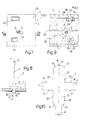
- Number 1 in Figure 1 indicates as a whole an electronic device having a printed circuit board PCB1 comprising a board 2.
- board 2 comprises a side 3, and a side 4 parallel to side 3 so as to define a substantially constant thickness L; and a through hole 5 bounded by a face 6 (Figure 3).
- side 3 is copper plated, and tracks 7 and two pads 8 are etched on diametrically opposite sides of hole 5.
- printed circuit board PCB1 comprises a number of holes 5 and pads 8.
- Each pad 8 is substantially oval and located a distance from the edge of hole 5.
- the device also comprises an elongated contact pin 9 extending along an axis 10 perpendicular, in use, to sides 3 and 4 of board 2.
- Pin 9 is blanked from sheet metal and is normally rectangular in cross section.
- contact pin 9 is substantially cross-shaped, and comprises two arms 11 perpendicular to axis 10; two fastening portions 12 and 13; and a connecting portion 14.
- Portions 12, 13, 14 are arranged successively along axis 10. More specifically, fastening portions 12 and 13 are located on opposite sides of arms 11, while portion 14, which is smaller in cross section than portion 13, is connected to portion 13 by two faces 15 sloping with respect to axis 10. Each arm 11 has a face 16 and a face 17, which are perpendicular to axis 10 and are positioned contacting a respective pad 8.
- portion 12 is defined by a face 18 perpendicular to axis 10, and by two inclined lateral faces 19; portions 12 and 13 have edges 20 which cooperate with inner face 6 of hole 5; and portion 14 has a tapered outer end 21 for easy insertion of portion 14.
- Figure 3 shows the cross section of portion 13 contacting inner face 6 of hole 5 along edges 20; and Figure 4 shows the cross section of portion 14 smaller than the cross section of portion 13.
- Number 22 in Figure 1 indicates electronic components, such as diodes, capacitors, resistors, etc., fitted to side 3 of board 2.
- the method of producing device 1 comprises plating board 2 along side 3 only, and forming tracks 7 and pads 8; contact pins 9 and electronic components 22 are then inserted on the same side, i.e. side 3; and contact pins 9 are then SMT (surface mounting technology) soldered.
- SMT comprises applying small amounts of soldering paste to the areas to be joined, such as arms 11 and pads 8; after which, board 2 is placed inside an oven where the soldering paste adheres to pads 8 and arms 11 to form the electrical contact between contact pin 9 and pad 8, i.e. the printed circuit.
- board 2 is only plated along side 3, so that holes 5 cannot be plated, and components 22 are inserted and soldered on side 3 only, so that, throughout the production process, board 2 is never turned over, thus saving considerable time.
- contact between contact pin 9 and face 6 of the hole serves solely to keep contact pin 9 perpendicular to board 2, and the insertion forces are reduced, so that board 2 may be made of CEM 1 or CEM 3, which have a lower mechanical resistance than FR-4 and are decidedly cheaper.
- contact pin 9 is blanked from a sheet metal strip and is therefore much cheaper than round-section contacts.
- the two pads 8 have the advantage of limiting flow of the soldering paste along the relatively small pad 8, and of preventing the soldering paste from flowing into hole 5.
- the soldering paste in fact, flows along the metal pad, but is halted by the rougher surface of board 2.
- number 23 indicates an electronic device, which differs from device 1 by board PCB1 being replaced by a board PCB2, and by contact pin 9 being inserted by portion 12.
- Board PCB2 in turn differs from board PCB1 by pads 8 being replaced by a single pad 24, which extends about hole 5 and is substantially rectangular with two curved areas 25 located along the long sides with their convexities facing away from hole 5.
- Portion 12 is inserted inside hole 5 with relative edges 20 contacting inner face 6 of the hole to form the mechanical fit. Faces 16 of the arms contact pad 24, and arms 11 are SMT soldered to pad 24.
- Electronic device 23 is produced using substantially the same method as described for electronic device 1, except that fastening portion 12 is inserted inside hole 5 instead of fastening portion 13.
- number 26 indicates an electronic device comprising a printed circuit board PCB3, which has numerous elements in common with printed circuit board PCB1 as described above, and which are indicated using the same reference numbers as for the corresponding elements of board PCB1.
- board PCB3 also comprises an annular pad 27 surrounding hole 5 on side 4 of board 2 ( Figure 9).
- Electronic device 26 also differs from devices 1 and 23 by components 22 comprising fastening pins 28 engaging respective through holes in board 2.
- a pad 29 surrounds each hole on side 4 to fasten pins 28 of components 22.
- Conducting tracks 7 are also formed on side 4, which is covered with a transparent protective layer 30 except for pads 27 and 29.
- the method of producing electronic device 26 comprises plating board 2 on side 4, and forming tracks 7 and pads 27 and 29 on side 4.
- Contact pin 9 is inserted inside hole 5 and pins 28 of electronic components 22 are inserted inside respective holes on the same side, i.e. side 3, and are then flow soldered on side 4.
- flow soldering comprises sweeping side 4 with a wave formed in a bath of molten metal, which adheres to the metal parts : pads 27 and 29, faces 18 and 19 of contact pin 9, and the projecting parts of the pins of components 22, to form the respective joints.
- portion 12 inserted forcefully inside hole 5 provides for mechanical fit, while soldering contact pin 9, which in this case is soldered between faces 18, 19 and pad 27, provides for electrical contact.
Landscapes
- Engineering & Computer Science (AREA)
- Manufacturing & Machinery (AREA)
- Microelectronics & Electronic Packaging (AREA)
- Coupling Device And Connection With Printed Circuit (AREA)
Applications Claiming Priority (2)
| Application Number | Priority Date | Filing Date | Title |
|---|---|---|---|
| ITMI20040805 | 2004-04-23 | ||
| IT000805A ITMI20040805A1 (it) | 2004-04-23 | 2004-04-23 | Dispositivo elettronico provvisto di un piedino di contatto e metodo di realizzazione di tale dispositivo |
Publications (1)
| Publication Number | Publication Date |
|---|---|
| EP1589618A1 true EP1589618A1 (fr) | 2005-10-26 |
Family
ID=34939434
Family Applications (1)
| Application Number | Title | Priority Date | Filing Date |
|---|---|---|---|
| EP05103244A Withdrawn EP1589618A1 (fr) | 2004-04-23 | 2005-04-21 | Appareil électrique avec borne de contact et méthode de production |
Country Status (2)
| Country | Link |
|---|---|
| EP (1) | EP1589618A1 (fr) |
| IT (1) | ITMI20040805A1 (fr) |
Cited By (5)
| Publication number | Priority date | Publication date | Assignee | Title |
|---|---|---|---|---|
| CH698875B1 (de) * | 2007-07-25 | 2009-11-30 | Sauter Ag | Verfahren zur Bestückung einer Leiterplatte mit einem Stecker. |
| CH699568A1 (de) * | 2008-09-26 | 2010-03-31 | Saia Burgess Murten Ag | Anordnung mit einer Leiterplatte und mindestens einem Stift sowie Verfahren zum Anbringen von Stiften an einer Leiterplatte. |
| JP2022133546A (ja) * | 2021-03-02 | 2022-09-14 | 矢崎総業株式会社 | 多極コネクタ、及び、多極コネクタ付きワイヤハーネス |
| JP2024506341A (ja) * | 2021-02-12 | 2024-02-13 | モレックス エルエルシー | 位置合わせ構造を有する高速ケージアセンブリ |
| EP4661216A1 (fr) * | 2024-06-04 | 2025-12-10 | TE Connectivity Solutions GmbH | Connexion de carte de circuit imprimé pour un système de connecteur électrique |
Citations (2)
| Publication number | Priority date | Publication date | Assignee | Title |
|---|---|---|---|---|
| GB847404A (en) * | 1956-11-23 | 1960-09-07 | United Carr Fastener Corp | Improvements in or relating to electrical terminal and printed circuit panel assemblies |
| US20010041467A1 (en) * | 2000-05-09 | 2001-11-15 | Nippon Dics Co., Ltd. | Terminal |
-
2004
- 2004-04-23 IT IT000805A patent/ITMI20040805A1/it unknown
-
2005
- 2005-04-21 EP EP05103244A patent/EP1589618A1/fr not_active Withdrawn
Patent Citations (2)
| Publication number | Priority date | Publication date | Assignee | Title |
|---|---|---|---|---|
| GB847404A (en) * | 1956-11-23 | 1960-09-07 | United Carr Fastener Corp | Improvements in or relating to electrical terminal and printed circuit panel assemblies |
| US20010041467A1 (en) * | 2000-05-09 | 2001-11-15 | Nippon Dics Co., Ltd. | Terminal |
Cited By (6)
| Publication number | Priority date | Publication date | Assignee | Title |
|---|---|---|---|---|
| CH698875B1 (de) * | 2007-07-25 | 2009-11-30 | Sauter Ag | Verfahren zur Bestückung einer Leiterplatte mit einem Stecker. |
| CH699568A1 (de) * | 2008-09-26 | 2010-03-31 | Saia Burgess Murten Ag | Anordnung mit einer Leiterplatte und mindestens einem Stift sowie Verfahren zum Anbringen von Stiften an einer Leiterplatte. |
| DE102009028268A1 (de) | 2008-09-26 | 2010-04-01 | Saia-Burgess Murten Ag | Anordnung mit einer Leiterplatte und mindestens einem Stift sowie Verfahren zum Anbringen von Stiften an einer Leiterplatte |
| JP2024506341A (ja) * | 2021-02-12 | 2024-02-13 | モレックス エルエルシー | 位置合わせ構造を有する高速ケージアセンブリ |
| JP2022133546A (ja) * | 2021-03-02 | 2022-09-14 | 矢崎総業株式会社 | 多極コネクタ、及び、多極コネクタ付きワイヤハーネス |
| EP4661216A1 (fr) * | 2024-06-04 | 2025-12-10 | TE Connectivity Solutions GmbH | Connexion de carte de circuit imprimé pour un système de connecteur électrique |
Also Published As
| Publication number | Publication date |
|---|---|
| ITMI20040805A1 (it) | 2004-07-23 |
Similar Documents
| Publication | Publication Date | Title |
|---|---|---|
| US7155815B2 (en) | Electrical contacting method | |
| US5073118A (en) | Surface mounting an electronic component | |
| US5899757A (en) | Compression connector | |
| JPH06216487A (ja) | フレキシブルパターンの接続端子部 | |
| KR100341845B1 (ko) | 기판용컨넥터 | |
| EP0804059A1 (fr) | Structure de montage d'un module électrique sur une plaquette | |
| EP1589618A1 (fr) | Appareil électrique avec borne de contact et méthode de production | |
| KR100353231B1 (ko) | 프린트배선판 제조방법 및 프린트배선판과 그들에사용되는 양면패턴도통용 부품 | |
| CN1765160B (zh) | 用于使两个电路板电和机械连接的方法 | |
| US6168976B1 (en) | Socketable BGA package | |
| JPH0710973U (ja) | 集積回路基板の実装構造 | |
| RU119972U1 (ru) | Плата печатная составная | |
| CN105848415A (zh) | 侧边具有表面黏着型接脚的电路模块以及电路板与系统 | |
| JPS62296495A (ja) | 部品を制御回路上の表面のはんだパツドに取付ける方法 | |
| CN204217200U (zh) | 印刷电路板以及电子机器 | |
| RU2497320C1 (ru) | Плата печатная составная | |
| US7059867B1 (en) | High density multi-lead surface mount interconnect and devices including same | |
| JPH0710969U (ja) | プリント基板 | |
| JPH02309581A (ja) | コネクタの取付け方法 | |
| JP3691980B2 (ja) | 電子部品の取付構造 | |
| JPH09199242A (ja) | プリント配線板一体型コネクタ及びその製造方法 | |
| JP2004214445A (ja) | プリント基板 | |
| JPH05206693A (ja) | 接続用端子付き電子部品およびその実装方法 | |
| JPH0878824A (ja) | 被接続板状体 | |
| JPH04359592A (ja) | 電子回路装置の製造方法 |
Legal Events
| Date | Code | Title | Description |
|---|---|---|---|
| PUAI | Public reference made under article 153(3) epc to a published international application that has entered the european phase |
Free format text: ORIGINAL CODE: 0009012 |
|
| AK | Designated contracting states |
Kind code of ref document: A1 Designated state(s): AT BE BG CH CY CZ DE DK EE ES FI FR GB GR HU IE IS IT LI LT LU MC NL PL PT RO SE SI SK TR |
|
| AX | Request for extension of the european patent |
Extension state: AL BA HR LV MK YU |
|
| 17P | Request for examination filed |
Effective date: 20060421 |
|
| AKX | Designation fees paid |
Designated state(s): DE ES FR GB IT |
|
| RAP1 | Party data changed (applicant data changed or rights of an application transferred) |
Owner name: VIMERCATI S.P.A. |
|
| 17Q | First examination report despatched |
Effective date: 20120807 |
|
| STAA | Information on the status of an ep patent application or granted ep patent |
Free format text: STATUS: THE APPLICATION IS DEEMED TO BE WITHDRAWN |
|
| 18D | Application deemed to be withdrawn |
Effective date: 20121106 |