EP1587153A1 - Organische EL-Vorrichtung und deren Herstellungsverfahren - Google Patents
Organische EL-Vorrichtung und deren Herstellungsverfahren Download PDFInfo
- Publication number
- EP1587153A1 EP1587153A1 EP05003184A EP05003184A EP1587153A1 EP 1587153 A1 EP1587153 A1 EP 1587153A1 EP 05003184 A EP05003184 A EP 05003184A EP 05003184 A EP05003184 A EP 05003184A EP 1587153 A1 EP1587153 A1 EP 1587153A1
- Authority
- EP
- European Patent Office
- Prior art keywords
- sealing film
- organic
- equal
- gas
- silicon atoms
- Prior art date
- Legal status (The legal status is an assumption and is not a legal conclusion. Google has not performed a legal analysis and makes no representation as to the accuracy of the status listed.)
- Withdrawn
Links
Images


Classifications
-
- H—ELECTRICITY
- H05—ELECTRIC TECHNIQUES NOT OTHERWISE PROVIDED FOR
- H05B—ELECTRIC HEATING; ELECTRIC LIGHT SOURCES NOT OTHERWISE PROVIDED FOR; CIRCUIT ARRANGEMENTS FOR ELECTRIC LIGHT SOURCES, IN GENERAL
- H05B33/00—Electroluminescent light sources
- H05B33/02—Details
- H05B33/04—Sealing arrangements, e.g. against humidity
-
- C—CHEMISTRY; METALLURGY
- C23—COATING METALLIC MATERIAL; COATING MATERIAL WITH METALLIC MATERIAL; CHEMICAL SURFACE TREATMENT; DIFFUSION TREATMENT OF METALLIC MATERIAL; COATING BY VACUUM EVAPORATION, BY SPUTTERING, BY ION IMPLANTATION OR BY CHEMICAL VAPOUR DEPOSITION, IN GENERAL; INHIBITING CORROSION OF METALLIC MATERIAL OR INCRUSTATION IN GENERAL
- C23C—COATING METALLIC MATERIAL; COATING MATERIAL WITH METALLIC MATERIAL; SURFACE TREATMENT OF METALLIC MATERIAL BY DIFFUSION INTO THE SURFACE, BY CHEMICAL CONVERSION OR SUBSTITUTION; COATING BY VACUUM EVAPORATION, BY SPUTTERING, BY ION IMPLANTATION OR BY CHEMICAL VAPOUR DEPOSITION, IN GENERAL
- C23C16/00—Chemical coating by decomposition of gaseous compounds, without leaving reaction products of surface material in the coating, i.e. chemical vapour deposition [CVD] processes
- C23C16/22—Chemical coating by decomposition of gaseous compounds, without leaving reaction products of surface material in the coating, i.e. chemical vapour deposition [CVD] processes characterised by the deposition of inorganic material, other than metallic material
- C23C16/30—Deposition of compounds, mixtures or solid solutions, e.g. borides, carbides, nitrides
- C23C16/34—Nitrides
- C23C16/345—Silicon nitride
-
- H—ELECTRICITY
- H05—ELECTRIC TECHNIQUES NOT OTHERWISE PROVIDED FOR
- H05B—ELECTRIC HEATING; ELECTRIC LIGHT SOURCES NOT OTHERWISE PROVIDED FOR; CIRCUIT ARRANGEMENTS FOR ELECTRIC LIGHT SOURCES, IN GENERAL
- H05B33/00—Electroluminescent light sources
- H05B33/10—Apparatus or processes specially adapted to the manufacture of electroluminescent light sources
-
- H—ELECTRICITY
- H10—SEMICONDUCTOR DEVICES; ELECTRIC SOLID-STATE DEVICES NOT OTHERWISE PROVIDED FOR
- H10K—ORGANIC ELECTRIC SOLID-STATE DEVICES
- H10K50/00—Organic light-emitting devices
- H10K50/80—Constructional details
- H10K50/84—Passivation; Containers; Encapsulations
- H10K50/844—Encapsulations
-
- H—ELECTRICITY
- H10—SEMICONDUCTOR DEVICES; ELECTRIC SOLID-STATE DEVICES NOT OTHERWISE PROVIDED FOR
- H10P—GENERIC PROCESSES OR APPARATUS FOR THE MANUFACTURE OR TREATMENT OF DEVICES COVERED BY CLASS H10
- H10P14/00—Formation of materials, e.g. in the shape of layers or pillars
- H10P14/60—Formation of materials, e.g. in the shape of layers or pillars of insulating materials
- H10P14/63—Formation of materials, e.g. in the shape of layers or pillars of insulating materials characterised by the formation processes
- H10P14/6326—Deposition processes
- H10P14/6328—Deposition from the gas or vapour phase
- H10P14/6334—Deposition from the gas or vapour phase using decomposition or reaction of gaseous or vapour phase compounds, i.e. chemical vapour deposition
- H10P14/6336—Deposition from the gas or vapour phase using decomposition or reaction of gaseous or vapour phase compounds, i.e. chemical vapour deposition in the presence of a plasma [PECVD]
-
- H—ELECTRICITY
- H10—SEMICONDUCTOR DEVICES; ELECTRIC SOLID-STATE DEVICES NOT OTHERWISE PROVIDED FOR
- H10P—GENERIC PROCESSES OR APPARATUS FOR THE MANUFACTURE OR TREATMENT OF DEVICES COVERED BY CLASS H10
- H10P14/00—Formation of materials, e.g. in the shape of layers or pillars
- H10P14/60—Formation of materials, e.g. in the shape of layers or pillars of insulating materials
- H10P14/63—Formation of materials, e.g. in the shape of layers or pillars of insulating materials characterised by the formation processes
- H10P14/6326—Deposition processes
- H10P14/6342—Liquid deposition, e.g. spin-coating, sol-gel techniques or spray coating
-
- H—ELECTRICITY
- H10—SEMICONDUCTOR DEVICES; ELECTRIC SOLID-STATE DEVICES NOT OTHERWISE PROVIDED FOR
- H10P—GENERIC PROCESSES OR APPARATUS FOR THE MANUFACTURE OR TREATMENT OF DEVICES COVERED BY CLASS H10
- H10P14/00—Formation of materials, e.g. in the shape of layers or pillars
- H10P14/60—Formation of materials, e.g. in the shape of layers or pillars of insulating materials
- H10P14/66—Formation of materials, e.g. in the shape of layers or pillars of insulating materials characterised by the type of materials
- H10P14/668—Formation of materials, e.g. in the shape of layers or pillars of insulating materials characterised by the type of materials the materials being characterised by the deposition precursor materials
- H10P14/6681—Formation of materials, e.g. in the shape of layers or pillars of insulating materials characterised by the type of materials the materials being characterised by the deposition precursor materials the precursor containing a compound comprising Si
- H10P14/6682—Formation of materials, e.g. in the shape of layers or pillars of insulating materials characterised by the type of materials the materials being characterised by the deposition precursor materials the precursor containing a compound comprising Si the compound being a silane, e.g. disilane, methylsilane or chlorosilane
-
- H—ELECTRICITY
- H10—SEMICONDUCTOR DEVICES; ELECTRIC SOLID-STATE DEVICES NOT OTHERWISE PROVIDED FOR
- H10P—GENERIC PROCESSES OR APPARATUS FOR THE MANUFACTURE OR TREATMENT OF DEVICES COVERED BY CLASS H10
- H10P14/00—Formation of materials, e.g. in the shape of layers or pillars
- H10P14/60—Formation of materials, e.g. in the shape of layers or pillars of insulating materials
- H10P14/66—Formation of materials, e.g. in the shape of layers or pillars of insulating materials characterised by the type of materials
- H10P14/668—Formation of materials, e.g. in the shape of layers or pillars of insulating materials characterised by the type of materials the materials being characterised by the deposition precursor materials
- H10P14/6681—Formation of materials, e.g. in the shape of layers or pillars of insulating materials characterised by the type of materials the materials being characterised by the deposition precursor materials the precursor containing a compound comprising Si
- H10P14/6687—Formation of materials, e.g. in the shape of layers or pillars of insulating materials characterised by the type of materials the materials being characterised by the deposition precursor materials the precursor containing a compound comprising Si the compound comprising silicon and nitrogen
- H10P14/6689—Formation of materials, e.g. in the shape of layers or pillars of insulating materials characterised by the type of materials the materials being characterised by the deposition precursor materials the precursor containing a compound comprising Si the compound comprising silicon and nitrogen the compound being a silazane
-
- H—ELECTRICITY
- H10—SEMICONDUCTOR DEVICES; ELECTRIC SOLID-STATE DEVICES NOT OTHERWISE PROVIDED FOR
- H10P—GENERIC PROCESSES OR APPARATUS FOR THE MANUFACTURE OR TREATMENT OF DEVICES COVERED BY CLASS H10
- H10P14/00—Formation of materials, e.g. in the shape of layers or pillars
- H10P14/60—Formation of materials, e.g. in the shape of layers or pillars of insulating materials
- H10P14/69—Inorganic materials
- H10P14/692—Inorganic materials composed of oxides, glassy oxides or oxide-based glasses
- H10P14/6921—Inorganic materials composed of oxides, glassy oxides or oxide-based glasses containing silicon
- H10P14/69215—Inorganic materials composed of oxides, glassy oxides or oxide-based glasses containing silicon the material being a silicon oxide, e.g. SiO2
-
- H—ELECTRICITY
- H10—SEMICONDUCTOR DEVICES; ELECTRIC SOLID-STATE DEVICES NOT OTHERWISE PROVIDED FOR
- H10P—GENERIC PROCESSES OR APPARATUS FOR THE MANUFACTURE OR TREATMENT OF DEVICES COVERED BY CLASS H10
- H10P14/00—Formation of materials, e.g. in the shape of layers or pillars
- H10P14/60—Formation of materials, e.g. in the shape of layers or pillars of insulating materials
- H10P14/69—Inorganic materials
- H10P14/694—Inorganic materials composed of nitrides
- H10P14/6943—Inorganic materials composed of nitrides containing silicon
- H10P14/69433—Inorganic materials composed of nitrides containing silicon the material being a silicon nitride not containing oxygen, e.g. SixNy or SixByNz
Definitions
- the present invention relates in general to an organic electroluminescence (EL) device, and more particularly to an improvement in characteristics of a sealing film used in an organic EL device.
- EL organic electroluminescence
- the present invention also relates to a method of manufacturing such an organic EL device.
- This organic EL device has a structure in which an EL element including a pair of electrode layers at least one of which is a transparent electrode and an organic light emitting layer sandwiched between the pair of the electrode layers is formed on a substrate.
- the organic light emitting layer and the electrode layers of the EL element may be damaged due to penetration of moisture and a gas such as oxygen to cause degradation of image quality and shortening of a life.
- a sealing film for the purpose of preventing moisture and a gas from penetrating from the outside.
- JP 2003-118030 A discloses an EL device in which a gas-barrier layer is formed on a surface of an organic base material by utilizing a dry method, a cured substance layer made of a cured substance of a composition containing polysilazane is formed on a surface of the gas-barrier layer by utilizing a wet method, and the resultant base material is disposed as a sealing film on a surface of an EL element.
- the present invention has been made in order to solve the above-mentioned problems associated with the prior art, and it is, therefore, an object of the present invention to provide an organic EL device which is capable of, though its structure is simple, effectively preventing penetration of moisture and a gas.
- An organic EL device includes: a substrate; an EL element which is formed on a surface of the substrate and which has at least a first electrode layer, an organic light emitting layer, and a second electrode layer; and a sealing film formed on a surface of the EL element so as to cover the EL element, the sealing film being made of Si and SiN x in which a ratio of the number of silicon atoms bonded to silicon atoms to the number of silicon atoms bonded to nitrogen atoms is equal to or larger than 0.6 but is equal to or smaller than 2.0.
- the inventors of the present invention have earnestly repeated the research, and as a result, it has become clear that while even when a ratio of the number of silicon atoms bonded to silicon atoms to the number of silicon atoms bonded to nitrogen atoms is smaller than 0.6 or is larger than 2.0, water vapor permeability of the formed sealing film shows a unignorable value, when the ratio is equal to or larger than 0.6 but is equal to or smaller than 2.0, the water vapor permeability of the formed sealing film is equal to or smaller than a limit in measurement precision. As this cause, it can be judged that a suitable quantity of Si-Si bonding chains is dispersed into the Si-N bonding chains to enhance the sealing property.
- a second sealing film made of SiO 2 may be further formed on the surface of the sealing film by using polysilazane.
- a method of manufacturing an organic EL device includes: forming on a substrate an EL element having at least a first electrode layer, an organic light emitting layer, and a second electrode layer; and supplying at least an SiH 4 gas and an N 2 gas and adjusting a flow rate of the SiH 4 gas and a supplied electric energy to form a sealing film made of Si and SiN x on a surface of the EL element so as to cover the EL element at a deposition rate of equal to or higher than 300 nm/minute but equal to or lower than 600 nm/minute by utilizing a plasma CVD method.
- the deposition rate of the sealing film made of Si and SiN x largely depends on a flow rate of the SiH 4 gas and a quantity of supplied electric energy, and it becomes clear that when the deposition rate is equal to or higher than 300 nm/minute but is equal to or lower than 600 nm/minute, the water vapor permeability is equal to or smaller than a limit in measurement precision.
- the NH 3 gas is supplied at a ratio of a flow rate of an NH 3 gas to a flow rate of the SiH 4 gas be set as equal to or higher than 0.0, but be equal to or lower than 0.2 to form the sealing film by utilizing the plasma CVD method.
- a film made of SiO 2 may be formed by applying polysilazane to a surface of the sealing film, and subjecting it to a baking processing. Polysilazane may also be in a semidried state.
- FIG. 1 is a cross sectional view showing a structure for an organic electroluminescence (EL) device according to Embodiment 1 of the present invention.
- An EL element 2 is formed on a transparent glass substrate 1.
- the EL element 2 includes an anode 3 as a first electrode layer formed on a surface of the glass substrate 1, an organic light emitting layer 4 formed on the anode 3, and a cathode 5 as a second electrode layer formed on the organic light emitting layer 4.
- a sealing film 6 is formed on a surface of the EL element 2 so as to cover the EL element 2.
- the glass substrate 1 may be made of a transparent or semitransparent material which can transmit visible light.
- a resin meeting such a condition may also be used as a material for the substrate.
- the anode 3 of the EL element 2 may have a function as an electrode, and may also be at least transparent or semitransparent so as to be able to transmit the visible light.
- ITO may be adopted as a material for the anode 3.
- At least a known organic electroluminescence material such as Alq 3 or DCM is contained in a material for the organic light emitting layer 4.
- one or a plurality of layers such as an electron transport layer and a hole transport layer, which are adopted in a known organic EL device, may also be suitably formed between the anode 3 and the cathode 5.
- Each layer is suitably made of a known material.
- the cathode 5 may have a function as an electrode and may have at least a reflection property for the visible light.
- Al, Cr, Mo, an Al alloy, or Al/Mo lamination layer or the like may be adopted for the cathode 5.
- Each layer may be formed by utilizing a known thin film forming method such as a vapor deposition method.
- the sealing film 6 is made of Si and SiN x .
- a ratio of the number of silicon atoms bonded to silicon atoms to the number of silicon atoms bonded to nitrogen atoms is equal to or larger than 0.6, but is equal to or smaller than 2.0.
- a main surface of the glass substrate 1 opposite to the surface having the EL element 2 formed thereon is a light emission surface. That is, light emitted from the organic light emitting layer 4 is directly made incident to the anode 3, or is indirectly made incident to the anode 3 after being reflected by the cathode 5 to be transmitted through the glass substrate 1 to be emitted from the light emission surface of the glass substrate 1 to the outside.
- the anode 3, the organic light emitting layer 4, and the cathode 5 are successively laminated on the surface of the glass substrate 1 by utilizing the known thin film forming method such as the vapor deposition method to form the EL element 2.
- the glass substrate 1 having the EL element 2 formed thereon is conveyed to a position within a chamber of a plasma CVD system in the vacuum or the inactive ambient atmosphere to form the sealing film 6 on the surface of the cathode 5 by utilizing the plasma CVD method.
- at least a SiH 4 gas and an N 2 gas are supplied into the chamber of the plasma CVD system.
- the sealing film 6 is formed on the surface of the cathode 5 at a deposition rate of equal to or higher than 300 nm/minute but equal to or lower than 600 nm/minute which is obtained by adjusting a flow rate of the SiH 4 gas and a supplied electric energy.
- the organic EL device is manufactured.
- a polycarbonate series film with a size of 100 mm x 100 mm x 0.4 mm was put into the chamber of the plasma CVD system and air within the chamber was then exhausted to a pressure of 1 x 10 -3 Pa. Under this state, a SiH 4 gas, an NH 3 gas, and an N 2 gas were caused to flow into the chamber to adjust a pressure to 100 Pa. Then, a high frequency electric power of 13.56 MHz was applied between a pair of electrodes having a gap of 20 mm to discharge the gases, thereby depositing the sealing film having a thickness of 0.5 ⁇ m on the surface of the polycarbonate series film.
- the ratio of the number of silicon atoms bonded to silicon atoms to the number of silicon atoms bonded to nitrogen atoms in each of the formed sealing films was measured by analyzing each of the formed sealing films using an X-ray photoelectron spectroscope, i.e., AXIS ULTRA (manufactured by KRATOS Co., Ltd. of England). That is, X-rays were applied to the surface of the sealing film in high vacuum to measure the energies of the electrons emitted from the surface of the sealing film, thereby carrying out the qualitative and quantitative analysis for chemical elements.
- AX-ray photoelectron spectroscope i.e., AXIS ULTRA (manufactured by KRATOS Co., Ltd. of England). That is, X-rays were applied to the surface of the sealing film in high vacuum to measure the energies of the electrons emitted from the surface of the sealing film, thereby carrying out the qualitative and quantitative analysis for chemical elements.
- the X-ray photoelectron spectroscope was calibrated with an orbit 4f (84.00 eV) of Au having a bonding energy near that of an orbit 2p of Si in advance.
- the sealing film as a specimen was then introduced into the chamber and air within the chamber was exhausted to a pressure of equal to or lower than 1 x 10 -7 Pa, and Ar ion etching for removal of an oxide film and contamination of the surface of the sealing film was carried out for 5 minutes.
- a waveform of a bonding energy of 97 to 100 eV of the resultant specimen was obtained to be separated into a waveform (originating from silicon atoms bonded to nitrogen atoms) having a peak position at 101.9 eV, and a waveform (originating from silicon atoms bonded to silicon atoms) having a peak position at 99.7 eV.
- an area ratio between the two waveforms was defined as a ratio of the number of silicon atoms bonded to silicon atoms to the number of silicon atoms bonded to nitrogen atoms.
- the flow rate of the SiH 4 gas flowing into the chamber of the plasma CVD system was adjusted to 300 ml/minute, and the supplied electric energy applied between the electrodes was adjusted to 700 W to obtain the deposition rate of the sealing film of about 400 nm/minute, and under this condition, the flow rate of the NH 3 gas was variously changed to 0, 25, 50, 100, 150 and 300 ml/minute to form the sealing films each having a thickness of 2.0 ⁇ m, respectively.
- the flow rate of N 2 was set to 1,000 ml/minute, and the frequency of the supplied electric energy was set to 13.56 MHz.
- the sealing film was formed on a 4-inch Si wafer a quantity of warp of which was measured in advance, and then a quantity of warp of the Si wafer right after the formation of the sealing film and a quantity of warp of the Si wafer after the sealing film was left for 500 hours in the high temperature and high humidity vessel were measured again, and then the resultant quantities of warp of the Si wafers were compared with the quantity of warp of the Si wafer before the formation of the sealing film, respectively, thereby calculating the initial stress of the sealing film and the stress of the sealing film after the sealing film was left for 500 hours in the high temperature and high humidity vessel. Then, a difference between the initial stress of the sealing film and the stress of the sealing film after the sealing film was left for 500 hours is defined as an amount of stress change.
- the sealing film which is formed so as to cover the EL element in order to prevent the organic light emitting layer and the electrode layers of the EL element from being broken, a small long term change in stress is required for the sealing film which is formed so as to cover the EL element. Then, when the sealing film is formed under the condition in which the ratio of the flow rate of NH 3 to the flow rate of SiH 4 is equal to or larger than 0.0 but is equal to or smaller than 0.2, the sealing film which shows a small amount of stress change can be obtained, and thus it is possible to realize the organic EL device which is excellent in reliability.
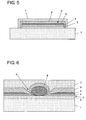
- FIG. 5 shows a cross sectional view of an organic EL device according to Embodiment 2 of the present invention.
- This organic EL device is such that a second sealing film 7 is formed on the surface of the sealing film 6 in Embodiment 1 shown in FIG. 1.
- An SiO 2 film having a thickness of 0.01 to 2.0 ⁇ m which is formed using polysilazane is used as the second sealing film 7.
- polysilazane contains dielectric as well in which a part of hydrogen atoms bonded to silicon atoms is replaced with an alkyl group or the like.
- the second sealing film 7 contains an alkyl group, especially, a methyl group having a small molecular weight, whereby the adhesive property with the sealing film 6 as a base is improved and the SiO 2 film is given flexibility, and hence even when a thickness of the second sealing film 7 is increased, the generation of cracks is suppressed.
- the alkyl group one having 1 to 4 carbon atoms is preferable.
- polysilazane may be one in a semidried state in which unreacted constituents are left therein.
- a method of manufacturing the organic EL device according to Embodiment 2 of the present invention will hereinafter be described.
- the anode 3, the organic light emitting layer 4, and the cathode 5 are successively laminated on the surface of the glass substrate 1 by utilizing the known thin film forming method such as the vapor deposition method to form the EL element 2.
- the glass substrate 1 having the EL element 2 formed thereon is conveyed to a position within a chamber of a plasma CVD system to form the sealing film 6 on the surface of the cathode 5 by supplying at least a SiH 4 gas and an N 2 gas into the chamber of the plasma CVD system and also at a deposition rate of equal to or higher than 300 nm/minute but equal to or lower than 600 nm/minute which is obtained by adjusting a flow rate of the SiH 4 gas and a supplied electric energy.
- the glass substrate 1 having the EL element 2 and the sealing film 6 formed thereon is exposed to the atmosphere to apply polysilazane onto the surface of the sealing film 6.
- the application method it is possible to utilize the various kinds of methods such as a spin coating method, a dip method, a flow method, a roll coating method, and a screen printing method.
- polysilazane may also be applied onto the surface of the sealing film 6 in the ambient atmosphere when the sealing film 6 was formed, or in the inactive ambient atmosphere without being exposed to the atmosphere.
- the glass substrate 1 having the EL element 2, the sealing film 6, and polysilazane formed thereon is subjected to the baking processing using a heating unit such as an oven or a hot plate so that the reaction in polysilazane proceeds in accordance with the following reaction formula to form the second sealing film 7 on the surface of the sealing film 6: [-SiH 2 NH-] n + 2H 2 O ⁇ SiO 2 + NH 3 + 2H 2
- the unadhered portion 9 can be covered with the second sealing film 7 to prevent the moisture and a gas from penetrating into the EL element 2.
- the unreacted constituent of the applied polisilazane in the process for the baking processing is left, the unreacted polysilazane reacts with the penetrated moisture, resulting in that the penetrated moisture is prevented from reaching the EL element 2. As a result, it is possible to prevent the degradation of the EL element 2 due to the penetrated moisture.
- Embodiments 1 and 2 of the present invention described above the description has been given with respect to a bottom emission type organic EL device in which the transparent anode 3, the organic light emitting layer 4, and the reflective cathode 5 are successively laminated on the glass substrate 1, and thus the light emitted from the organic light emitting layer 4 is transmitted through the transparent anode 3 and the glass substrate 1 to be emitted to the outside.
- the present invention is not intended to be limited to the bottom emission type organic EL device.
- the present invention is also applied to a top emission type organic EL device in which a reflective electrode, an organic light emitting layer, and a transparent electrode are successively laminated on a substrate, and thus light emitted from the organic light emitting layer is transmitted through the transparent electrode opposite to the substrate to be emitted to the outside.
- first and second sealing films are successively formed on the transparent electrode.
- each of the first and second sealing films must be made of a transparent or semitransparent material adapted to transmit the visible light.
- the sealing film made of Si and SiN x in which the ratio of the number of silicon atoms bonded to silicon atoms to the number of silicon atoms bonded to nitrogen atoms is equal to or larger than 0.6 but is equal to or smaller than 2.0 is formed on the surface of the EL element.
- An anode with 190 nm thickness made of ITO was formed on a transparent glass substrate by utilizing a reactive sputtering method. Then, as the cleaning for the substrate before the formation of a light emitting layer by the vapor deposition, the substrate was cleaned using an alkali solution, and was then cleaned using purified water, and after being dried, the substrate was cleaned using an ultraviolet light/ozone cleaning light source.
- the substrate having the anode formed thereon was transferred to a vapor deposition system, and copper phthalocyanine was then deposited in a thickness of 10 nm on the surface of the anode to form a hole injection region at a deposition rate of 0.1 nm/second and at a degree of vacuum of about 5. 0 x 10 -5 Pa using a carbon crucible.
- tetramer of a triphenylamine was deposited in a thickness of 30 nm on the surface of the hole injection region to form a hole transport region at a deposition rate of 0.1 nm/second and at a degree of vacuum of 5.0 x 10 -5 PA using a carbon crucible.
- DPVBi color of emitted light : blue
- DPVBi color of emitted light : blue
- Alq3 as a quinolinolato series metal complex was deposited in a thickness of 20 nm on the light emitting region to form an electron transport region at a deposition rate of 0.1 nm/second and at a degree of vacuum of about 5.0 x 10 -5 Pa using a carbon crucible.
- LiF was deposited in a thickness of 0.5 nm on the electron transport region to form a cathode interface region at a deposition rate of 0.03 nm/second and at a degree of vacuum of 5.0 x 10 -5 Pa using a carbon crucible.
- aluminum was deposited in a thickness of 100 nm on the cathode interface region to form a cathode at a deposition rate of 1 nm/second and at a degree of vacuum of about 5.0 x 10 -5 Pa using a tungsten board.
- a film made of Si and SiN x was formed as the sealing film on the surface of the EL element using a plasma CVD system. That is, the glass substrate was put into the chamber of the plasma CVD system, and air within the chamber was exhausted to a pressure of 1.0 x 10 -3 Pa. Then, a SiN 4 gas, an NH 3 gas, and an N 2 gas, were caused to flow into the chamber at a flow rate of 300 ml/minute, at a flow rate of 50 ml/minute, and at a flow rate of 1,000 ml/minute, respectively, to adjust a pressure to 100 Pa.
- a high frequency electric power of 13.56 MHz and 700 W was applied across a pair of electrodes having a gap of 20 mm to discharge the mixed gas, thereby depositing and forming the sealing film in a thickness of 1 ⁇ m on the surface of the EL element.
- a ratio of the number of silicon atoms bonded to silicon atoms to the number of silicon atoms bonded to nitrogen atoms in the sealing film of the organic EL device thus manufactured was 1.169. Also, when the water vapor permeability of the sealing film was measured, the water vapor permeability was equal to or lower than a limit in measurement precision. The amount of stress change after the formed sealing film was left under the environment in which a temperature was 60°C and a relative humidity was 90% for 500 hours was such a small value as to be -2.82 MPa.
- Example 2 Similarly to Example 1, after an EL element was formed on a transparent glass substrate and a sealing film made of Si and SiN x was formed on the surface of the EL element using a plasma CVD system, 20 wt% polysilazane, i.e., NL-120 (manufactured by CLARIANT JAPAN Co., Ltd.) was applied onto the surface of the sealing film using a spinner having a rotating speed set as 500 rpm to be dried at 90°C for 30 minutes using a hot plate, thereby forming a second sealing film made of SiO 2 a thickness of 0.5 ⁇ m.
- NL-120 manufactured by CLARIANT JAPAN Co., Ltd.
- An EL device including an anode, an organic light emitting layer, and a cathode is formed on a glass substrate, and a sealing film made of Si and SiN x in which a ratio of the number of silicon atoms bonded to silicon atoms to the number of silicon atoms bonded to nitrogen atoms is equal to or larger than 0.6 but is equal to or smaller than 2.0 is formed on a surface of the EL element so as to cover the EL element.
Landscapes
- Chemical & Material Sciences (AREA)
- Engineering & Computer Science (AREA)
- Optics & Photonics (AREA)
- Physics & Mathematics (AREA)
- Mechanical Engineering (AREA)
- Materials Engineering (AREA)
- Chemical Kinetics & Catalysis (AREA)
- Metallurgy (AREA)
- Organic Chemistry (AREA)
- General Chemical & Material Sciences (AREA)
- Inorganic Chemistry (AREA)
- Manufacturing & Machinery (AREA)
- Electroluminescent Light Sources (AREA)
- Chemical Vapour Deposition (AREA)
Applications Claiming Priority (2)
| Application Number | Priority Date | Filing Date | Title |
|---|---|---|---|
| JP2004100450 | 2004-03-30 | ||
| JP2004100450A JP2005285659A (ja) | 2004-03-30 | 2004-03-30 | 有機el装置及びその製造方法 |
Publications (1)
| Publication Number | Publication Date |
|---|---|
| EP1587153A1 true EP1587153A1 (de) | 2005-10-19 |
Family
ID=34933763
Family Applications (1)
| Application Number | Title | Priority Date | Filing Date |
|---|---|---|---|
| EP05003184A Withdrawn EP1587153A1 (de) | 2004-03-30 | 2005-02-15 | Organische EL-Vorrichtung und deren Herstellungsverfahren |
Country Status (6)
| Country | Link |
|---|---|
| US (1) | US20050218803A1 (de) |
| EP (1) | EP1587153A1 (de) |
| JP (1) | JP2005285659A (de) |
| KR (1) | KR100656137B1 (de) |
| CN (2) | CN100433403C (de) |
| TW (1) | TWI270313B (de) |
Cited By (1)
| Publication number | Priority date | Publication date | Assignee | Title |
|---|---|---|---|---|
| EP2085495A3 (de) * | 2008-02-01 | 2010-12-01 | FUJIFILM Corporation | Ablagerungsverfahren für eine Gassperrschicht, Gassperrfolie und organische Vorrichtung |
Families Citing this family (21)
| Publication number | Priority date | Publication date | Assignee | Title |
|---|---|---|---|---|
| US20070040501A1 (en) * | 2005-08-18 | 2007-02-22 | Aitken Bruce G | Method for inhibiting oxygen and moisture degradation of a device and the resulting device |
| US20070120108A1 (en) * | 2005-11-30 | 2007-05-31 | Alps Electric Co., Ltd. | Light emitting device |
| JP2007184251A (ja) * | 2005-12-07 | 2007-07-19 | Sony Corp | 表示装置 |
| JP2007173084A (ja) * | 2005-12-22 | 2007-07-05 | Canon Inc | 発光素子 |
| JP4809186B2 (ja) * | 2006-10-26 | 2011-11-09 | 京セラ株式会社 | 有機elディスプレイおよびその製造方法 |
| KR20110040616A (ko) | 2008-07-24 | 2011-04-20 | 후지 덴키 홀딩스 가부시키가이샤 | 유기 el 디바이스 및 그 제조 방법 |
| CN102084716B (zh) | 2008-08-26 | 2014-05-14 | 夏普株式会社 | 有机el器件及其制造方法 |
| JP5405075B2 (ja) * | 2008-09-24 | 2014-02-05 | 富士フイルム株式会社 | ガスバリア膜の形成方法およびガスバリア膜 |
| KR101718560B1 (ko) * | 2009-04-09 | 2017-03-21 | 스미또모 가가꾸 가부시키가이샤 | 가스 배리어성 적층 필름 |
| JP2010260347A (ja) * | 2009-04-09 | 2010-11-18 | Sumitomo Chemical Co Ltd | ガスバリア性積層フィルム |
| JP5513959B2 (ja) * | 2009-09-01 | 2014-06-04 | 住友化学株式会社 | ガスバリア性積層フィルム |
| KR101347471B1 (ko) | 2009-09-29 | 2014-01-02 | 샤프 가부시키가이샤 | 유기 el 디바이스 및 유기 el 디바이스의 제조 방법 |
| JP5375732B2 (ja) * | 2010-04-26 | 2013-12-25 | 株式会社島津製作所 | バリヤ膜を形成する方法およびバリヤ膜を形成するために用いるcvd装置 |
| WO2014017183A1 (ja) * | 2012-07-24 | 2014-01-30 | 三井金属鉱業株式会社 | 電極箔及び有機発光デバイス |
| US9373815B2 (en) | 2012-09-10 | 2016-06-21 | Kaneka Corporation | Sealing layer of organic EL device |
| CN104995716B (zh) * | 2012-12-31 | 2018-05-11 | 美国圣戈班性能塑料公司 | 柔性基材上的薄膜氮化硅阻挡层 |
| CN103910885A (zh) | 2012-12-31 | 2014-07-09 | 第一毛织株式会社 | 制备间隙填充剂的方法、用其制备的间隙填充剂和使用间隙填充剂制造半导体电容器的方法 |
| JP6515537B2 (ja) | 2014-04-08 | 2019-05-22 | セイコーエプソン株式会社 | 有機el装置の製造方法、有機el装置、電子機器 |
| CN104051671B (zh) | 2014-06-16 | 2016-03-16 | 京东方科技集团股份有限公司 | 一种oled显示装置及其制备方法 |
| JP6613196B2 (ja) | 2016-03-31 | 2019-11-27 | 株式会社Joled | 有機el表示パネル |
| JP6455481B2 (ja) * | 2016-04-25 | 2019-01-23 | トヨタ自動車株式会社 | 成膜方法及び成膜装置 |
Citations (4)
| Publication number | Priority date | Publication date | Assignee | Title |
|---|---|---|---|---|
| US5072263A (en) * | 1986-09-19 | 1991-12-10 | Kabushiki Kaisha Komatsu Seisakusho | Thin film el device with protective film |
| US20020070663A1 (en) * | 2000-10-03 | 2002-06-13 | Keiiti Ogura | Light emitting device |
| JP2003118030A (ja) | 2001-10-16 | 2003-04-23 | Asahi Glass Co Ltd | ガスバリヤ性有機基材およびそれを用いたエレクトロルミネッセンス素子 |
| US20030164677A1 (en) | 1999-01-29 | 2003-09-04 | Satoshi Miyaguchi | Organic electroluminescence (El) cell and a method for producing the same |
Family Cites Families (9)
| Publication number | Priority date | Publication date | Assignee | Title |
|---|---|---|---|---|
| US164677A (en) * | 1875-06-22 | Improvement in mail-bag catches | ||
| US70663A (en) * | 1867-11-05 | wilder | ||
| JPH07335753A (ja) * | 1994-06-06 | 1995-12-22 | Sharp Corp | 半導体装置及びその製造方法 |
| CN2240185Y (zh) * | 1995-07-04 | 1996-11-13 | 张志林 | 硬密封的电致发光塑料屏 |
| US6552488B1 (en) * | 1999-08-24 | 2003-04-22 | Agilent Technologies, Inc. | Organic electroluminescent device |
| JP4556282B2 (ja) * | 2000-03-31 | 2010-10-06 | 株式会社デンソー | 有機el素子およびその製造方法 |
| KR100413450B1 (ko) * | 2001-07-20 | 2003-12-31 | 엘지전자 주식회사 | 표시소자의 보호막 구조 |
| JP3705264B2 (ja) * | 2001-12-18 | 2005-10-12 | セイコーエプソン株式会社 | 表示装置及び電子機器 |
| US6743524B2 (en) * | 2002-05-23 | 2004-06-01 | General Electric Company | Barrier layer for an article and method of making said barrier layer by expanding thermal plasma |
-
2004
- 2004-03-30 JP JP2004100450A patent/JP2005285659A/ja active Pending
-
2005
- 2005-02-10 US US11/055,311 patent/US20050218803A1/en not_active Abandoned
- 2005-02-15 EP EP05003184A patent/EP1587153A1/de not_active Withdrawn
- 2005-02-21 TW TW094104979A patent/TWI270313B/zh not_active IP Right Cessation
- 2005-02-28 CN CNB2005100524690A patent/CN100433403C/zh not_active Expired - Fee Related
- 2005-02-28 CN CNA2008101490619A patent/CN101369637A/zh active Pending
- 2005-03-29 KR KR1020050026229A patent/KR100656137B1/ko not_active Expired - Fee Related
Patent Citations (4)
| Publication number | Priority date | Publication date | Assignee | Title |
|---|---|---|---|---|
| US5072263A (en) * | 1986-09-19 | 1991-12-10 | Kabushiki Kaisha Komatsu Seisakusho | Thin film el device with protective film |
| US20030164677A1 (en) | 1999-01-29 | 2003-09-04 | Satoshi Miyaguchi | Organic electroluminescence (El) cell and a method for producing the same |
| US20020070663A1 (en) * | 2000-10-03 | 2002-06-13 | Keiiti Ogura | Light emitting device |
| JP2003118030A (ja) | 2001-10-16 | 2003-04-23 | Asahi Glass Co Ltd | ガスバリヤ性有機基材およびそれを用いたエレクトロルミネッセンス素子 |
Cited By (1)
| Publication number | Priority date | Publication date | Assignee | Title |
|---|---|---|---|---|
| EP2085495A3 (de) * | 2008-02-01 | 2010-12-01 | FUJIFILM Corporation | Ablagerungsverfahren für eine Gassperrschicht, Gassperrfolie und organische Vorrichtung |
Also Published As
| Publication number | Publication date |
|---|---|
| CN1678151A (zh) | 2005-10-05 |
| CN100433403C (zh) | 2008-11-12 |
| KR20060044954A (ko) | 2006-05-16 |
| TWI270313B (en) | 2007-01-01 |
| US20050218803A1 (en) | 2005-10-06 |
| CN101369637A (zh) | 2009-02-18 |
| KR100656137B1 (ko) | 2006-12-13 |
| JP2005285659A (ja) | 2005-10-13 |
| TW200539734A (en) | 2005-12-01 |
Similar Documents
| Publication | Publication Date | Title |
|---|---|---|
| EP1587153A1 (de) | Organische EL-Vorrichtung und deren Herstellungsverfahren | |
| US7170087B2 (en) | EL device and method for manufacturing the same | |
| KR101061880B1 (ko) | 발광장치 및 전자 기기, 및 제조 장치 | |
| US8638032B2 (en) | Organic optoelectronic device coated with a multilayer encapsulation structure and a method for encapsulating said device | |
| US7648925B2 (en) | Multilayer barrier stacks and methods of making multilayer barrier stacks | |
| US6660409B1 (en) | Electronic device and process for producing the same | |
| US6933002B2 (en) | Method for manufacturing organic EL device with protective layer | |
| US20160056414A1 (en) | Thin film permeation barrier system for substrates and devices and method of making the same | |
| JP5241173B2 (ja) | 有機el素子の製造方法 | |
| JP2008153004A (ja) | 有機エレクトロルミネッセンス素子 | |
| US20160254487A1 (en) | Permeation barrier system for substrates and devices and method of making the same | |
| CN1961095B (zh) | 用以沉积低温无机层至大型塑胶基板上的方法及其设备 | |
| JP2005527076A (ja) | 有機電気光学素子の気密封止 | |
| US8299706B2 (en) | Hermetic encapsulation of organic, electro-optical elements | |
| JP2005166400A (ja) | 表面保護膜 | |
| US9472783B2 (en) | Barrier coating with reduced process time | |
| KR100942038B1 (ko) | 유기 광전 소자 및 유기 광전 소자 제조 방법 | |
| JP2000077183A (ja) | 有機エレクトロルミネセンス素子の製造方法 | |
| WO2015061656A1 (en) | Flexible permation barrier system deposited in a single process and having ultralow permeability and low mechanical stress over its service life | |
| Eritt et al. | 46.4: Up‐Scaling of OLED Manufacturing for Lighting Applications |
Legal Events
| Date | Code | Title | Description |
|---|---|---|---|
| PUAI | Public reference made under article 153(3) epc to a published international application that has entered the european phase |
Free format text: ORIGINAL CODE: 0009012 |
|
| 17P | Request for examination filed |
Effective date: 20050215 |
|
| AK | Designated contracting states |
Kind code of ref document: A1 Designated state(s): AT BE BG CH CY CZ DE DK EE ES FI FR GB GR HU IE IS IT LI LT LU MC NL PL PT RO SE SI SK TR |
|
| AX | Request for extension of the european patent |
Extension state: AL BA HR LV MK YU |
|
| AKX | Designation fees paid |
Designated state(s): DE FI GB NL |
|
| STAA | Information on the status of an ep patent application or granted ep patent |
Free format text: STATUS: THE APPLICATION IS DEEMED TO BE WITHDRAWN |
|
| 18D | Application deemed to be withdrawn |
Effective date: 20120830 |