EP1587140B1 - Dispositif électronique qui contient un circuit électronique pourvu d'une couche de gel et procédé de fabrication de ce dispositif - Google Patents
Dispositif électronique qui contient un circuit électronique pourvu d'une couche de gel et procédé de fabrication de ce dispositif Download PDFInfo
- Publication number
- EP1587140B1 EP1587140B1 EP05101527A EP05101527A EP1587140B1 EP 1587140 B1 EP1587140 B1 EP 1587140B1 EP 05101527 A EP05101527 A EP 05101527A EP 05101527 A EP05101527 A EP 05101527A EP 1587140 B1 EP1587140 B1 EP 1587140B1
- Authority
- EP
- European Patent Office
- Prior art keywords
- gel
- gel layer
- substrate
- layer
- hardness
- Prior art date
- Legal status (The legal status is an assumption and is not a legal conclusion. Google has not performed a legal analysis and makes no representation as to the accuracy of the status listed.)
- Not-in-force
Links
- 238000004519 manufacturing process Methods 0.000 title claims description 5
- 239000000758 substrate Substances 0.000 claims description 25
- -1 polydimethylsiloxane Polymers 0.000 claims description 15
- 239000004848 polyfunctional curative Substances 0.000 claims description 8
- 229920000435 poly(dimethylsiloxane) Polymers 0.000 claims description 6
- 239000002318 adhesion promoter Substances 0.000 claims description 5
- 239000004205 dimethyl polysiloxane Substances 0.000 claims description 5
- 238000000034 method Methods 0.000 claims description 5
- 125000003545 alkoxy group Chemical group 0.000 claims description 4
- 229920001296 polysiloxane Polymers 0.000 claims description 4
- 239000003822 epoxy resin Substances 0.000 claims description 3
- 229920000647 polyepoxide Polymers 0.000 claims description 3
- 239000010695 polyglycol Substances 0.000 claims description 3
- 229920000151 polyglycol Polymers 0.000 claims description 3
- 229920002635 polyurethane Polymers 0.000 claims description 3
- 239000004814 polyurethane Substances 0.000 claims description 3
- 239000000499 gel Substances 0.000 description 64
- 230000007797 corrosion Effects 0.000 description 6
- 238000005260 corrosion Methods 0.000 description 6
- VYPSYNLAJGMNEJ-UHFFFAOYSA-N Silicium dioxide Chemical compound O=[Si]=O VYPSYNLAJGMNEJ-UHFFFAOYSA-N 0.000 description 5
- 150000001875 compounds Chemical class 0.000 description 4
- 239000000463 material Substances 0.000 description 4
- 238000005259 measurement Methods 0.000 description 4
- 229920002554 vinyl polymer Polymers 0.000 description 4
- 239000003795 chemical substances by application Substances 0.000 description 3
- 238000000576 coating method Methods 0.000 description 3
- 235000013870 dimethyl polysiloxane Nutrition 0.000 description 3
- 230000035515 penetration Effects 0.000 description 3
- 230000001133 acceleration Effects 0.000 description 2
- 229920005601 base polymer Polymers 0.000 description 2
- 230000001588 bifunctional effect Effects 0.000 description 2
- 239000007767 bonding agent Substances 0.000 description 2
- KPUWHANPEXNPJT-UHFFFAOYSA-N disiloxane Chemical class [SiH3]O[SiH3] KPUWHANPEXNPJT-UHFFFAOYSA-N 0.000 description 2
- 230000000694 effects Effects 0.000 description 2
- 230000007613 environmental effect Effects 0.000 description 2
- BASFCYQUMIYNBI-UHFFFAOYSA-N platinum Substances [Pt] BASFCYQUMIYNBI-UHFFFAOYSA-N 0.000 description 2
- 238000012545 processing Methods 0.000 description 2
- 239000000377 silicon dioxide Substances 0.000 description 2
- 238000012360 testing method Methods 0.000 description 2
- 238000005382 thermal cycling Methods 0.000 description 2
- 125000000391 vinyl group Chemical group [H]C([*])=C([H])[H] 0.000 description 2
- PNEYBMLMFCGWSK-UHFFFAOYSA-N Alumina Chemical class [O-2].[O-2].[O-2].[Al+3].[Al+3] PNEYBMLMFCGWSK-UHFFFAOYSA-N 0.000 description 1
- CPELXLSAUQHCOX-UHFFFAOYSA-M Bromide Chemical compound [Br-] CPELXLSAUQHCOX-UHFFFAOYSA-M 0.000 description 1
- VEXZGXHMUGYJMC-UHFFFAOYSA-M Chloride anion Chemical compound [Cl-] VEXZGXHMUGYJMC-UHFFFAOYSA-M 0.000 description 1
- DGAQECJNVWCQMB-PUAWFVPOSA-M Ilexoside XXIX Chemical compound C[C@@H]1CC[C@@]2(CC[C@@]3(C(=CC[C@H]4[C@]3(CC[C@@H]5[C@@]4(CC[C@@H](C5(C)C)OS(=O)(=O)[O-])C)C)[C@@H]2[C@]1(C)O)C)C(=O)O[C@H]6[C@@H]([C@H]([C@@H]([C@H](O6)CO)O)O)O.[Na+] DGAQECJNVWCQMB-PUAWFVPOSA-M 0.000 description 1
- WHXSMMKQMYFTQS-UHFFFAOYSA-N Lithium Chemical compound [Li] WHXSMMKQMYFTQS-UHFFFAOYSA-N 0.000 description 1
- ZLMJMSJWJFRBEC-UHFFFAOYSA-N Potassium Chemical compound [K] ZLMJMSJWJFRBEC-UHFFFAOYSA-N 0.000 description 1
- BLRPTPMANUNPDV-UHFFFAOYSA-N Silane Chemical compound [SiH4] BLRPTPMANUNPDV-UHFFFAOYSA-N 0.000 description 1
- FAPWRFPIFSIZLT-UHFFFAOYSA-M Sodium chloride Chemical compound [Na+].[Cl-] FAPWRFPIFSIZLT-UHFFFAOYSA-M 0.000 description 1
- 230000002528 anti-freeze Effects 0.000 description 1
- 238000005266 casting Methods 0.000 description 1
- 239000003054 catalyst Substances 0.000 description 1
- 229910010293 ceramic material Inorganic materials 0.000 description 1
- 239000011248 coating agent Substances 0.000 description 1
- 230000001419 dependent effect Effects 0.000 description 1
- 238000001514 detection method Methods 0.000 description 1
- 238000011161 development Methods 0.000 description 1
- 230000018109 developmental process Effects 0.000 description 1
- 238000011156 evaluation Methods 0.000 description 1
- 239000000945 filler Substances 0.000 description 1
- LNEPOXFFQSENCJ-UHFFFAOYSA-N haloperidol Chemical compound C1CC(O)(C=2C=CC(Cl)=CC=2)CCN1CCCC(=O)C1=CC=C(F)C=C1 LNEPOXFFQSENCJ-UHFFFAOYSA-N 0.000 description 1
- 238000007542 hardness measurement Methods 0.000 description 1
- 150000004678 hydrides Chemical class 0.000 description 1
- 238000006459 hydrosilylation reaction Methods 0.000 description 1
- 239000003112 inhibitor Substances 0.000 description 1
- 238000011835 investigation Methods 0.000 description 1
- 229910052744 lithium Inorganic materials 0.000 description 1
- 239000007769 metal material Substances 0.000 description 1
- 239000000203 mixture Substances 0.000 description 1
- 239000003921 oil Substances 0.000 description 1
- 150000002902 organometallic compounds Chemical class 0.000 description 1
- 229910052574 oxide ceramic Inorganic materials 0.000 description 1
- 239000011224 oxide ceramic Substances 0.000 description 1
- TWNQGVIAIRXVLR-UHFFFAOYSA-N oxo(oxoalumanyloxy)alumane Chemical compound O=[Al]O[Al]=O TWNQGVIAIRXVLR-UHFFFAOYSA-N 0.000 description 1
- 239000004033 plastic Substances 0.000 description 1
- 229920003023 plastic Polymers 0.000 description 1
- 229910052697 platinum Inorganic materials 0.000 description 1
- 229910052700 potassium Inorganic materials 0.000 description 1
- 239000011591 potassium Substances 0.000 description 1
- 230000001681 protective effect Effects 0.000 description 1
- 238000000926 separation method Methods 0.000 description 1
- 229910000077 silane Inorganic materials 0.000 description 1
- 150000004756 silanes Chemical class 0.000 description 1
- 239000000741 silica gel Substances 0.000 description 1
- 229910002027 silica gel Inorganic materials 0.000 description 1
- 235000012239 silicon dioxide Nutrition 0.000 description 1
- 229910052708 sodium Inorganic materials 0.000 description 1
- 239000011734 sodium Substances 0.000 description 1
- 239000011780 sodium chloride Substances 0.000 description 1
- 239000011550 stock solution Substances 0.000 description 1
- 239000013008 thixotropic agent Substances 0.000 description 1
Images
Classifications
-
- H—ELECTRICITY
- H01—ELECTRIC ELEMENTS
- H01L—SEMICONDUCTOR DEVICES NOT COVERED BY CLASS H10
- H01L23/00—Details of semiconductor or other solid state devices
- H01L23/16—Fillings or auxiliary members in containers or encapsulations, e.g. centering rings
- H01L23/18—Fillings characterised by the material, its physical or chemical properties, or its arrangement within the complete device
- H01L23/24—Fillings characterised by the material, its physical or chemical properties, or its arrangement within the complete device solid or gel at the normal operating temperature of the device
-
- H—ELECTRICITY
- H02—GENERATION; CONVERSION OR DISTRIBUTION OF ELECTRIC POWER
- H02K—DYNAMO-ELECTRIC MACHINES
- H02K11/00—Structural association of dynamo-electric machines with electric components or with devices for shielding, monitoring or protection
- H02K11/20—Structural association of dynamo-electric machines with electric components or with devices for shielding, monitoring or protection for measuring, monitoring, testing, protecting or switching
-
- H—ELECTRICITY
- H02—GENERATION; CONVERSION OR DISTRIBUTION OF ELECTRIC POWER
- H02K—DYNAMO-ELECTRIC MACHINES
- H02K11/00—Structural association of dynamo-electric machines with electric components or with devices for shielding, monitoring or protection
- H02K11/30—Structural association with control circuits or drive circuits
- H02K11/33—Drive circuits, e.g. power electronics
-
- H—ELECTRICITY
- H02—GENERATION; CONVERSION OR DISTRIBUTION OF ELECTRIC POWER
- H02K—DYNAMO-ELECTRIC MACHINES
- H02K19/00—Synchronous motors or generators
- H02K19/16—Synchronous generators
- H02K19/36—Structural association of synchronous generators with auxiliary electric devices influencing the characteristic of the generator or controlling the generator, e.g. with impedances or switches
- H02K19/365—Structural association of synchronous generators with auxiliary electric devices influencing the characteristic of the generator or controlling the generator, e.g. with impedances or switches with a voltage regulator
-
- H—ELECTRICITY
- H01—ELECTRIC ELEMENTS
- H01L—SEMICONDUCTOR DEVICES NOT COVERED BY CLASS H10
- H01L2224/00—Indexing scheme for arrangements for connecting or disconnecting semiconductor or solid-state bodies and methods related thereto as covered by H01L24/00
- H01L2224/01—Means for bonding being attached to, or being formed on, the surface to be connected, e.g. chip-to-package, die-attach, "first-level" interconnects; Manufacturing methods related thereto
- H01L2224/42—Wire connectors; Manufacturing methods related thereto
- H01L2224/47—Structure, shape, material or disposition of the wire connectors after the connecting process
- H01L2224/48—Structure, shape, material or disposition of the wire connectors after the connecting process of an individual wire connector
- H01L2224/4805—Shape
- H01L2224/4809—Loop shape
- H01L2224/48091—Arched
-
- H—ELECTRICITY
- H01—ELECTRIC ELEMENTS
- H01L—SEMICONDUCTOR DEVICES NOT COVERED BY CLASS H10
- H01L2224/00—Indexing scheme for arrangements for connecting or disconnecting semiconductor or solid-state bodies and methods related thereto as covered by H01L24/00
- H01L2224/01—Means for bonding being attached to, or being formed on, the surface to be connected, e.g. chip-to-package, die-attach, "first-level" interconnects; Manufacturing methods related thereto
- H01L2224/42—Wire connectors; Manufacturing methods related thereto
- H01L2224/47—Structure, shape, material or disposition of the wire connectors after the connecting process
- H01L2224/48—Structure, shape, material or disposition of the wire connectors after the connecting process of an individual wire connector
- H01L2224/481—Disposition
- H01L2224/48135—Connecting between different semiconductor or solid-state bodies, i.e. chip-to-chip
- H01L2224/48137—Connecting between different semiconductor or solid-state bodies, i.e. chip-to-chip the bodies being arranged next to each other, e.g. on a common substrate
-
- H—ELECTRICITY
- H01—ELECTRIC ELEMENTS
- H01L—SEMICONDUCTOR DEVICES NOT COVERED BY CLASS H10
- H01L2224/00—Indexing scheme for arrangements for connecting or disconnecting semiconductor or solid-state bodies and methods related thereto as covered by H01L24/00
- H01L2224/73—Means for bonding being of different types provided for in two or more of groups H01L2224/10, H01L2224/18, H01L2224/26, H01L2224/34, H01L2224/42, H01L2224/50, H01L2224/63, H01L2224/71
- H01L2224/732—Location after the connecting process
- H01L2224/73251—Location after the connecting process on different surfaces
- H01L2224/73265—Layer and wire connectors
Definitions
- the invention relates to an electronic component and a method for its production and its use according to the preamble of the independent claims.
- Gel systems the hardness of which is assigned to this hardness range, tend with shaking loads to strong gel movements, which damage the electronics to be protected (chips, bonding wires) and leads to so-called heel breaks especially with bonding wires.
- such gel systems show unsatisfactory hardness stabilities in the event of high-temperature stresses.
- components with soft gels whose hardness is in the penetration range, can not be completely covered with gel or only coated with a relatively thin layer of gel. They remain vulnerable to corrosive media.
- Object of the present invention is to provide an electronic component, which has a cost effective and effective protection against environmental influences, even with temperature or Scblinbelastept.
- the component according to the invention or the method for its production according to the characterizing features of the independent claims has the advantage over the prior art that corrosion-sensitive areas of the component are sealed with a suitable gel coating in such a way that an influence of weathering on the protected areas is prevented and this protective effect is maintained even at high thermal and mechanical loads.
- This is achieved by the component according to the invention comprises a gel layer whose Shore00 hardness is located in a range in which the gel on the one hand shows no plastic deformation under mechanical influences, on the other hand, however, is not so brittle that Scblinbelastened the component to cracks or Lead to separation phenomena. This is the case in particular in a Shore00 hardness range of 40 to 48 points.
- the component provided with the gel layer satisfies both high dynamic requirements and thermal cycling as well as high-temperature or low-temperature stresses, without the corrosion protection for corrosion-sensitive components of the component being lost.
- the gel hardness in a medium hardness range, a relatively rigid, three-dimensional network is obtained, which in contrast to dynamic loads, such as in the case of The use of electronic controller components for generators, reacting unresponsive and avoid bonding wire breakages in bonding wires with a diameter of over 50 microns.
- the gel is still insensitive to commonly occurring in the engine compartment media such. As oils, antifreeze, gasoline, diesel, cold cleaners or saline deposits.
- the gel layer is based on a polydimethylsiloxane, a polyurethane or an epoxy resin, since these materials are particularly robust and resistant to media.
- gel systems based on vinyl group-modified polydimethylsiloxanes are especially suitable.
- Another particular advantage of the claimed gel layer is that even greater layer thicknesses of the gel layer of more than 3 ⁇ m can be realized without cracks or detachment phenomena occurring in continuous operation.
- a layer of an adhesion promoter is provided between the substrate and the gel layer, so that a particularly stable attachment of the gel layer to the substrate to be protected is achieved.
- the primer layer is based on an alkylvinylsiloxane having glycidoxy or alkoxy termination, a bifunctional silane such as a glycidoxyalkyltrialkoxysilane or a silylated polyglycol.
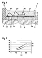
- FIG. 1 a cross section through an inventive component, the corrosion-sensitive areas are protected with a gel layer
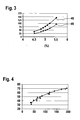
- FIG. 2 a correlation between the concentration of the hardener in the gel in% by weight and the resulting Shore00 hardness of the cured gel as a function of the processing temperature
- FIG. 3 a correlation between the concentration of the hardener in the Gel in% by weight and the force to be used in a measurement of the cured gel with a texture analyzer depending on the processing temperature
- FIG. 4 a correlation of the force determined by a texture analyzer and the corresponding Shore00 hardness of the gel.
- FIG. 1 an inventive electronic component in the form of a regulator 10 according to a first embodiment of the present invention is shown.
- the controller 10 comprises a substrate 12, which is made for example of a ceramic material or of a suitable polymeric material such as PET.
- the substrate 12 is arranged on a heat sink 14, which serves to dissipate heat energy arising and is made of a suitable, for example, metallic material.
- the heat sink 14 is in contact with a housing 16, which simultaneously acts as a boundary of the substrate 12.
- the substrate 12 is part of the housing 16.
- a heat-conducting layer 18 is provided, on which a circuit 20, preferably an integrated circuit is located.
- a circuit 20 preferably an integrated circuit is located.
- contact tracks 22a, 22b are further provided, which serve the electrical contacting of the electronic components of the component 10.
- the micromechanical sensor element may, for example, be designed as a pressure sensor.
- the circuit 20 and the additional substrate 24 are contacted with each other, for example, by a first bonding wire 26a.
- the additional substrate 24 is electrically contacted via a second bonding wire 26b to the contact track 22a.
- the circuit 20 is also connected to the contact track 22b by a third bonding wire 26c.
- the circuit 20 serves, for example, for controlling, measured value detection and evaluation of the electronic component in the form of the additional substrate 24.
- the component 10 furthermore has a gel layer 28 which covers the substrate 12 on its side facing away from the heat sink 14 at least in regions.
- the gel layer 28 is bounded laterally by the housing 16 and an overflow 30 spatially in its extension.
- the layer thickness of the gel is preferably dimensioned so that all corrosion-sensitive electronic components such as the circuit 20 and the additional substrate 24 are enclosed by the gel layer 28.
- the gel layer 28 is preferably made on the basis of a vinyl-modified polydimethylsiloxane.
- the gel layer 28 is preferably produced in such a way that a gel based on a suitable polysiloxane is introduced into the cavity formed by the housing 16, the substrate 12 and the overflow 30.
- the gel further contains a suitable curing agent based on a polysiloxane having terminal and optionally further hydride groups.
- the gel may, for example, be designed as a two-component system and have the following exemplary composition: Component A - Vinyl-containing base polymer about 98-99% by weight - bonding agent about 1% by weight - platinum catalyst (organometallic compound) about 0.5% by weight of a Pt-containing stock solution - Inhibitor ⁇ 1% by weight Component B - Vinyl-containing base polymer approx. 84 - 94 wt.% - bonding agent about 1% by weight - Harder about 5 - 15 wt.%
- the gel may further contain fillers, such as finely divided silica as a thixotropic agent or silica gel or aluminum oxides.
- the gel layer 28 Since the gel layer 28 is in direct contact with electronic components, the gel must have high ionic purity, particularly with respect to its potassium, sodium, lithium, chloride or bromide content, to avoid contact corrosion and associated electrical faults.
- the gel is crosslinked at temperatures of 120 to 180 ° C in an oven via a platinum-catalyzed hydrosilylation reaction.
- the concentration of the hardener in the gel is selected so that the resulting gel layer 28 after curing has a Shore00 hardness of 30 to 50, preferably from 40 to 48 points.
- FIG. 2 shows a plot of the achievable Shore00 hardness of the cured gel over the concentration of hardener contained in the gel in wt.%
- the gel hardness measurement via the Texture Analyzer measures the force required to allow a specimen to penetrate a certain distance into the sample to be examined.
- This type of measurement of the so-called texture of the specimen is used primarily in the food industry and responds to differences in specimens such as e.g. Layer thickness variances, shape and material as well as influences due to wall or floor effects of the measuring tank are very sensitive. For the comparability of the measurements, therefore, the same test specimens with a uniform layer thickness (ie filling quantity) must be used.
- curve 46 shows, analogous to curve 40, the achievable hardness if the curing of the gel is carried out for one hour at 120 ° C. and curve 48 is analogous to curve 42 the achievable hardness when the gel is cured for two hours at a temperature of 150 ° C.
- FIG. 4 shows a correlation of hardness values obtained via a texture analyzer with the corresponding Shore00 hardness.
- the gel used contains an adhesion promoter, suitable compounds being, in particular, compounds which on the one hand have an alkoxy group and, on the other hand, vinyl or Si-H groups, so that they have the necessary bifunctional character to be firmly bound both in the three-dimensional polymeric siloxane network of the gel layer 28 and at the same time have a good adhesion with the materials of the substrate 12 and the housing 16 or the overflow 30.
- suitable compounds being, in particular, compounds which on the one hand have an alkoxy group and, on the other hand, vinyl or Si-H groups, so that they have the necessary bifunctional character to be firmly bound both in the three-dimensional polymeric siloxane network of the gel layer 28 and at the same time have a good adhesion with the materials of the substrate 12 and the housing 16 or the overflow 30.
- alkylvinylsiloxanes or silanes with glycidoxy or alkoxy termination, glycidoxypropyltrialkoxysilanes, silylated polyglycols or derivatives of these compounds are suitable as adhesion promoters.
- the substrate 12 may be provided with a primer layer 32 prior to application of the gel layer 28.
- the gel layer 28 produced in this way is suitable for use temperatures between -45 and 150 degrees Celsius and also withstands dynamic loads, such as, for example, a sine-shaker test in the frequency range from 100 to 1000 Hz with an amplitude of 0.19 mm and a maximum acceleration of 300 m / s 2 occur as well as the loads in so-called random-vibration investigations with a maximum acceleration of up to 800 m / s 2 .
- dynamic loads such as, for example, a sine-shaker test in the frequency range from 100 to 1000 Hz with an amplitude of 0.19 mm and a maximum acceleration of 300 m / s 2 occur as well as the loads in so-called random-vibration investigations with a maximum acceleration of up to 800 m / s 2 .
Landscapes
- Engineering & Computer Science (AREA)
- Power Engineering (AREA)
- Microelectronics & Electronic Packaging (AREA)
- Chemical & Material Sciences (AREA)
- Dispersion Chemistry (AREA)
- Physics & Mathematics (AREA)
- Condensed Matter Physics & Semiconductors (AREA)
- General Physics & Mathematics (AREA)
- Computer Hardware Design (AREA)
- Structures Or Materials For Encapsulating Or Coating Semiconductor Devices Or Solid State Devices (AREA)
- Non-Metallic Protective Coatings For Printed Circuits (AREA)
- Micromachines (AREA)
Claims (10)
- Dispositif électronique, en particulier régulateur ou élément détecteur micromécanique, comportant un substrat et un boîtier entourant le substrat ainsi qu'un circuit disposé sur le substrat, dans lequel au moins le circuit est pourvu d'une couche de gel pour la protection contre les influences ambiantes, dans lequel la couche de gel (28) présente une dureté Shore 00 de 30 à 50 points, et dans lequel le gel de la couche de gel (28) contient un agent adhésif.
- Dispositif selon la revendication 1, caractérisé en ce que la couche de gel (28) présente une dureté Shore 00 de 40 à 48 points.
- Dispositif selon la revendication 1 ou 2, caractérisé en ce que la couche de gel (28) est réalisée à base d'un polydiméthylsiloxane, d'un polyuréthane ou d'une résine époxy.
- Dispositif selon la revendication 3, caractérisé en ce que la couche de gel (28) est réalisée à base d'un polydiméthylsiloxane modifié par un groupe vinyle.
- Dispositif selon l'une quelconque des revendications précédentes, caractérisé en ce que la couche de gel (28) présente une épaisseur de couche de plus de 3 µm.
- Dispositif selon la revendication 1, caractérisé en ce que l'agent adhésif est un alkylvinylsiloxane à terminaison glycidoxy ou alcoxy, un glycidoxyalkyltrialcoxysilane ou un polyglycol silylé.
- Procédé de fabrication d'un dispositif électronique ou électrique, en particulier d'un régulateur ou d'un élément détecteur micromécanique, comportant un substrat et un boîtier entourant le substrat ainsi qu'un circuit disposé sur le substrat, dans lequel on munit au moins le circuit d'une couche de gel pour la protection contre les influences ambiantes, dans lequel on règle la dureté Shore 00 de la couche de gel à une valeur de 30 à 50 points par la quantité d'un durcisseur ajoutée au gel, et dans lequel le gel de la couche de gel (28) contient un agent adhésif.
- Procédé selon la revendication 7, caractérisé en ce que l'on utilise comme gel un gel à base d'un polydiméthylsiloxane et comme durcisseur un polysiloxane hydruré.
- Procédé selon la revendication 7 ou 8, caractérisé en ce que l'on ajoute le durcisseur en une concentration de 4,2 à 5,7 % en poids du gel de la couche de gel.
- Utilisation d'un dispositif selon l'une quelconque des revendications 1 à 6 comme régulateur pour des générateurs ou comme détecteur de pression micromécanique dans des applications de véhicule automobile.
Applications Claiming Priority (4)
| Application Number | Priority Date | Filing Date | Title |
|---|---|---|---|
| DE102004012600 | 2004-03-12 | ||
| DE102004012600 | 2004-03-12 | ||
| DE102004028888 | 2004-06-15 | ||
| DE102004028888A DE102004028888A1 (de) | 2004-03-12 | 2004-06-15 | Elektronisches Bauteil und Verfahren zur Herstellung desselben |
Publications (3)
| Publication Number | Publication Date |
|---|---|
| EP1587140A2 EP1587140A2 (fr) | 2005-10-19 |
| EP1587140A3 EP1587140A3 (fr) | 2009-04-01 |
| EP1587140B1 true EP1587140B1 (fr) | 2011-09-21 |
Family
ID=34938843
Family Applications (1)
| Application Number | Title | Priority Date | Filing Date |
|---|---|---|---|
| EP05101527A Not-in-force EP1587140B1 (fr) | 2004-03-12 | 2005-03-01 | Dispositif électronique qui contient un circuit électronique pourvu d'une couche de gel et procédé de fabrication de ce dispositif |
Country Status (1)
| Country | Link |
|---|---|
| EP (1) | EP1587140B1 (fr) |
Families Citing this family (3)
| Publication number | Priority date | Publication date | Assignee | Title |
|---|---|---|---|---|
| DE102011077684A1 (de) * | 2011-06-17 | 2012-12-20 | Robert Bosch Gmbh | Abdeckmaterial für einen Mikrochip, Mikrochip mit Abdeckmaterial sowie Verfahren zur Bereitstellung eines solchen Mikrochips |
| JP6047954B2 (ja) * | 2012-07-03 | 2016-12-21 | 株式会社ジェイテクト | モーターユニット |
| CN109650328B (zh) * | 2018-12-17 | 2020-05-19 | 大连理工大学 | 一种动态特性测试的激波底座激励装置及其工作方法 |
Family Cites Families (6)
| Publication number | Priority date | Publication date | Assignee | Title |
|---|---|---|---|---|
| JPS6177353A (ja) * | 1984-09-25 | 1986-04-19 | Toshiba Corp | 半導体整流装置 |
| US5165956A (en) * | 1991-09-27 | 1992-11-24 | At&T Bell Laboratories | Method of encapsulating an electronic device with a silicone encapsulant |
| EP0676450B1 (fr) * | 1994-04-08 | 1999-09-22 | Shin-Etsu Chemical Co., Ltd. | Composition thixotropique d'un gel de silicone fluoré |
| DE19860035A1 (de) * | 1998-12-23 | 2000-07-06 | Trw Automotive Electron & Comp | Elektronikmodul |
| JP3663120B2 (ja) * | 2000-09-04 | 2005-06-22 | 株式会社日立製作所 | 自動車用エンジンコントロールユニットの実装構造及び実装方法 |
| US6614108B1 (en) * | 2000-10-23 | 2003-09-02 | Delphi Technologies, Inc. | Electronic package and method therefor |
-
2005
- 2005-03-01 EP EP05101527A patent/EP1587140B1/fr not_active Not-in-force
Also Published As
| Publication number | Publication date |
|---|---|
| EP1587140A2 (fr) | 2005-10-19 |
| EP1587140A3 (fr) | 2009-04-01 |
Similar Documents
| Publication | Publication Date | Title |
|---|---|---|
| DE102004011203B4 (de) | Verfahren zum Montieren von Halbleiterchips und entsprechende Halbleiterchipanordnung | |
| DE69514201T2 (de) | Verfahren zur Herstellung eines Halbleiterbauelements | |
| DE60004454T2 (de) | Drucksensoreinheit | |
| DE69824363T2 (de) | Härtbare Siliconzusammensetzung und elektronische Bauteile | |
| EP0011738B1 (fr) | Procédé pour réduire la porosité et la rugosité de surface d'un support céramique et composition de revêtement y destinée | |
| DE60223009T2 (de) | Additionsvernetzbare silikonzusammensetzung gelartiger konsistenz | |
| DE69736320T2 (de) | Elektronisches kontrollmodul mit flüssigkeitsdichtungen | |
| EP0357717A1 (fr) | Dispositif de mesure de pression. | |
| US6586105B2 (en) | Packaging structure and method for automotive components | |
| US10519031B2 (en) | Encapsulations for mems sense elements and wire bonds | |
| EP1587140B1 (fr) | Dispositif électronique qui contient un circuit électronique pourvu d'une couche de gel et procédé de fabrication de ce dispositif | |
| EP0264635A2 (fr) | Adhésif conducteur de l'électricité pour grand intervalle de température | |
| EP2803082B1 (fr) | Composant électronique doté d'une liaison de connexion protégée contre la corrosion et procédé de fabrication du composant | |
| DE3212738A1 (de) | Verfahren zur quasihermetischen, rueckwirkungsarmen abdeckung empfindlicher physikalischer strukturen | |
| DE102004028888A1 (de) | Elektronisches Bauteil und Verfahren zur Herstellung desselben | |
| DE3415772C2 (fr) | ||
| DE19736090B4 (de) | Bauelement mit Schutzschicht und Verfahren zur Herstellung einer Schutzschicht für ein Bauelement | |
| DE102004033475A1 (de) | Korrosionsschutz für Drucksensoren | |
| DE69700827T2 (de) | Elektrische Komponente und Verfahren zur Herstellung | |
| DE102007032074A1 (de) | Elektronische Komponenten darin verkapselndes elektronisches Gehäuse | |
| DE60303643T2 (de) | Härtbare Zusammensetzungen und elektrische/elektronische Teile | |
| DE102018207689B4 (de) | Verfahren zum Herstellen mindestens einer Membrananordnung, Membrananordnung für einen mikromechanischen Sensor und Bauteil | |
| DE102007042976B4 (de) | Drucksensor und Verfahren zu dessen Herstellung | |
| DE102022202299A1 (de) | Mikromechanisches Bauelement und entsprechendes Herstellungsverfahren | |
| DE19518027C2 (de) | Verfahren zur abstandsgenauen Umhüllung mit funktionstragenden Schichten versehener Bauelemente und danach hergestellte Bauelemente |
Legal Events
| Date | Code | Title | Description |
|---|---|---|---|
| PUAI | Public reference made under article 153(3) epc to a published international application that has entered the european phase |
Free format text: ORIGINAL CODE: 0009012 |
|
| AK | Designated contracting states |
Kind code of ref document: A2 Designated state(s): AT BE BG CH CY CZ DE DK EE ES FI FR GB GR HU IE IS IT LI LT LU MC NL PL PT RO SE SI SK TR |
|
| AX | Request for extension of the european patent |
Extension state: AL BA HR LV MK YU |
|
| PUAL | Search report despatched |
Free format text: ORIGINAL CODE: 0009013 |
|
| AK | Designated contracting states |
Kind code of ref document: A3 Designated state(s): AT BE BG CH CY CZ DE DK EE ES FI FR GB GR HU IE IS IT LI LT LU MC NL PL PT RO SE SI SK TR |
|
| AX | Request for extension of the european patent |
Extension state: AL BA HR LV MK YU |
|
| 17P | Request for examination filed |
Effective date: 20091001 |
|
| 17Q | First examination report despatched |
Effective date: 20091110 |
|
| AKX | Designation fees paid |
Designated state(s): DE FR GB |
|
| REG | Reference to a national code |
Ref country code: DE Ref legal event code: R079 Ref document number: 502005011906 Country of ref document: DE Free format text: PREVIOUS MAIN CLASS: H01L0023240000 Ipc: H02K0011000000 |
|
| GRAP | Despatch of communication of intention to grant a patent |
Free format text: ORIGINAL CODE: EPIDOSNIGR1 |
|
| RIC1 | Information provided on ipc code assigned before grant |
Ipc: H01L 23/24 20060101ALI20110511BHEP Ipc: H02K 19/36 20060101ALI20110511BHEP Ipc: H02K 11/00 20060101AFI20110511BHEP |
|
| RIN1 | Information on inventor provided before grant (corrected) |
Inventor name: REYES TELLO, LAURA Inventor name: HOLST, MARCO Inventor name: BACHMANN, STEFAN Inventor name: FISCHER, ERWIN |
|
| GRAS | Grant fee paid |
Free format text: ORIGINAL CODE: EPIDOSNIGR3 |
|
| GRAA | (expected) grant |
Free format text: ORIGINAL CODE: 0009210 |
|
| AK | Designated contracting states |
Kind code of ref document: B1 Designated state(s): DE FR GB |
|
| REG | Reference to a national code |
Ref country code: GB Ref legal event code: FG4D Free format text: NOT ENGLISH |
|
| REG | Reference to a national code |
Ref country code: DE Ref legal event code: R096 Ref document number: 502005011906 Country of ref document: DE Effective date: 20111117 |
|
| PLBE | No opposition filed within time limit |
Free format text: ORIGINAL CODE: 0009261 |
|
| STAA | Information on the status of an ep patent application or granted ep patent |
Free format text: STATUS: NO OPPOSITION FILED WITHIN TIME LIMIT |
|
| 26N | No opposition filed |
Effective date: 20120622 |
|
| REG | Reference to a national code |
Ref country code: DE Ref legal event code: R097 Ref document number: 502005011906 Country of ref document: DE Effective date: 20120622 |
|
| PGFP | Annual fee paid to national office [announced via postgrant information from national office to epo] |
Ref country code: FR Payment date: 20130329 Year of fee payment: 9 Ref country code: GB Payment date: 20130318 Year of fee payment: 9 |
|
| PGFP | Annual fee paid to national office [announced via postgrant information from national office to epo] |
Ref country code: DE Payment date: 20140523 Year of fee payment: 10 |
|
| GBPC | Gb: european patent ceased through non-payment of renewal fee |
Effective date: 20140301 |
|
| REG | Reference to a national code |
Ref country code: FR Ref legal event code: ST Effective date: 20141128 |
|
| PG25 | Lapsed in a contracting state [announced via postgrant information from national office to epo] |
Ref country code: FR Free format text: LAPSE BECAUSE OF NON-PAYMENT OF DUE FEES Effective date: 20140331 Ref country code: GB Free format text: LAPSE BECAUSE OF NON-PAYMENT OF DUE FEES Effective date: 20140301 |
|
| REG | Reference to a national code |
Ref country code: DE Ref legal event code: R119 Ref document number: 502005011906 Country of ref document: DE |
|
| PG25 | Lapsed in a contracting state [announced via postgrant information from national office to epo] |
Ref country code: DE Free format text: LAPSE BECAUSE OF NON-PAYMENT OF DUE FEES Effective date: 20151001 |