EP1586406B1 - Laserbearbeitungsvorrichtung mit einem Polygonspiegel - Google Patents
Laserbearbeitungsvorrichtung mit einem Polygonspiegel Download PDFInfo
- Publication number
- EP1586406B1 EP1586406B1 EP04014434A EP04014434A EP1586406B1 EP 1586406 B1 EP1586406 B1 EP 1586406B1 EP 04014434 A EP04014434 A EP 04014434A EP 04014434 A EP04014434 A EP 04014434A EP 1586406 B1 EP1586406 B1 EP 1586406B1
- Authority
- EP
- European Patent Office
- Prior art keywords
- polygon mirror
- laser beam
- wafer
- laser
- processing apparatus
- Prior art date
- Legal status (The legal status is an assumption and is not a legal conclusion. Google has not performed a legal analysis and makes no representation as to the accuracy of the status listed.)
- Expired - Lifetime
Links
Images




Classifications
-
- B—PERFORMING OPERATIONS; TRANSPORTING
- B23—MACHINE TOOLS; METAL-WORKING NOT OTHERWISE PROVIDED FOR
- B23K—SOLDERING OR UNSOLDERING; WELDING; CLADDING OR PLATING BY SOLDERING OR WELDING; CUTTING BY APPLYING HEAT LOCALLY, e.g. FLAME CUTTING; WORKING BY LASER BEAM
- B23K26/00—Working by laser beam, e.g. welding, cutting or boring
- B23K26/08—Devices involving relative movement between laser beam and workpiece
-
- A—HUMAN NECESSITIES
- A63—SPORTS; GAMES; AMUSEMENTS
- A63F—CARD, BOARD, OR ROULETTE GAMES; INDOOR GAMES USING SMALL MOVING PLAYING BODIES; VIDEO GAMES; GAMES NOT OTHERWISE PROVIDED FOR
- A63F7/00—Indoor games using small moving playing bodies, e.g. balls, discs or blocks
- A63F7/02—Indoor games using small moving playing bodies, e.g. balls, discs or blocks using falling playing bodies or playing bodies running on an inclined surface, e.g. pinball games
-
- B—PERFORMING OPERATIONS; TRANSPORTING
- B23—MACHINE TOOLS; METAL-WORKING NOT OTHERWISE PROVIDED FOR
- B23K—SOLDERING OR UNSOLDERING; WELDING; CLADDING OR PLATING BY SOLDERING OR WELDING; CUTTING BY APPLYING HEAT LOCALLY, e.g. FLAME CUTTING; WORKING BY LASER BEAM
- B23K26/00—Working by laser beam, e.g. welding, cutting or boring
- B23K26/02—Positioning or observing the workpiece, e.g. with respect to the point of impact; Aligning, aiming or focusing the laser beam
- B23K26/06—Shaping the laser beam, e.g. by masks or multi-focusing
- B23K26/073—Shaping the laser spot
- B23K26/0736—Shaping the laser spot into an oval shape, e.g. elliptic shape
-
- B—PERFORMING OPERATIONS; TRANSPORTING
- B23—MACHINE TOOLS; METAL-WORKING NOT OTHERWISE PROVIDED FOR
- B23K—SOLDERING OR UNSOLDERING; WELDING; CLADDING OR PLATING BY SOLDERING OR WELDING; CUTTING BY APPLYING HEAT LOCALLY, e.g. FLAME CUTTING; WORKING BY LASER BEAM
- B23K26/00—Working by laser beam, e.g. welding, cutting or boring
- B23K26/08—Devices involving relative movement between laser beam and workpiece
- B23K26/082—Scanning systems, i.e. devices involving movement of the laser beam relative to the laser head
-
- B—PERFORMING OPERATIONS; TRANSPORTING
- B23—MACHINE TOOLS; METAL-WORKING NOT OTHERWISE PROVIDED FOR
- B23K—SOLDERING OR UNSOLDERING; WELDING; CLADDING OR PLATING BY SOLDERING OR WELDING; CUTTING BY APPLYING HEAT LOCALLY, e.g. FLAME CUTTING; WORKING BY LASER BEAM
- B23K26/00—Working by laser beam, e.g. welding, cutting or boring
- B23K26/08—Devices involving relative movement between laser beam and workpiece
- B23K26/082—Scanning systems, i.e. devices involving movement of the laser beam relative to the laser head
- B23K26/0821—Scanning systems, i.e. devices involving movement of the laser beam relative to the laser head using multifaceted mirrors, e.g. polygonal mirror
-
- B—PERFORMING OPERATIONS; TRANSPORTING
- B23—MACHINE TOOLS; METAL-WORKING NOT OTHERWISE PROVIDED FOR
- B23K—SOLDERING OR UNSOLDERING; WELDING; CLADDING OR PLATING BY SOLDERING OR WELDING; CUTTING BY APPLYING HEAT LOCALLY, e.g. FLAME CUTTING; WORKING BY LASER BEAM
- B23K26/00—Working by laser beam, e.g. welding, cutting or boring
- B23K26/36—Removing material
- B23K26/40—Removing material taking account of the properties of the material involved
-
- G—PHYSICS
- G07—CHECKING-DEVICES
- G07F—COIN-FREED OR LIKE APPARATUS
- G07F17/00—Coin-freed apparatus for hiring articles; Coin-freed facilities or services
- G07F17/32—Coin-freed apparatus for hiring articles; Coin-freed facilities or services for games, toys, sports, or amusements
-
- A—HUMAN NECESSITIES
- A63—SPORTS; GAMES; AMUSEMENTS
- A63F—CARD, BOARD, OR ROULETTE GAMES; INDOOR GAMES USING SMALL MOVING PLAYING BODIES; VIDEO GAMES; GAMES NOT OTHERWISE PROVIDED FOR
- A63F7/00—Indoor games using small moving playing bodies, e.g. balls, discs or blocks
- A63F7/22—Accessories; Details
- A63F7/34—Other devices for handling the playing bodies, e.g. bonus ball return means
- A63F2007/341—Ball collecting devices or dispensers
-
- A—HUMAN NECESSITIES
- A63—SPORTS; GAMES; AMUSEMENTS
- A63F—CARD, BOARD, OR ROULETTE GAMES; INDOOR GAMES USING SMALL MOVING PLAYING BODIES; VIDEO GAMES; GAMES NOT OTHERWISE PROVIDED FOR
- A63F2250/00—Miscellaneous game characteristics
- A63F2250/14—Coin operated
-
- B—PERFORMING OPERATIONS; TRANSPORTING
- B23—MACHINE TOOLS; METAL-WORKING NOT OTHERWISE PROVIDED FOR
- B23K—SOLDERING OR UNSOLDERING; WELDING; CLADDING OR PLATING BY SOLDERING OR WELDING; CUTTING BY APPLYING HEAT LOCALLY, e.g. FLAME CUTTING; WORKING BY LASER BEAM
- B23K2101/00—Articles made by soldering, welding or cutting
- B23K2101/36—Electric or electronic devices
- B23K2101/40—Semiconductor devices
-
- B—PERFORMING OPERATIONS; TRANSPORTING
- B23—MACHINE TOOLS; METAL-WORKING NOT OTHERWISE PROVIDED FOR
- B23K—SOLDERING OR UNSOLDERING; WELDING; CLADDING OR PLATING BY SOLDERING OR WELDING; CUTTING BY APPLYING HEAT LOCALLY, e.g. FLAME CUTTING; WORKING BY LASER BEAM
- B23K2103/00—Materials to be soldered, welded or cut
- B23K2103/50—Inorganic materials other than metals or composite materials
-
- H—ELECTRICITY
- H10—SEMICONDUCTOR DEVICES; ELECTRIC SOLID-STATE DEVICES NOT OTHERWISE PROVIDED FOR
- H10P—GENERIC PROCESSES OR APPARATUS FOR THE MANUFACTURE OR TREATMENT OF DEVICES COVERED BY CLASS H10
- H10P52/00—Grinding, lapping or polishing of wafers, substrates or parts of devices
Definitions
- the present invention relates to a laser processing apparatus with a polygon mirror according to the preamble of claim 1 (see, for example, US-A-5 632 083 ), capable of processing an object by reflecting a laser beam on the polygon mirror.
- a wafer cutout apparatus employing the high-pressure water jet nozzle irradiates a laser beam on a wafer with ejecting water through a high-pressure jet nozzle. As the water jet nozzle is easily worn away due to the high pressure, the nozzle has to be changed periodically.
- the periodic change of the high-pressure jet nozzle causes inconveniences in conducting the wafer cutout process. It also results in lower productivity and higher manufacturing cost.
- a wafer cutout process using only a laser beam brings about a recasting effect which means vapors evaporated by a laser beam are deposited on cutout sides of wafer. It interrupts a wafer cutout process.
- US-A-5 632,083 discloses a lead frame fabricating method and apparatus for fabricating lead frames of fine pattern at a high speed.
- a laser beam emitted in the form of pulses and having a circular section is converted by a beam section transformer into a laser beam having an elongate elliptic section which is rotated on its optical axis by a beam rotating device so that the lengthwise direction of the section of the laser beam is coincident with the lengthwise direction of each of inner leads.
- An optical axis of a laser beam is revolved along each of concentric paths around the original optical axis given when the laser beam is emitted.
- a polygon mirror is disposed between the beam section transformers and the beam rotating device as focus position changing means.
- US 2003/0184835 A1 discloses a multi-beam polygon scanning system wherein two or more light beams impinge at different incident angles on a polygon facet and are sequentially used for scanning the surface of a substrate as the polygon is rotated.
- US 5,254,833 discloses a brittle material cleavage-cutting apparatus comprising a placing stand for holding a brittle material and beam scanning device for deflecting a laser beam from a laser source so that a brittle material placed on the placing stand is scanned along a planned cleavage-cutting line.
- beam scanning device By the beam scanning device the laser-beam irradiation position on the brittle material is repeatedly moved in short cycles along the planned cleavage-cutting line.
- an object of the present invention is to provide a laser processing apparatus with a polygon mirror, capable of processing an object such as a wafer precisely by preventing a recasting effect without changing any additional devices.
- a laser processing apparatus is provided as defined in claim 1.
- FIGs. 1A through 1C are schematic diagrams illustrating a conceptual feature of a laser processing apparatus employing a polygon mirror.
- the laser processing apparatus is comprised of a polygon mirror 10 having a plurality of reflection planes and rotating at an axis 11, and a telecentric f-theta lens 20 condensing laser beams reflected from the reflection planes thereon.
- the lens 20 is installed in parallel with a stage 30 on which a wafer 40 to be cut out is settled, in order to condense laser beams reflected from the reflection planes thereon.
- a laser beam condensed on the lens 20 is irradiated to the wafer in perpendicular, which enables the wafer 40 (e.g., a semiconductor wafer) to be processed (able to be cut out) in a predetermined shape.
- the lens 20 may be composed of a couple groups of lenses, this embodiment uses a single lens in convenience on description.
- FIGs.1A through 1C illustrate the features that a laser beam reflected from the reflection plane 12 is applied to the wafer 40 being condensed through the lens 20 while the polygon mirror 10 is rotating in an anti-clockwise direction at the axis 11.
- laser beams are reflected from the beginning part of the reflection plane 12 in accordance with the rotation of the polygon mirror 10, and then incident on a left end of the lens 20.
- the reflected laser beams are condensed on the lens 20 and irradiated to a predetermined position S 1 of the wafer 40 in perpendicular.
- the polygon mirror 10 when the polygon mirror 10 more advances its rotation to reflect the laser beams on a central part of the reflection plane 12, the reflected laser beams are incident on a central position of the lens 20 and condensed on the lens 20.
- the condensed laser beam on the lens 20 is irradiated on a predetermined position S2 of the wafer 40 in perpendicular.
- the polygon mirror 10 when the polygon mirror 10 further advances its rotation, more than the case of FIG. 1B, to reflect the laser beams on a rear part of the reflection plane 12, the reflected laser beams on the rear part are incident on a right end of the lens 20 and condensed on the lens 20.
- the condensed laser beam on the lens 20 is irradiated on a predetermined position S3 of the wafer 40 in perpendicular.
- the laser beams are applied to the predetermined positions S1 to S3 on the wafer 40 in accordance with the anti-clockwise rotation of the polygon mirror 10.
- the distance from S1 to S3 is regarded to as a scanning length S L that means an interval to irradiate the wafer 40 by the reflection plane 12 along the rotation of the polygon mirror 10.
- a reflection angle of the laser beam, which is formed by the beginning and rear parts of the reflection plane 12 is referred to as a scanning angle ⁇ .
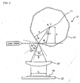
- FIG. 2 illustrates a schematic configuration of the laser processing apparatus employing the polygon mirror in accordance with the present invention.
- the polygon mirror 10 constructed with n - numbered reflection planes rotates in a constant speed at the axis 11 in an angular velocity of ⁇ and a cycle period T .
- a laser beam incident thereon is reflected from the reflection plane 12 and irradiated on the wafer 40 through the lens 20.
- the scanning angle ⁇ is twice the central angle 2 ⁇ ⁇ n on the reflection plane 12 of the polygon mirror 10. Therefore, the scanning length S L , that is a range of irradiation on the wafer 40 by the reflected laser beam applied from the reflection plane 12 of the polygon mirror 10, is determined by a morphological characteristic of the lens 20, as follows.
- S L Scanning length f : Focal distance ⁇ : Scanning angle
- a laser beam reflected from each of the reflection planes 12 of the polygon mirror 10 while the polygon mirror 10 is rotating is irradiated on the wafer 40 by the length of S L .
- the scanning length S L of a laser beam irradiated on the wafer 40 in accordance with the rotation of the polygon mirror 10 is obtained from a product of the focal length f and the scanning angle ⁇ of the laser beam reflected from the reflection plane 12 of the polygon mirror 12.
- an n-times scanning with the scanning length S L is available in every one cycle of rotation of the polygon mirror 10. That is, a laser beam irradiated on the wafer 40 is applied to the wafer 40 by the scanning length S L , overlapping in the wafer 40 by the number of the reflection planes 12 of the polygon mirror 10 when the polygon mirror 10 rotates one time.
- the scanning length S L is controllable in desired times of overlapping by varying the cycle period T or the angular velocity ⁇ of the polygon mirror 10.
- a relative wafer 40 scanning speed of the laser beam reflected from the polygon mirror 10 is enhanced by transferring the stage 30, on which the wafer 40 is settled, toward the direction reverse to the rotating direction of the polygon mirror 10.
- a wafer 40 scanning speed of the laser beam S L gets faster compared to the wafer 40 scanning speed of the laser beam when the stage 30 is standing without moving.
- Such overlaps with the scanning length S L progress along the direction reverse to the transfer direction of the stage 30 where the wafer 40 is settled.
- the wafer 40 on the stage 30 is scanned and cut out by the laser beam along the direction reverse to the transfer direction of the stage 30.
- the scanning lengths S L continuously overlap from each other in a uniform range, in which the number of overlapping times may be adjustable by controlling the transfer speed of the stage 30.
- an overlapping degree N of the scanning length may be represented in S L / l .
- the migration distance l denotes a dimension by which the stage 30 with velocity ⁇ moves for a time until one of the reflection planes 12 completes to rotate, being summarized in the following Equation 4.
- the overlapping degree N is represented in Equation 5.
- Equation 6 Nv 2 ⁇ f
- the angular velocity is obtained by dividing a product of the overlapping degree N of the laser beam and the cutout velocity ⁇ with a double value of the focal length f of the lens 20, where the cutout velocity ⁇ corresponds to the transfer speed of the stage 30 settling the wafer 40 thereon.
- FIG. 4 illustrates an exemplary embodiment of the laser processing apparatus with the polygon mirror.
- the laser processing apparatus with the polygon mirror is comprised of a controller 110 for conducting an overall operation, an input unit 120 for entering control parameters and control commands, a polygon mirror driver 130 for actuating the polygon mirror 10, a laser generator 140 for emitting laser beams, a stage transfer unit 150 for transferring the stage 30, on which the wafer 40 is settled, in a predetermined direction, a display unit 160 for informing the external users of current operating states, and a storage unit 170 for storing data relevant thereto.
- a controller 110 for conducting an overall operation
- an input unit 120 for entering control parameters and control commands
- a polygon mirror driver 130 for actuating the polygon mirror 10
- a laser generator 140 for emitting laser beams
- a stage transfer unit 150 for transferring the stage 30, on which the wafer 40 is settled, in a predetermined direction
- a display unit 160 for informing the external users of current operating states
- a storage unit 170 for storing data relevant thereto.
- the polygon mirror driver 130 includes a plurality of the reflection plane 12, being configured to make the polygon mirror 10, which has multiple planes, rotate in a predetermined velocity at the axis 11.
- the polygon mirror 10 uniformly rotates at the axis 11 in the predetermined velocity by means of a motor (not shown) under control of the controller 110.
- the laser generator 140 is configured to emit the laser beams to process the wafer 40 as an object settled on the stage 30, generating ultraviolet-ray laser beams under control of the controller 110 in this embodiment.
- the stage transfer unit 150 is configured to transfer the stage 30, on which the wafer 40 as an object to be treated is settled, in a predetermined velocity.
- laser beams emitted from the laser generator 140 are incident on the polygon mirror 10 under control of the controller 110.
- the laser beams applied to the polygon mirror 10 are reflected toward the lens 20 from the reflection planes 12, which are rotating by the polygon mirror driver 130, within the range of the scanning angle ⁇ .
- the laser beams reflected from the reflection planes 12 are condensed on the lens 20, and the condensed laser beam is irradiated on the wafer 40 in perpendicular.
- the laser beam being irradiated on the wafer 40 while one of the reflection planes 12 of the polygon mirror 10 is rotating migrates by the scanning length S L along the direction reverse to the transfer direction of the stage 30.
- FIG. 5 illustrates another embodiment of the laser processing apparatus with the polygon mirror in accordance with the present invention.
- the laser processing apparatus with the polygon mirror in accordance with another embodiment of the present invention, is basically comprised of a controller 110 for conducting an overall operation, an input unit 120 for entering control parameters and control commands, a polygon mirror driver 130 for actuating the polygon mirror 10, a laser generator 140 for emitting laser beams, a stage transfer unit 150 for transferring the stage 30, on which the wafer 40 is settled, in a predetermined direction, a display unit 160 for informing the external users of current operating states, and a storage unit 170 for storing data relevant thereto.
- a controller 110 for conducting an overall operation
- an input unit 120 for entering control parameters and control commands
- a polygon mirror driver 130 for actuating the polygon mirror 10
- a laser generator 140 for emitting laser beams
- a stage transfer unit 150 for transferring the stage 30, on which the wafer 40 is settled, in a predetermined direction
- a display unit 160 for informing the external users of current operating states
- a storage unit 170 for storing data relevant thereto.
- the laser processing apparatus with the polygon mirror in FIG. 5 is further comprised of a beam expander 210 for enlarging diameters of pointing laser beams emitted from the laser generator 140 and then applying the enlarged laser beams to the polygon mirror 10, and a beam transformer 220 for converting the laser beam, which is condensed on the lens 20 after being reflected from the polygon mirror 10, into an elliptical pattern.
- the beam transformer 220 may be easily implemented by employing a cylindrical lens.
- the enlarged laser beams incident on the polygon mirror 10 are reflected toward the lens 20 on the reflection planes 12 of the polygon mirror 10 within the range of the scanning angle ⁇ .
- the laser beam reflected from the reflection planes 12 is condensed on the lens 20, converted into an elliptical pattern by the beam transformer 220 in sectional view, and then irradiated on the wafer 40 in perpendicular.
- a long diameter of the elliptical section corresponds to a direction of cutout processing while a short diameter of the elliptical section corresponds to a width of cutout processing.
- the laser beam irradiated on the wafer 40 is shifted as the scanning length S L along the direction reverse to the transfer direction of the stage 30.
- FIG. 6 is a flow chart explaining a procedure of processing an object, in accordance with the present invention.
- first control parameters for a rotation velocity of the polygon mirror 10 and a transfer velocity of the stage 30 in the input unit 120 are established, in accordance with a type of the wafer 40 to be processed (step S10).
- Such setting operations may be simply carried out by retrieving information menus from the storage unit 170 after registering the information, that has been preliminarily designed for wafer types and processing options (e.g., cutting, grooving, and so on), in the storage unit 170.
- the controller 110 After completing the establishment for the control parameters, the controller 110 enables the polygon mirror driver 130 to rotate the polygon mirror 10 in a rotation velocity that has been predetermined at the step S10 (step S20), and also enables the stage transfer unit 150 to transfer the stage 30 in a predetermined velocity (step S30). At this point the controller 110 makes the laser generator 140 emit the laser beam (step S40).
- the laser beam emitted from the laser generator 140 is incident on the polygon mirror 10 with being enlarged in its sectional diameter after passing through the beam expander 210.
- the laser beam incident on the polygon mirror 10 is reflected from the reflection plane 12 of the polygon mirror 10 rotating at the axis 11, toward the lens 20 within the range of the scanning angle ⁇ .
- the lens 20 condenses the laser beam reflected from the polygon mirror 10, and the condensed laser beam on the lens 20 is irradiated on the wafer 40 in perpendicular after being converted into an elliptical pattern in sectional view by the beam transformer 220.
- the laser beam finally applied to the wafer 40 has a elliptical sectional pattern in which the long diameter accords to the cutout direction of the wafer 40, i.e., a progressing direction of processing, which extends an irradiation range of the laser beam over the wafer 40 a time, while the short diameter corresponds to a cutout thickness, i.e., a cutout width of processing.
- a plurality of the laser beam irradiated on the wafer 40 are overlapped in predetermined times by a plurality of the scanning length S L over the wafer 40.
- step S50 a relative speed of irradiation with the scanning length by the laser beam on the wafer 40 becomes faster which makes the wafer cutout process efficient (step S50).
- the laser beam emitted from the laser generator 140 is directly irradiated on the wafer 40 when it skips the steps of the beam expander 210 and the beam transformer 220.
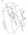
- FIG. 7 illustrates a configuration of processing the wafer 40 by the laser processing apparatus with the polygon mirror in accordance with the present invention.
- the laser beam enlarged with its sectional diameter after passing through the beam expander 210 is incident on the polygon mirror 10.
- the laser beam incident on the polygon mirror 10 is reflected within the range of the scanning angle ⁇ toward the lens 20 on the reflection plane 12 of the polygon mirror 10 that is rotating.
- the lens 20 condenses the laser beam.
- the laser beam condensed on the lens 20 is shaped into a sectional elliptical pattern by the beam transformer 220 and then irradiated on the wafer 40.
- the long diameter of the ellipse is associated with a progressing direction on the wafer 40 by the laser beam while the short diameter of the ellipse is associated with a cutout width on the wafer 40 by the laser beam.
- the elliptical laser beam irradiated on the wafer 40 is progressing along the direction of its long diameter, accompanying with the cutout width by its short diameter.
- the cutout width 41 of the wafer 40 is adjustable by controlling the short diameter of the elliptical section of the laser beam, which is established by the beam transformer 220.
- a cutout section 42 has a slope throughout the cutout process, by which vapors escaping from the wafer material due to the irradiation of the laser beam are easily discharged without depositing on the cutout plane 42 during the process.
- the wafer processing is carried out easily without such as a recasting effect for which vapors from the wafer material are deposited on the cutout wall 43 of the wafer 40.
- the present invention is also available to processing other substrates or boards such as plastics, metals, and so on.
- the laser processing apparatus with the polygon mirror in accordance with the present invention needs not any change of additional devices because a laser beam is enough to perform the cutout process, which enables the process to be rapidly carried out in easy and efficiency. Furthermore, since the present invention provides an efficient technique to able to control the cutout width by adjusting the short diameter of the elliptical laser beam and to prevent a recasting effect that causes vapors escaping from an object to be cut out, it is advantageous to processing a wafer in highly precise operations, as well as normal objects.
Landscapes
- Physics & Mathematics (AREA)
- Optics & Photonics (AREA)
- Engineering & Computer Science (AREA)
- Plasma & Fusion (AREA)
- Mechanical Engineering (AREA)
- Multimedia (AREA)
- General Physics & Mathematics (AREA)
- Laser Beam Processing (AREA)
- Mechanical Optical Scanning Systems (AREA)
- Recrystallisation Techniques (AREA)
Claims (11)
- Laserbearbeitungsvorrichtung mit einem Polygonspiegel (10) zum Bearbeiten eines Objektes (40) mit einem Laserstrahl, mit:einem Lasergenerator (140) zum Emittieren des Laserstrahls,einem Polygonspiegel (10), der aus einer Mehrzahl von Reflektionsflächen (12) aufgebaut ist, die den Laserstrahl reflektieren, der von dem Lasergenerator (140) emittiert wird, während diese um eine Achse (11) rotieren,einer Linse (20) zum Bündeln des von dem Polygonspiegel (10) reflektierten Laserstrahls und zum Einstrahlen des Laserstrahls auf das Objekt (40),einer Bühne (30) zum Absetzen des Objektes,gekennzeichnet durch
eine Bühnentransfereinheit (150) zum Transferieren der Bühne in einer vorbestimmten Richtung,
einen Controller (110) zum Steuern der Bühnentransfereinheit (150), und
einen Polygonspiegeltreiber (130) zum Rotieren des Polygonspiegels (10) mit einer konstanten Geschwindigkeit, um die Reflektionsflächen (12) mit einer vorbestimmten Winkelgeschwindigkeit umlaufen zu lassen,
wobei der Controller (110) derart aufgebaut ist, um den Polygonspiegeltreiber (130) und die Bühnentransfereinheit (150) zu steuern, um die Bühne (30) entgegen einer Rotationsrichtung des Polygonspiegels (110) und entgegen der Ablaufrichtung des Laserstrahl zu transferieren. - Laserbearbeitungsvorrichtung mit dem Polygonspiegel (10) nach Anspruch 1, ferner umfassend einen Strahlwandler (220) zum Umwandeln eines Abschnittsmusters des Laserstrahls, der an der Linse (20) gebündelt ist, in eine Ellipse.
- Laserbearbeitungsvorrichtung mit dem Polygonspiegel (10) nach Anspruch 2, wobei der Controller (110) den Strahlumwandler (220) steuert, um den Laserstrahl so umzuwandeln, dass dieser mit dem Abschnittsmuster als der Ellipse so geformt ist, dass deren Hauptachse entlang einer Fortschrittsrichtung ausgerichtet ist, und dann den umgewandelten Laserstrahl auf das Objekt (40) einstrahlt.
- Laserbearbeitungsvorrichtung mit dem Polygonspiegel (10) nach Anspruch 5, wobei der Controller (110) eine Nebenachse des elliptischen Abschnitts des umgewandelten Laserstrahls zum Justieren der Verarbeitungsbreite durch den Laserstrahl steuert.
- Laserbearbeitungsvorrichtung mit dem Polygonspiegel (10) nach einem der vorstehenden Ansprüche, wobei das Objekt (40), das durch den Laserstrahl bearbeitet wird, ein Wafer ist.
- Laserbearbeitungsvorrichtung mit dem Polygonspiegel (10) nach einem der vorstehenden Ansprüche, ferner mit einem Strahlausdehner (210) zum Vergrößern eines Abschnittsdurchmessers des Laserstrahls, der von dem Lasergenerator (140) emittiert wird, wobei der vergrößerte Laserstrahl an der Linse (20) gebündelt wird, nachdem er an dem Polygonspiegel (10) reflektiert wurde, und auf den Strahlumformer (220) gerichtet wird.
- Laserbearbeitungsvorrichtung mit dem Polygonspiegel (10) nach Anspruch 5, wobei die Linse (20) den Laserstrahl daran bündelt und dann den Laserstrahl senkrecht auf den Wafer (40) einstrahlt.
- Laserbearbeitungsvorrichtung mit dem Polygonspiegel (10) nach Anspruch 5, wobei der Controller (110) eine Abtastlänge des Laserstrahls, der auf den Wafer (40) gerichtet ist, durch eine der Reflektionsflächen (12) entsprechend mit der Rotation des Polygonspiegels (10) durch das Produkt einer Brennweite der Linse (20) und einem Abtastwinkel des Laserstrahls, der von den Reflektionsflächen (12) des Polygonspiegels (10) reflektiert ist, steuert.
- Laserbearbeitungsvorrichtung mit dem Polygonspiegel (10) nach Anspruch 8, wobei der Controller (110) den Abtastwinkel des Laserstrahls steuert, um ein Reflektionswinkel zu sein, der durch die Anfangs- und Endteile der Reflektionsfläche (12) gebildet ist.
- Laserbearbeitungsvorrichtung mit dem Polygonspiegel (10) nach Anspruch 5, wobei der Laserstrahl, der von der Reflektionsfläche (12) reflektiert wird, entsprechend der Rotation des Polygonspiegels (10) auf den Wafer (40) eingestrahlt wird, wobei er in einer vorbestimmten Anzahl überlappt wird, und wobei der Controller (110) die vorbestimmte Anzahl von Überlappungen durch Justieren einer Winkelgeschwindigkeit des Polygonspiegels (10) während eines Konstant-Haltens einer Transfergeschwindigkeit der Bühne (30) steuert.
- Laserbearbeitungsvorrichtung mit dem Polygonspiegel (10) nach Anspruch 5, wobei der Laserstrahl, der von der Reflektionsfläche (12) reflektiert wird, entsprechend der Rotation des Polygonspiegels (10) auf den Wafer (40) eingestrahlt wird, wobei er in einer vorbestimmten Anzahl überlappt wird, und wobei der Controller (110) die vorbestimmte Anzahl von Überlappungen durch Justieren einer Transfergeschwindigkeit der Bühne (30) während eines Konstant-Haltens einer Winkelgeschwindigkeit des Polygonspiegels (10) steuert.
Applications Claiming Priority (2)
| Application Number | Priority Date | Filing Date | Title |
|---|---|---|---|
| KR2004022270 | 2004-03-31 | ||
| KR1020040022270A KR100462358B1 (ko) | 2004-03-31 | 2004-03-31 | 폴리곤 미러를 이용한 레이저 가공장치 |
Publications (2)
| Publication Number | Publication Date |
|---|---|
| EP1586406A1 EP1586406A1 (de) | 2005-10-19 |
| EP1586406B1 true EP1586406B1 (de) | 2007-10-31 |
Family
ID=34925414
Family Applications (1)
| Application Number | Title | Priority Date | Filing Date |
|---|---|---|---|
| EP04014434A Expired - Lifetime EP1586406B1 (de) | 2004-03-31 | 2004-06-19 | Laserbearbeitungsvorrichtung mit einem Polygonspiegel |
Country Status (11)
| Country | Link |
|---|---|
| US (1) | US20050218128A1 (de) |
| EP (1) | EP1586406B1 (de) |
| JP (1) | JP4044539B2 (de) |
| KR (1) | KR100462358B1 (de) |
| CN (1) | CN100363143C (de) |
| AT (1) | ATE376902T1 (de) |
| CA (1) | CA2472411A1 (de) |
| DE (1) | DE602004009754T2 (de) |
| MY (1) | MY137166A (de) |
| SG (1) | SG130943A1 (de) |
| TW (1) | TWI241060B (de) |
Families Citing this family (33)
| Publication number | Priority date | Publication date | Assignee | Title |
|---|---|---|---|---|
| KR100462359B1 (ko) | 2004-08-18 | 2004-12-17 | 주식회사 이오테크닉스 | 폴리곤 미러를 이용한 레이저 가공장치 및 방법 |
| KR20080028559A (ko) * | 2006-09-27 | 2008-04-01 | 주식회사 이오테크닉스 | 폴리곤 미러를 이용한 대상물 다중 가공 방법 |
| EP1990168B1 (de) * | 2007-05-10 | 2012-06-27 | Grenzebach Maschinenbau GmbH | Verfahren zum laserthermischen Trennen von keramischem oder anderem spröden Plattenmaterial |
| ATE482050T1 (de) | 2007-06-30 | 2010-10-15 | Trumpf Werkzeugmaschinen Gmbh | Maschine zum bearbeiten von werkstücken und verfahren zum maschinellen bearbeiten von werkstücken |
| DE502007002935D1 (de) * | 2007-06-30 | 2010-04-08 | Trumpf Werkzeugmaschinen Gmbh | Werkzeugmaschine und Verfahren zum Bearbeiten eines Werkstückes |
| KR100884629B1 (ko) * | 2007-08-06 | 2009-02-23 | 주식회사 이오테크닉스 | 레이저 가공 장치 및 방법 |
| CN102046345A (zh) * | 2008-04-15 | 2011-05-04 | 三星钻石工业股份有限公司 | 脆性材料基板的加工方法 |
| CN101829846A (zh) * | 2010-05-11 | 2010-09-15 | 苏州市博海激光科技有限公司 | 高功率激光辊类表面集成聚焦毛化加工方法及装置 |
| CN101913026A (zh) * | 2010-06-30 | 2010-12-15 | 苏州市博海激光科技有限公司 | 卷烟接装纸双头集成激光打孔装置 |
| DE102011108405A1 (de) * | 2011-07-23 | 2013-01-24 | Volkswagen Aktiengesellschaft | Verfahren und Vorrichtung zum Einbringen einer Schnittfuge in ein Werkstück |
| KR101312937B1 (ko) | 2011-10-19 | 2013-10-01 | 한국기계연구원 | 웨이퍼 다이싱용 레이저 개질 장치 및 웨이퍼 다이싱 방법 |
| JP5861494B2 (ja) * | 2012-02-23 | 2016-02-16 | 三菱マテリアル株式会社 | レーザ加工装置およびレーザ加工方法 |
| CN104981318B (zh) * | 2013-02-13 | 2017-03-08 | 住友化学株式会社 | 激光照射装置及光学构件贴合体的制造装置 |
| CN103433619B (zh) * | 2013-08-30 | 2015-10-21 | 大族激光科技产业集团股份有限公司 | 激光熔覆打印机及线路板的制作方法 |
| JP6189178B2 (ja) * | 2013-10-29 | 2017-08-30 | 株式会社ディスコ | レーザー加工装置 |
| JP6434360B2 (ja) * | 2015-04-27 | 2018-12-05 | 株式会社ディスコ | レーザー加工装置 |
| WO2016189344A1 (en) | 2015-05-28 | 2016-12-01 | University Of West Bohemia | Method of laser beam writing with shifted laser surface texturing |
| US10942257B2 (en) | 2016-12-31 | 2021-03-09 | Innovusion Ireland Limited | 2D scanning high precision LiDAR using combination of rotating concave mirror and beam steering devices |
| JP6997566B2 (ja) | 2017-09-14 | 2022-01-17 | 株式会社ディスコ | レーザー加工装置 |
| US11493601B2 (en) | 2017-12-22 | 2022-11-08 | Innovusion, Inc. | High density LIDAR scanning |
| WO2020013890A2 (en) | 2018-02-23 | 2020-01-16 | Innovusion Ireland Limited | Multi-wavelength pulse steering in lidar systems |
| WO2019165294A1 (en) | 2018-02-23 | 2019-08-29 | Innovusion Ireland Limited | 2-dimensional steering system for lidar systems |
| JP6592563B1 (ja) | 2018-07-06 | 2019-10-16 | 株式会社アマダホールディングス | レーザ加工機及びレーザ加工方法 |
| JP6592564B1 (ja) | 2018-07-06 | 2019-10-16 | 株式会社アマダホールディングス | レーザ加工機及びレーザ加工方法 |
| DE102018212281A1 (de) * | 2018-07-24 | 2020-01-30 | Amada Holdings Co., Ltd. | Laserverarbeitungsmaschine und Laserverarbeitungsverfahren |
| JP7011557B2 (ja) * | 2018-09-07 | 2022-01-26 | 川崎重工業株式会社 | レーザ光走査装置及びレーザ加工装置 |
| CN109465252B (zh) * | 2019-01-11 | 2023-09-26 | 桂林电子科技大学 | 超声辅助激光水下清洗装置及方法 |
| CN117850023A (zh) * | 2019-04-01 | 2024-04-09 | 川崎重工业株式会社 | 光反射装置、导光装置以及光扫描装置 |
| CN110153106B (zh) * | 2019-04-29 | 2024-02-13 | 苏州创鑫激光科技有限公司 | 一种激光清洗系统以及清洗方法 |
| US10903121B1 (en) * | 2019-08-14 | 2021-01-26 | Applied Materials, Inc. | Hybrid wafer dicing approach using a uniform rotating beam laser scribing process and plasma etch process |
| CN112880976B (zh) * | 2021-01-14 | 2023-02-28 | 歌尔股份有限公司 | 入射光束的角度调节装置和反射器件的制造方法 |
| CN116921872B (zh) * | 2023-06-27 | 2025-11-11 | 广东原点智能技术有限公司 | 一种激光平面磨削方法 |
| TWI872705B (zh) * | 2023-09-15 | 2025-02-11 | 財團法人工業技術研究院 | 連續式雷射加工系統及加工方法 |
Family Cites Families (17)
| Publication number | Priority date | Publication date | Assignee | Title |
|---|---|---|---|---|
| JPS6048732B2 (ja) * | 1977-02-04 | 1985-10-29 | キヤノン株式会社 | 自己増幅偏向走査光学系 |
| US5072244A (en) * | 1987-11-30 | 1991-12-10 | Canon Kabushiki Kaisha | Superposed image forming apparatus with plural and adjustable image forming stations |
| JPH01306088A (ja) * | 1988-06-01 | 1989-12-11 | Nippei Toyama Corp | 可変ビームレーザ加工装置 |
| EP0483569A1 (de) * | 1990-10-29 | 1992-05-06 | Fmc Corporation | Vorrichtung zum Verschweissen von Kunststoffen |
| JPH0639572A (ja) * | 1991-01-11 | 1994-02-15 | Souei Tsusho Kk | ウェハ割断装置 |
| WO2004085108A1 (ja) * | 1993-08-05 | 2004-10-07 | Nobuhiko Tada | リードフレーム加工方法及びリードフレーム加工装置 |
| KR960705652A (ko) * | 1993-11-19 | 1996-11-08 | 안자키 사토루 | 레이저마아킹장치 및 방법(laser marking method and apparatus therefor) |
| JP3192552B2 (ja) * | 1994-05-23 | 2001-07-30 | 松下電器産業株式会社 | 走査光学系およびそれを用いた画像形成装置 |
| US5943153A (en) * | 1995-04-21 | 1999-08-24 | Minolta Co., Ltd. | Lens holding apparatus and a light-beam scanning optical apparatus |
| JP3373367B2 (ja) * | 1996-08-09 | 2003-02-04 | 松下電器産業株式会社 | 3次元計測装置及び3次元計測方法 |
| US6061080A (en) * | 1998-01-30 | 2000-05-09 | Xerox Corporation | Aperture for multiple reflection raster output scanning system to reduce bow |
| JP3178524B2 (ja) * | 1998-11-26 | 2001-06-18 | 住友重機械工業株式会社 | レーザマーキング方法と装置及びマーキングされた部材 |
| US6300590B1 (en) * | 1998-12-16 | 2001-10-09 | General Scanning, Inc. | Laser processing |
| US6538230B2 (en) * | 2001-05-17 | 2003-03-25 | Preco Laser Systems, Llc | Method and apparatus for improving laser hole resolution |
| WO2003036391A1 (en) * | 2001-10-25 | 2003-05-01 | Toray Engineering Company,Limited | Method and device for marking identification code by laser beam |
| JP2003177553A (ja) * | 2001-12-13 | 2003-06-27 | Dainippon Screen Mfg Co Ltd | レーザ描画方法とその装置 |
| US6788445B2 (en) * | 2002-01-14 | 2004-09-07 | Applied Materials, Inc. | Multi-beam polygon scanning system |
-
2004
- 2004-03-31 KR KR1020040022270A patent/KR100462358B1/ko not_active Expired - Fee Related
- 2004-06-17 TW TW093117466A patent/TWI241060B/zh not_active IP Right Cessation
- 2004-06-19 AT AT04014434T patent/ATE376902T1/de not_active IP Right Cessation
- 2004-06-19 EP EP04014434A patent/EP1586406B1/de not_active Expired - Lifetime
- 2004-06-19 DE DE602004009754T patent/DE602004009754T2/de not_active Expired - Lifetime
- 2004-06-23 CA CA002472411A patent/CA2472411A1/en not_active Abandoned
- 2004-06-24 JP JP2004185947A patent/JP4044539B2/ja not_active Expired - Fee Related
- 2004-06-25 MY MYPI20042518A patent/MY137166A/en unknown
- 2004-07-06 US US10/886,122 patent/US20050218128A1/en not_active Abandoned
- 2004-07-06 SG SG200406612-2A patent/SG130943A1/en unknown
- 2004-07-29 CN CNB2004100590467A patent/CN100363143C/zh not_active Expired - Fee Related
Also Published As
| Publication number | Publication date |
|---|---|
| TWI241060B (en) | 2005-10-01 |
| DE602004009754T2 (de) | 2008-08-28 |
| CN100363143C (zh) | 2008-01-23 |
| TW200533022A (en) | 2005-10-01 |
| CN1676269A (zh) | 2005-10-05 |
| US20050218128A1 (en) | 2005-10-06 |
| KR100462358B1 (ko) | 2004-12-17 |
| JP4044539B2 (ja) | 2008-02-06 |
| ATE376902T1 (de) | 2007-11-15 |
| CA2472411A1 (en) | 2005-09-30 |
| SG130943A1 (en) | 2007-04-26 |
| DE602004009754D1 (de) | 2007-12-13 |
| EP1586406A1 (de) | 2005-10-19 |
| JP2005288541A (ja) | 2005-10-20 |
| MY137166A (en) | 2009-01-30 |
Similar Documents
| Publication | Publication Date | Title |
|---|---|---|
| EP1586406A1 (de) | Laserbearbeitungsvorrichtung mit einem Polygonspiegel | |
| JP4027930B2 (ja) | ポリゴンミラーと利用したレーザー加工装置及び方法 | |
| US6720524B1 (en) | Method and apparatus for laser drilling | |
| EP1738409B1 (de) | Laser-verarbeitungsvorrichtungen und -verfahren | |
| CN1301178C (zh) | 半导体中微结构的紫外线激光烧蚀的图案化 | |
| JP2004268144A (ja) | レーザ加工装置 | |
| JP7746429B2 (ja) | レーザ加工装置、及び、レーザ加工方法 | |
| US5282921A (en) | Apparatus and method for optimally scanning a two-dimensional surface of one or more objects | |
| KR102309247B1 (ko) | 레이저빔 조사 장치 및 이를 포함하는 기판 처리 시스템, 기판 처리 방법 | |
| KR100603904B1 (ko) | 폴리곤 미러를 이용한 다중 레이저 가공장치 | |
| KR20060012396A (ko) | 다중 레이저 가공장치 | |
| JPWO2021100421A1 (ja) | ワーク分離装置及びワーク分離方法 | |
| JP2021093487A (ja) | レーザアニール装置および半導体装置の製造方法 | |
| US6265138B1 (en) | Process and apparatus for oblique beam revolution, for the effective laser stripping of sidewalls | |
| JP7339031B2 (ja) | レーザー加工装置 | |
| JP2004098120A (ja) | レーザ加工方法及びレーザ加工装置 | |
| KR100664573B1 (ko) | 레이저 가공 장치 및 방법 | |
| CN120604323A (zh) | 倒角加工方法及倒角加工装置 | |
| WO2025142689A1 (ja) | 対象物加工方法及び半導体デバイスの製造方法 | |
| JPH10263872A (ja) | レーザ加工機 | |
| JP2026022663A (ja) | 被加工物の加工方法、被加工物の面取り加工方法、および、基板の製造方法 | |
| JP2017177214A (ja) | 基板加工方法および基板加工装置 | |
| CN120816176A (zh) | 一种高效率的晶圆激光剥片方法及系统 |
Legal Events
| Date | Code | Title | Description |
|---|---|---|---|
| PUAI | Public reference made under article 153(3) epc to a published international application that has entered the european phase |
Free format text: ORIGINAL CODE: 0009012 |
|
| 17P | Request for examination filed |
Effective date: 20050621 |
|
| AK | Designated contracting states |
Kind code of ref document: A1 Designated state(s): AT BE BG CH CY CZ DE DK EE ES FI FR GB GR HU IE IT LI LU MC NL PL PT RO SE SI SK TR |
|
| AX | Request for extension of the european patent |
Extension state: AL HR LT LV MK |
|
| AKX | Designation fees paid |
Designated state(s): AT BE BG CH CY CZ DE DK EE ES FI FR GB GR HU IE IT LI LU MC NL PL PT RO SE SI SK TR |
|
| GRAP | Despatch of communication of intention to grant a patent |
Free format text: ORIGINAL CODE: EPIDOSNIGR1 |
|
| GRAS | Grant fee paid |
Free format text: ORIGINAL CODE: EPIDOSNIGR3 |
|
| GRAA | (expected) grant |
Free format text: ORIGINAL CODE: 0009210 |
|
| AK | Designated contracting states |
Kind code of ref document: B1 Designated state(s): AT BE BG CH CY CZ DE DK EE ES FI FR GB GR HU IE IT LI LU MC NL PL PT RO SE SI SK TR |
|
| REG | Reference to a national code |
Ref country code: GB Ref legal event code: FG4D |
|
| REG | Reference to a national code |
Ref country code: IE Ref legal event code: FG4D |
|
| REG | Reference to a national code |
Ref country code: CH Ref legal event code: EP |
|
| REF | Corresponds to: |
Ref document number: 602004009754 Country of ref document: DE Date of ref document: 20071213 Kind code of ref document: P |
|
| NLV1 | Nl: lapsed or annulled due to failure to fulfill the requirements of art. 29p and 29m of the patents act | ||
| PG25 | Lapsed in a contracting state [announced via postgrant information from national office to epo] |
Ref country code: SE Free format text: LAPSE BECAUSE OF FAILURE TO SUBMIT A TRANSLATION OF THE DESCRIPTION OR TO PAY THE FEE WITHIN THE PRESCRIBED TIME-LIMIT Effective date: 20080131 Ref country code: LI Free format text: LAPSE BECAUSE OF FAILURE TO SUBMIT A TRANSLATION OF THE DESCRIPTION OR TO PAY THE FEE WITHIN THE PRESCRIBED TIME-LIMIT Effective date: 20071031 Ref country code: NL Free format text: LAPSE BECAUSE OF FAILURE TO SUBMIT A TRANSLATION OF THE DESCRIPTION OR TO PAY THE FEE WITHIN THE PRESCRIBED TIME-LIMIT Effective date: 20071031 Ref country code: CH Free format text: LAPSE BECAUSE OF FAILURE TO SUBMIT A TRANSLATION OF THE DESCRIPTION OR TO PAY THE FEE WITHIN THE PRESCRIBED TIME-LIMIT Effective date: 20071031 Ref country code: ES Free format text: LAPSE BECAUSE OF FAILURE TO SUBMIT A TRANSLATION OF THE DESCRIPTION OR TO PAY THE FEE WITHIN THE PRESCRIBED TIME-LIMIT Effective date: 20080211 |
|
| REG | Reference to a national code |
Ref country code: CH Ref legal event code: PL |
|
| PG25 | Lapsed in a contracting state [announced via postgrant information from national office to epo] |
Ref country code: PL Free format text: LAPSE BECAUSE OF FAILURE TO SUBMIT A TRANSLATION OF THE DESCRIPTION OR TO PAY THE FEE WITHIN THE PRESCRIBED TIME-LIMIT Effective date: 20071031 Ref country code: BG Free format text: LAPSE BECAUSE OF FAILURE TO SUBMIT A TRANSLATION OF THE DESCRIPTION OR TO PAY THE FEE WITHIN THE PRESCRIBED TIME-LIMIT Effective date: 20080131 Ref country code: SI Free format text: LAPSE BECAUSE OF FAILURE TO SUBMIT A TRANSLATION OF THE DESCRIPTION OR TO PAY THE FEE WITHIN THE PRESCRIBED TIME-LIMIT Effective date: 20071031 Ref country code: PT Free format text: LAPSE BECAUSE OF FAILURE TO SUBMIT A TRANSLATION OF THE DESCRIPTION OR TO PAY THE FEE WITHIN THE PRESCRIBED TIME-LIMIT Effective date: 20080331 |
|
| ET | Fr: translation filed | ||
| PG25 | Lapsed in a contracting state [announced via postgrant information from national office to epo] |
Ref country code: AT Free format text: LAPSE BECAUSE OF FAILURE TO SUBMIT A TRANSLATION OF THE DESCRIPTION OR TO PAY THE FEE WITHIN THE PRESCRIBED TIME-LIMIT Effective date: 20071031 |
|
| PG25 | Lapsed in a contracting state [announced via postgrant information from national office to epo] |
Ref country code: DK Free format text: LAPSE BECAUSE OF FAILURE TO SUBMIT A TRANSLATION OF THE DESCRIPTION OR TO PAY THE FEE WITHIN THE PRESCRIBED TIME-LIMIT Effective date: 20071031 Ref country code: CZ Free format text: LAPSE BECAUSE OF FAILURE TO SUBMIT A TRANSLATION OF THE DESCRIPTION OR TO PAY THE FEE WITHIN THE PRESCRIBED TIME-LIMIT Effective date: 20071031 |
|
| PG25 | Lapsed in a contracting state [announced via postgrant information from national office to epo] |
Ref country code: SK Free format text: LAPSE BECAUSE OF FAILURE TO SUBMIT A TRANSLATION OF THE DESCRIPTION OR TO PAY THE FEE WITHIN THE PRESCRIBED TIME-LIMIT Effective date: 20071031 Ref country code: RO Free format text: LAPSE BECAUSE OF FAILURE TO SUBMIT A TRANSLATION OF THE DESCRIPTION OR TO PAY THE FEE WITHIN THE PRESCRIBED TIME-LIMIT Effective date: 20071031 Ref country code: BE Free format text: LAPSE BECAUSE OF FAILURE TO SUBMIT A TRANSLATION OF THE DESCRIPTION OR TO PAY THE FEE WITHIN THE PRESCRIBED TIME-LIMIT Effective date: 20071031 |
|
| PLBE | No opposition filed within time limit |
Free format text: ORIGINAL CODE: 0009261 |
|
| STAA | Information on the status of an ep patent application or granted ep patent |
Free format text: STATUS: NO OPPOSITION FILED WITHIN TIME LIMIT |
|
| 26N | No opposition filed |
Effective date: 20080801 |
|
| PG25 | Lapsed in a contracting state [announced via postgrant information from national office to epo] |
Ref country code: GR Free format text: LAPSE BECAUSE OF FAILURE TO SUBMIT A TRANSLATION OF THE DESCRIPTION OR TO PAY THE FEE WITHIN THE PRESCRIBED TIME-LIMIT Effective date: 20080201 Ref country code: MC Free format text: LAPSE BECAUSE OF NON-PAYMENT OF DUE FEES Effective date: 20080630 |
|
| PG25 | Lapsed in a contracting state [announced via postgrant information from national office to epo] |
Ref country code: FI Free format text: LAPSE BECAUSE OF FAILURE TO SUBMIT A TRANSLATION OF THE DESCRIPTION OR TO PAY THE FEE WITHIN THE PRESCRIBED TIME-LIMIT Effective date: 20071031 |
|
| PG25 | Lapsed in a contracting state [announced via postgrant information from national office to epo] |
Ref country code: EE Free format text: LAPSE BECAUSE OF FAILURE TO SUBMIT A TRANSLATION OF THE DESCRIPTION OR TO PAY THE FEE WITHIN THE PRESCRIBED TIME-LIMIT Effective date: 20071031 |
|
| PG25 | Lapsed in a contracting state [announced via postgrant information from national office to epo] |
Ref country code: CY Free format text: LAPSE BECAUSE OF FAILURE TO SUBMIT A TRANSLATION OF THE DESCRIPTION OR TO PAY THE FEE WITHIN THE PRESCRIBED TIME-LIMIT Effective date: 20071031 |
|
| PG25 | Lapsed in a contracting state [announced via postgrant information from national office to epo] |
Ref country code: HU Free format text: LAPSE BECAUSE OF FAILURE TO SUBMIT A TRANSLATION OF THE DESCRIPTION OR TO PAY THE FEE WITHIN THE PRESCRIBED TIME-LIMIT Effective date: 20080501 Ref country code: LU Free format text: LAPSE BECAUSE OF NON-PAYMENT OF DUE FEES Effective date: 20080619 |
|
| PG25 | Lapsed in a contracting state [announced via postgrant information from national office to epo] |
Ref country code: TR Free format text: LAPSE BECAUSE OF FAILURE TO SUBMIT A TRANSLATION OF THE DESCRIPTION OR TO PAY THE FEE WITHIN THE PRESCRIBED TIME-LIMIT Effective date: 20071031 |
|
| PG25 | Lapsed in a contracting state [announced via postgrant information from national office to epo] |
Ref country code: IT Free format text: LAPSE BECAUSE OF NON-PAYMENT OF DUE FEES Effective date: 20080630 |
|
| REG | Reference to a national code |
Ref country code: FR Ref legal event code: PLFP Year of fee payment: 13 |
|
| REG | Reference to a national code |
Ref country code: FR Ref legal event code: PLFP Year of fee payment: 14 |
|
| PGFP | Annual fee paid to national office [announced via postgrant information from national office to epo] |
Ref country code: IE Payment date: 20170622 Year of fee payment: 14 |
|
| PGFP | Annual fee paid to national office [announced via postgrant information from national office to epo] |
Ref country code: FR Payment date: 20180627 Year of fee payment: 7 |
|
| REG | Reference to a national code |
Ref country code: IE Ref legal event code: MM4A |
|
| PG25 | Lapsed in a contracting state [announced via postgrant information from national office to epo] |
Ref country code: FR Free format text: LAPSE BECAUSE OF NON-PAYMENT OF DUE FEES Effective date: 20180630 Ref country code: IE Free format text: LAPSE BECAUSE OF NON-PAYMENT OF DUE FEES Effective date: 20180619 |
|
| GBPC | Gb: european patent ceased through non-payment of renewal fee |
Effective date: 20190619 |
|
| PG25 | Lapsed in a contracting state [announced via postgrant information from national office to epo] |
Ref country code: GB Free format text: LAPSE BECAUSE OF NON-PAYMENT OF DUE FEES Effective date: 20190619 |
|
| PGFP | Annual fee paid to national office [announced via postgrant information from national office to epo] |
Ref country code: DE Payment date: 20220627 Year of fee payment: 19 |
|
| REG | Reference to a national code |
Ref country code: DE Ref legal event code: R119 Ref document number: 602004009754 Country of ref document: DE |
|
| PG25 | Lapsed in a contracting state [announced via postgrant information from national office to epo] |
Ref country code: DE Free format text: LAPSE BECAUSE OF NON-PAYMENT OF DUE FEES Effective date: 20240103 |