EP1585243B1 - Méthode et dispositif de demultiplexage de trains de signaux numériques - Google Patents
Méthode et dispositif de demultiplexage de trains de signaux numériques Download PDFInfo
- Publication number
- EP1585243B1 EP1585243B1 EP05270025A EP05270025A EP1585243B1 EP 1585243 B1 EP1585243 B1 EP 1585243B1 EP 05270025 A EP05270025 A EP 05270025A EP 05270025 A EP05270025 A EP 05270025A EP 1585243 B1 EP1585243 B1 EP 1585243B1
- Authority
- EP
- European Patent Office
- Prior art keywords
- srts
- signal
- incoming
- value
- outgoing
- Prior art date
- Legal status (The legal status is an assumption and is not a legal conclusion. Google has not performed a legal analysis and makes no representation as to the accuracy of the status listed.)
- Expired - Lifetime
Links
Images


Classifications
-
- H—ELECTRICITY
- H04—ELECTRIC COMMUNICATION TECHNIQUE
- H04L—TRANSMISSION OF DIGITAL INFORMATION, e.g. TELEGRAPHIC COMMUNICATION
- H04L5/00—Arrangements affording multiple use of the transmission path
-
- H—ELECTRICITY
- H04—ELECTRIC COMMUNICATION TECHNIQUE
- H04J—MULTIPLEX COMMUNICATION
- H04J3/00—Time-division multiplex systems
- H04J3/16—Time-division multiplex systems in which the time allocation to individual channels within a transmission cycle is variable, e.g. to accommodate varying complexity of signals, to vary number of channels transmitted
- H04J3/1605—Fixed allocated frame structures
- H04J3/1623—Plesiochronous digital hierarchy [PDH]
- H04J3/1641—Hierarchical systems
-
- H—ELECTRICITY
- H04—ELECTRIC COMMUNICATION TECHNIQUE
- H04J—MULTIPLEX COMMUNICATION
- H04J3/00—Time-division multiplex systems
- H04J3/02—Details
- H04J3/06—Synchronising arrangements
- H04J3/062—Synchronisation of signals having the same nominal but fluctuating bit rates, e.g. using buffers
- H04J3/0632—Synchronisation of packets and cells, e.g. transmission of voice via a packet network, circuit emulation service [CES]
-
- H—ELECTRICITY
- H04—ELECTRIC COMMUNICATION TECHNIQUE
- H04J—MULTIPLEX COMMUNICATION
- H04J3/00—Time-division multiplex systems
- H04J3/02—Details
- H04J3/06—Synchronising arrangements
- H04J3/07—Synchronising arrangements using pulse stuffing for systems with different or fluctuating information rates or bit rates
- H04J3/073—Bit stuffing, e.g. PDH
Definitions
- the invention resides generally in the field of multiplexing and/or demultiplexing of a plurality of digital signal streams.
- it relates to rate adjustment of digital signal streams in connection with multiplexing/demultiplexing by using SRTS (Synchronous Residual Time Stamp) values.
- SRTS Synchronous Residual Time Stamp
- digital signal streams are transported at a variety of rates, synchronously or asynchronously, and in all cases, clocks are used for processing these digital signal streams. These clocks must be brought into synchrony for proper data exchange and timing information of some form is transported from the source to destination.
- Digital signal streams are also frequently regenerated at a proper rate as they experience signal deterioration by noise, delays, jitter etc. They are also multiplexed to produce higher bit rates for higher capacity transmission systems, as a means of utilizing the same transmission medium economically for may different users.
- multiplexing there are more than one digital transmission hierarchies for telecommunications for different parts of the world.
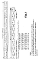
- Figure 1 shows one example of digital hierarchies used in North America.
- DS1 signal streams are multiplexed into one DS2 signal stream and 7 DS2 signal streams are then multiplexed into a DS3 signal stream.
- the bit rates of levels are also shown in the Figure.
- a major problem of multiplexing involves synchronizing the input signal streams. Digital signal streams cannot be directly interleaved and guaranteed their subsequent identification unless the pulse rates of all the signal sources are locked to a common clock. This means that all the signal streams are frequency synchronous, or else they are asynchronous and brought into frequency synchronism by the multiplexer.
- the multiplexer system can establish frequency synchronism by increasing the bit rate of each separate input to one common rate before combining them into one bit stream. This adds extra time slots into which extra pulses can be stuffed.
- pulse stuffing all incoming digital signal streams are stuffed with a sufficient number of pulses to raise each of their rates to that of the desired common rate.
- demultiplexing a single signal stream of a high rate is split into a plurality of signal streams. Each of the split signal streams is stripped of stuffed bits which are so identified and is desynchronized into a single signal stream of a lower rate according to the common clock.
- Figure 2 shows the structure of a DS2 signal stream which consists of 1176 bits in a frame called M-frame which is made up of 4 subframes, each of 294 bits.
- the DS1 data rate can be adjusted by changing how often the stuff position is used for null bit or data bit.
- FIG. 3 shows the structure of DS3 signal stream.
- a DS3 stream consists 4,760 in an M-frame which is made up of 7 subframes, each of 680 bits.
- the stuff position in each subframe is also arranged in a similar fashion as in DS2 stream. Therefore in a DS3 stream, there are 7 stuff positions in one M-frame, one per DS2.
- a broadband network such as SONET handles ATM traffic in addition to other synchronous traffic. While a network is synchronous in operation, ATM traffic is asynchronous in nature and thus such a data stream experiences the cell jitter, cell delay variation and other fluctuations as it moves through the network toward a destination node. Even when an ATM network is transporting a CBR (constant bit rate) stream between a source node and a destination node, the clock frequency at the destination node cannot be traced directly back to that of the source node by the regular, periodic arrival of the CBR stream. A few techniques have been used to convey the difference between the network clock frequency and the service clock frequency (frequency of the data being transported). U.S. Patent No. 5,260,978 Nov.
- SRTS Synchronous Residual Time Stamp
- P bits small overhead bits
- the resolution is governed by the nominal value of the frequency difference and the clock tolerance, and determines the required minimum number of P-bits. Under normally expected parameters, these P-bits would be significantly smaller than the number of bits that would be required to express the clock frequencies, e.g. 3 bits instead of 13 bits.
- a typical sampling period is 3008 which corresponds to a period of 8 ATM cells and a 47 octet pay-load per cell.
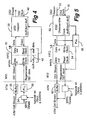
- Figure 4 illustrates a functional block diagram in the Tx direction of a typical DS1/DS2 multiplexer (often called M12 multiplexer).
- M12 multiplexer the service clock of each lower rate signal stream must be recovered in relation to the network reference clock and then each lower rate signal must be rate adjusted to be synchronous with each other by appropriate stuffing. Therefore in Figure 4, ATM cells from the network are buffered at buffer 30 and a DS1 signal stream is fed to a FIFO 32. Meanwhile, SRTS values are captured from the ATM cell stream. They are then processed at 34 by referring to the network reference clock, e.g., 2.430MHz and a DS1 clock is regenerated through PLL 36.
- the network reference clock e.g., 2.430MHz
- the incoming DS1 signal stream is written in in response to the regenerated DS1 clock.
- DS1 signal stream stored in the FIFO are read out and sent to DS2 mapper 38 in accordance with the clock signal obtained from DS2 clock 40.
- the DS2 mapper will stuff in DS1 data into the stuff position.
- the rate at which the FIFO is emptied increases and eventually the fullness of the FIFO will drop below a threshold 42 and the DS2 mapper will then put nulls into the stuff position.
- DS2 mapper maps four DS1 signal streams into a DS2 signal stream.
- FIG. 5 illustrates a functional block diagram in the Rx direction of a known M12 multiplexer.
- a DS2 signal stream 50 is disassembled at a disassembler 52 to DS1 signal streams, each DS1 signal stream properly destuffed.
- Each DS1 signal stream is sent and stored in FIFO 54 according to write clock derived from DS2 clock 56.
- Each DS1 stream is read out from the FIFO according to a regenerated clock for the respective DS1 stream.
- the respective clock is regenerated from the data bits coming out of the disassembler and the stuff/don't stuff signal through a PLL 58.
- the data is read out of the FIFO in accordance with this recovered clock and stored in the ATM cell buffer 60.
- SRTS values are calculated at 62 with respect to the network reference clock and inserted into the appropriate places in the ATM cells as they are sent to the ATM network.
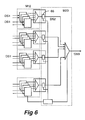
- DS1 signal streams are multiplexed into a DS3 signal stream at the same location. As shown in Figure 6, this is performed by a series of M12 and M23 multiplexing. In the Figure, seven M12, each with an appropriate stuffing operation at 66 are combined to generate a DS3 signal stream. Some stuffing determination based on various means is performed here.
- the SRTS clock recovery techniques discussed above deal mainly regenerating a digital signal e.g. DS1 signal which is already fairly narrowly bounded. These techniques therefore do not have a sufficient dynamic range to deal with multiplexing and demultiplexing of DS1 and DS3 streams.
- the multiplexer/demultiplexer of the invention makes use of the SRTS technique but it is entirely digital in operation. It also handles digital signal streams of wider hierarchies, such as signals spanning between DS1 and DS3. As the operation is entirely digital, the technique of context switching can also be applied to it.
- the contents of the various registers that make up the inventive algorithm are stored in a memory for each of the 28 DS1 signal streams. As each DS1 signal stream is processed, the values for the registers are loaded from the memory, the registers are updated appropriately, and the new values stored back into memory.
- the algorithm completely digital one avoids an analog PLL, the device pins that it needs, as well as any external components that a PLL may require for each of the 28 DS1 signal stream.
- context switching allows a single set of hardware registers along with a memory to replace 28 sets of the DS1 hardware registers which would be required for the prior art techniques mentioned above. It is therefore possible to achieve significantly higher levels of integration.
- US Patent Serial No.5,563,891 discloses multiplexing a plurality of first signal streams into a higher rate second stream by buffering and stuffing the first signal streams before combining with the second stream.
- a demultiplexer for demultiplexing a first signal stream having a first rate into a plurality of second signal streams, each having a substantially similar rate that is lower than the first rate, characterized by: a disassembling circuit for disassembling the first signal stream into the plurality of second signal streams, an incoming SRTS circuit for generating an incoming SRTS value for each of the second signal streams; an SRTS block for generating an outgoing SRTS value for each of the second signal streams in response to a difference between the incoming and outgoing SRTS values; and an inserting circuit for inserting the outgoing SRTS value in each respective second signal stream.
- the incoming SRTS circuit may comprise incoming delta circuits for calculating a first difference of successive incoming SRTS values; and the SRTS block may comprise outgoing delta circuits for calculating a second difference of successive outgoing SRTS values, and a cumulative delta circuit for registering a cumulative value of a third difference between the first and second differences for each second signal stream.
- the demultiplexer may include a memory for storing instantiation values of the incoming SRTS circuit and SRTS block for each second signal stream, and a processor for context switching algorithm executions of the incoming SRTS circuit, SRTS block and the inserting circuit for each second signal stream.
- the SRTS block preferably comprises a stuff target circuit for comparing the cumulative value of the third difference and a target SRTS value to generate the outgoing SRTS value.
- an SRTS value is generated for each first signal stream, a local SRTS value is generated based on the second rate of the second signal stream, and from the received SRTS value and the generated local SRTS value is calculated a difference indication proportional to the difference between the first and the second rates.
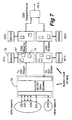
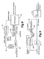
- FIG. 7 is a functional block diagram of DS1-DS3 multiplexer/demultiplexer according to one embodiment related to the invention.
- DS1 or DS0 signal streams are received from or sent to an ATM network or some other network and multiplexed into or demultiplexed from a DS3 signal stream.
- An interface arrangement 70 produces an octet stream of 28 DS1 signal streams in the Tx direction and receive them in the Rx direction.
- Each of 28 DS1 signal streams is processed by M12 mux which contains various sets of algorithms 72 and 74, e.g., a framing algorithm, SRTS algorithm, stuffing algorithm etc.
- the SRTS and stuffing algorithms will be described in detail below.
- each of 28 DS1 signal streams is executed by context switching in co-operation with a memory 76 and therefore the output of M12 is seven DS 2 signal streams.
- Each of seven DS2 signal streams is processed by multiplexer M23 which, like M12, contains necessary algorithms and executed by context switching. Seven DS2 signal streams are then combined and mapped onto a properly framed DS3 signal stream. In the Rx direction, a DS3 signal stream is processed by similar algorithms at M23 and M12. At M12, rate adjustment is performed by SRTS and stuffing algorithms, which will be described in detail below also.
- FIG 8 is a functional block diagram of a multiplexer of DS1 signal streams to a DS2 signal stream, containing an embodiment of the invention.
- each of a plurality (e.g. 28) of DS1 signal streams is buffered at FIFO 80 and its SRTS value is recovered by a SRTS recovery buffer 82.
- This sequence of SRTS values is an indication of the rate of an incoming DS1 signal stream.
- a DS2 mapper 84 reads a DS1 stream stored in the FIFO. Having appropriately rate adjusted by stuffing, the DS2 mapper maps four DS1 signal streams into an outgoing DS2 signal stream. The stuffing action as well as DS2 framing takes place in the mapper 84.
- SRTS Block 90 Decision to stuff the stuff position with a null bit or data bit is performed at SRTS Block 90. Therefore, a counter reads DS1 bits of a particular DS1 signal stream which is mapped to the DS2 signal stream. The counter performs a division by 3008 and latches the clock count of a network reference clock, e.g., 2.430MHz. The content of the latch is the local SRTS value which is an indication of the rate of the particular outgoing DS1 stream multiplexed into the DS2 stream.
- the SRTS Block 90 compares the sequence of the recovered SRTS values and the sequence of local SRTS values and generates a command of stuff null or stuff data at a stuff position with respect to each of the 28 DS1 signal streams.
- each DS2 signal stream is further stuffed while a DS3 mapper maps seven DS2 signal streams into a DS3 signal stream. Seven DS2 signal streams are individually stuffed to align all the DS2 signal streams.
- FIG 9 is a functional block diagram of a demultiplexer of a DS2 signal stream to DS1 signal streams, containing an embodiment related to the invention.
- each of seven DS2 signal streams is demultiplexed into 4 DS1 signal streams at disassembler 92.
- Each of a plurality of DS1 signal streams is buffered in a FIFO 94.
- a counter 96 counts the DS1 bits for a particular DS1 signal stream taking into account the presence or absence of a data bit in each stuff opportunity.
- the counter divides by 3008 and latches at latch 98 the clock count of a network reference clock, e.g., 2.430MHz.
- the content of the latch is the incoming SRTS value, the sequence of which is an indication of the rate of the particular incoming DS1 stream.
- the SRTS block 100 generates an outgoing SRTS value, the sequence of which is an indication of the rate of a particular outgoing DS1 stream.
- the SRTS block compares the incoming SRTS sequence and the outgoing SRTS sequence and alters the outgoing SRTS sequence so that the outgoing rate for a particular DS1 signal stream will match the incoming rate for that DS1 signal stream.
- This SRTS sequence is embedded in each respective DS1 stream.
- SRTS block 90 of Figure 8 consists of two parts. The first is used to define a stuffing ratio required to align the incoming data rate as defined by the sequence of incoming SRTS values and the outgoing data rate as defined by the sequence of local SRTS values. The second part produces a sequence of stuff values corresponding to the stuffing ratio determined above, which controls the outgoing data rate and feeds this back to the first section.
- the transmit DS3 channel is driven by a TX clock rate and it is necessary to provide a data bit for each TX clock.
- Each data bit may correspond to a DS3 frame bit or one of the seven DS2 channels (for which it may be a data bit or a stuff bit).
- each bit for a DS2 channel may correspond to a frame bit or one of the 28 DS1 channels where it too may be a data bit or a stuff bit.
- the process for data rate alignment is triggered by the request to send DS1 bits.
- a new local SRTS value is computed and a new incoming SRTS value is read.
- the difference between successive local SRTS values is computed and is an indication of the clock rate for the outgoing DS1 bits.
- the difference between incoming SRTS values is calculated and is an indication of the clock rate of the incoming DS1 data stream. The difference between these differences is a measure of how far apart the incoming and outgoing clock rates are.
- the circuit then accumulates the difference of differences and attempts to adjust the outgoing SRTS rate so that the cumulative difference is zero thereby ensuring that the two frequencies are in alignment.
- the local delta SRTS values will be varying considerably, whereas the outgoing delta SRTS values will be smoothed to a roughly constant value.
- the outgoing DS1 data rate can be controlled by altering the stuffing ratio that is used.
- the stuffing ratio that is used.
- Part one of the invention above determines the data rate of the outgoing data stream. This data rate is expressed as a desired stuffing ratio that will range between 0 and 100%. Whatever the stuffing ratio is, part two of the invention produces a sequence of stuff/don't stuff signals that will correspond to the desired stuffing ratio.
- the correct sequence of stuff/don't stuff signals for this data rate is then: 110110110... where 1 means that a data bit is added and 0 means that a null bit is added.
- the stuffing ratio In order to generate a sequence of 0s and 1 s that average out to the desired stuffing ratio, one represents the stuffing ratio as a ratio between an N bit target value and an N bit denominator, i.e., target/2 N . With this representation, the stuffing ratio can range from 0 to (2 N - 1)/(2 N ). If the target value is summed 2 N times, then the total will be (2 N )*target. If the sum is computed modulo 2 N , and a 1 selected whenever the sum is 2 N or greater and 0 whenever the sum is less than 2 N , then after 2 N samples a 1 will be produced exactly target times and a 0 ⁇ (2 N )-target ⁇ times. The average value will be exactly that required, namely target/(2 N ), and the sequence of ones and zeros will be distributed as evenly as possible, thereby minimizing the error of the average stuffing ratio with respect to the desired stuffing ratio.
- the outgoing and incoming clock rates may differ which will lead to a drift in the respective SRTS differences.
- the target value will be adjusted by one thereby causing the outgoing clock rate to change so that the differences will drift in the opposite direction. This will continue indefinitely with the average of the two target values reflecting the true incoming clock rate.
- SRTS block 100 of Figure 9 consists also of two parts. These functions are almost identical to those used for multiplexer. Like multiplexer, the first is used to define a target delta SRTS value required to align the incoming data rate as defined by the sequence of incoming SRTS values and the outgoing data rate as defined by the sequence of outgoing SRTS values. The second part produces a sequence of SRTS values whose difference corresponds to the target delta SRTS value determined above, which controls the outgoing data rate and feeds this back to the first section.
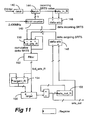
- SRTS logic block 90 of Figure 8 for Tx direction and SRTS logic block 100 of Figure 9 for Rx direction are described below in more detail in connection with one embodiment of the invention.
- an incoming SRTS value from the network is 4 bits wide which is converted to 5 bits wide at 110.
- a DS1 stream (DS1 bit) is divided by 3008 which then causes the 5 bit counter of the network reference clock to be latched at latch 112.
- the content of the latch is the local SRTS value.
- Delta local SRTS is a difference between successive local SRTS values and is calculated at delta_srts 114.
- delta incoming SRTS is a difference between successive incoming SRTS values and is calculated at delta_srts 116.
- a difference between two deltas, delta local SRTS and delta incoming SRTS, is accumulated at 118 which produces cumulative delta SRTS, cd_srts_R.
- the cumulative delta SRTS is then filtered at 120 to help remove the jitter due to the framing formats, DS2 and DS3 jitter in addition to source jitter and SRTS variability.
- fcd_srts_R a filtered cumulative delta SRTS value that is controlled so that the filtered cumulative delta SRTS value tends to zero.
- the stuffing sequence generator, 126 will produce a sequence of stuff null and stuff data that averages out to the ratio specified by the stuffing target.
- a DS1 stream (DS1 bit) 140 from the demultiplexer is divided by 3008 which then causes the 5 bit counter 142 of the network reference clock to be latched at latch 144.
- the content of the latch represents the incoming SRTS value.
- a difference between successive incoming SRTS values is computed at delta_srts 146.
- a difference of successive outgoing SRTS values is computed at delta_srts 148 and converted to a 5 bit value.
- Another difference of these two deltas is computed and accumulated at cd_srts_R 150. This is the cumulative delta SRTS value.
- This value is then filtered at 152 to remove jitter due to the framing formats, DS2 and DS3 jitter in addition to source jitter and outgoing SRTS variability.
- fcd_srts_R filtered cumulative delta SRTS value
- the contents of the various registers that make up the algorithm are stored in a memory for each of the 28 DS1 s.
- the values for the registers are loaded from the memory, the registers are updated appropriately, and the new values stored back into memory.
- context switching allows a single set of hardware registers along with a memory can replace 28 sets of the DS1 hardware registers which would be required for the prior art techniques mentioned above. It is therefore possible to achieve much higher levels of integration.
Landscapes
- Engineering & Computer Science (AREA)
- Signal Processing (AREA)
- Computer Networks & Wireless Communication (AREA)
- Multimedia (AREA)
- Computer Hardware Design (AREA)
- Time-Division Multiplex Systems (AREA)
- Data Exchanges In Wide-Area Networks (AREA)
Claims (5)
- Démultiplexeur destiné à démultiplexer un premier flux de signal comprenant une première fréquence en une pluralité de seconds flux de signal, chacun ayant une fréquence sensiblement similaire qui est inférieure à la première fréquence, comprenant :un circuit de désassemblage (92) destiné à désassembler le premier flux de signal en la pluralité de seconds flux de signal, et caractérisé par :un circuit de SRTS entrant (96, 98) destiné à générer une valeur de SRTS entrante pour chacun des seconds flux de signal ;un bloc de SRTS (100) destiné à générer une valeur de SRTS sortante pour chacun des seconds flux de signal en réponse à une différence entre les valeurs de SRTS entrantes et sortantes ; etun circuit d'insertion destiné à insérer la valeur de SRTS sortante dans chaque second flux de signal respectif.
- Démultiplexeur selon la revendication 1, dans lequel :le circuit de SRTS entrant comprend des circuits delta entrants (146) destinés à calculer une première différence des valeurs de SRTS entrantes successives ; et le bloc de SRTS comprend des circuits delta sortants (148) destinés à calculer une seconde différence des valeurs de SRTS sortantes successives et un circuit delta cumulatif (150) destiné à enregistrer une valeur cumulative d'une troisième différence entre la première et la seconde différences pour chaque second flux de signal.
- Démultiplexeur selon la revendication 2, comprenant également :une mémoire destinée à enregistrer les valeurs d'instanciation du circuit SRTS entrant et du bloc de SRTS pour chaque second flux de signal ; etun processeur destiné à réaliser les exécutions des algorithmes de commutation de contexte.
- Démultiplexeur selon la revendication 2 ou la revendication 3, dans lequel le bloc de SRTS comprend :un circuit de cible de justification (156) destiné à comparer la valeur cumulative de la troisième différence et une valeur de SRTS cible pour générer la valeur de SRTS sortante.
- Démultiplexeur selon l'une quelconque des revendications 1 à 4 dans lequel le premier et le second flux de signal sont choisis parmi un groupe quelconque des suivants : DS1, DS2, et DS3, et E1, E2 et E3.
Applications Claiming Priority (3)
| Application Number | Priority Date | Filing Date | Title |
|---|---|---|---|
| US08/995,414 US6157659A (en) | 1997-12-19 | 1997-12-19 | Method of and apparatus for multiplexing and demultiplexing digital signal streams |
| US995414 | 1997-12-19 | ||
| EP98310079A EP0926851B1 (fr) | 1997-12-19 | 1998-12-09 | Méthode et dispositif de multiplexage et demultiplexage de trains de signaux numériques |
Related Parent Applications (1)
| Application Number | Title | Priority Date | Filing Date |
|---|---|---|---|
| EP98310079A Division EP0926851B1 (fr) | 1997-12-19 | 1998-12-09 | Méthode et dispositif de multiplexage et demultiplexage de trains de signaux numériques |
Publications (2)
| Publication Number | Publication Date |
|---|---|
| EP1585243A1 EP1585243A1 (fr) | 2005-10-12 |
| EP1585243B1 true EP1585243B1 (fr) | 2006-10-11 |
Family
ID=25541755
Family Applications (2)
| Application Number | Title | Priority Date | Filing Date |
|---|---|---|---|
| EP98310079A Expired - Lifetime EP0926851B1 (fr) | 1997-12-19 | 1998-12-09 | Méthode et dispositif de multiplexage et demultiplexage de trains de signaux numériques |
| EP05270025A Expired - Lifetime EP1585243B1 (fr) | 1997-12-19 | 1998-12-09 | Méthode et dispositif de demultiplexage de trains de signaux numériques |
Family Applications Before (1)
| Application Number | Title | Priority Date | Filing Date |
|---|---|---|---|
| EP98310079A Expired - Lifetime EP0926851B1 (fr) | 1997-12-19 | 1998-12-09 | Méthode et dispositif de multiplexage et demultiplexage de trains de signaux numériques |
Country Status (6)
| Country | Link |
|---|---|
| US (1) | US6157659A (fr) |
| EP (2) | EP0926851B1 (fr) |
| JP (1) | JP3330888B2 (fr) |
| KR (1) | KR19990063234A (fr) |
| CA (1) | CA2254591C (fr) |
| DE (2) | DE69836157T2 (fr) |
Families Citing this family (49)
| Publication number | Priority date | Publication date | Assignee | Title |
|---|---|---|---|---|
| US6765928B1 (en) | 1998-09-02 | 2004-07-20 | Cisco Technology, Inc. | Method and apparatus for transceiving multiple services data simultaneously over SONET/SDH |
| KR100276609B1 (ko) * | 1998-10-29 | 2001-01-15 | 서평원 | 디에스3 프레임 구조 및 이를 이용한 디지털 티브이 신호의 전송장치 |
| US6751228B1 (en) * | 1999-03-23 | 2004-06-15 | Yamaha Corporation | Packet handler of audio data by isochronous mode |
| CA2442597C (fr) | 2000-03-27 | 2011-11-01 | Transcept Opencell, Inc. | Architecture de systeme sans fil reparti multi-protocole |
| DE10029063A1 (de) | 2000-06-13 | 2002-01-03 | Siemens Ag | Verfahren und Anordnung zur Übertragung von mindestens einem Clientsignal innerhalb eines Serversignales |
| US6801539B1 (en) * | 2000-06-26 | 2004-10-05 | Adtran, Inc. | Serialized HDSL multiplexer - demultiplexer protocol |
| US6704545B1 (en) | 2000-07-19 | 2004-03-09 | Adc Telecommunications, Inc. | Point-to-multipoint digital radio frequency transport |
| US7346698B2 (en) * | 2000-12-20 | 2008-03-18 | G. W. Hannaway & Associates | Webcasting method and system for time-based synchronization of multiple, independent media streams |
| US20020163930A1 (en) * | 2001-02-28 | 2002-11-07 | Phillip Kreider | Methods and systems for interleaving data from multi-rate channels into a single interface |
| WO2003019873A1 (fr) * | 2001-08-22 | 2003-03-06 | Tekelec | Procedes et systemes d'amelioration de l'utilisation de liaisons de communication haute vitesse multiplexees par repartition dans le temps dans un point de transfert de signaux |
| SG102012A1 (en) * | 2001-11-07 | 2004-02-27 | Agilent Technologies Inc | Gigabit ethernet bridge with parallel fifo structure |
| KR100464370B1 (ko) | 2002-02-22 | 2005-01-03 | 삼성전자주식회사 | 라인 인터페이스 장치에서 전송 모드 자동 설정 방법 |
| US7184728B2 (en) | 2002-02-25 | 2007-02-27 | Adc Telecommunications, Inc. | Distributed automatic gain control system |
| US7308004B1 (en) | 2002-03-06 | 2007-12-11 | Redback Networks, Inc. | Method and apparatus of multiplexing and demultiplexing communication signals |
| US6831901B2 (en) * | 2002-05-31 | 2004-12-14 | Opencell Corporation | System and method for retransmission of data |
| US8958789B2 (en) | 2002-12-03 | 2015-02-17 | Adc Telecommunications, Inc. | Distributed digital antenna system |
| EP1455472A1 (fr) * | 2003-03-07 | 2004-09-08 | STMicroelectronics Limited | Control de synchronisation pour flots de paquets |
| US20050036522A1 (en) * | 2003-08-15 | 2005-02-17 | Adc Dsl Systems, Inc. | Multiplexers in a synchronous optical network |
| US7031256B2 (en) * | 2004-01-20 | 2006-04-18 | Transwitch Corporation | Methods and apparatus for implementing LCAS ( link capacity adjustment scheme) sinking with rate based flow control |
| US7787854B2 (en) * | 2005-02-01 | 2010-08-31 | Adc Telecommunications, Inc. | Scalable distributed radio network |
| US7484160B2 (en) * | 2005-03-04 | 2009-01-27 | Tellabs Operations, Inc. | Systems and methods for delineating a cell in a communications network |
| US20070008939A1 (en) * | 2005-06-10 | 2007-01-11 | Adc Telecommunications, Inc. | Providing wireless coverage into substantially closed environments |
| US9544638B2 (en) * | 2006-04-17 | 2017-01-10 | Broadcom Corporation | Method for reconstructing system time clock (STC) without carrying PCR |
| US7805073B2 (en) | 2006-04-28 | 2010-09-28 | Adc Telecommunications, Inc. | Systems and methods of optical path protection for distributed antenna systems |
| US7844273B2 (en) * | 2006-07-14 | 2010-11-30 | Lgc Wireless, Inc. | System for and method of for providing dedicated capacity in a cellular network |
| US7848770B2 (en) | 2006-08-29 | 2010-12-07 | Lgc Wireless, Inc. | Distributed antenna communications system and methods of implementing thereof |
| FI122670B (fi) * | 2006-09-15 | 2012-05-15 | Tellabs Oy | Menetelmä ja järjestely datakehysten välisen aikajakson tuottamiseksi |
| US7817958B2 (en) | 2006-12-22 | 2010-10-19 | Lgc Wireless Inc. | System for and method of providing remote coverage area for wireless communications |
| US8737454B2 (en) | 2007-01-25 | 2014-05-27 | Adc Telecommunications, Inc. | Modular wireless communications platform |
| US8583100B2 (en) | 2007-01-25 | 2013-11-12 | Adc Telecommunications, Inc. | Distributed remote base station system |
| US8005050B2 (en) | 2007-03-23 | 2011-08-23 | Lgc Wireless, Inc. | Localization of a mobile device in distributed antenna communications system |
| US20080236393A1 (en) * | 2007-03-28 | 2008-10-02 | Adc Dsl Systems, Inc. | Filter assembly |
| US20080240090A1 (en) * | 2007-03-28 | 2008-10-02 | Adc Dsl Systems, Inc. | Programmable high speed crossbar switch |
| US8010116B2 (en) | 2007-06-26 | 2011-08-30 | Lgc Wireless, Inc. | Distributed antenna communications system |
| US9112547B2 (en) | 2007-08-31 | 2015-08-18 | Adc Telecommunications, Inc. | System for and method of configuring distributed antenna communications system |
| US8310963B2 (en) * | 2008-06-24 | 2012-11-13 | Adc Telecommunications, Inc. | System and method for synchronized time-division duplex signal switching |
| US9001811B2 (en) | 2009-05-19 | 2015-04-07 | Adc Telecommunications, Inc. | Method of inserting CDMA beacon pilots in output of distributed remote antenna nodes |
| US8472579B2 (en) | 2010-07-28 | 2013-06-25 | Adc Telecommunications, Inc. | Distributed digital reference clock |
| CN101951304B (zh) * | 2010-08-31 | 2012-04-18 | 华为技术有限公司 | 微波传输装置 |
| US8532242B2 (en) | 2010-10-27 | 2013-09-10 | Adc Telecommunications, Inc. | Distributed antenna system with combination of both all digital transport and hybrid digital/analog transport |
| US8462683B2 (en) | 2011-01-12 | 2013-06-11 | Adc Telecommunications, Inc. | Distinct transport path for MIMO transmissions in distributed antenna systems |
| US8693342B2 (en) | 2011-10-28 | 2014-04-08 | Adc Telecommunications, Inc. | Distributed antenna system using time division duplexing scheme |
| RU2514092C2 (ru) * | 2012-03-30 | 2014-04-27 | Федеральное государственное унитарное предприятие "Ростовский-на-Дону научно-исследовательский институт радиосвязи" (ФГУП "РНИИРС") | Способ и устройство синхронизации и демультиплексирования компонентных сигналов в цифровых потоках |
| CN110212974B (zh) | 2013-02-22 | 2022-10-04 | Adc电信股份有限公司 | 来自于分布式天线系统的基站网络接口的主基准 |
| KR102228617B1 (ko) | 2013-02-22 | 2021-03-15 | 콤스코프 테크놀로지스 엘엘씨 | 범용 원격 라디오 헤드 |
| US9787457B2 (en) | 2013-10-07 | 2017-10-10 | Commscope Technologies Llc | Systems and methods for integrating asynchronous signals in distributed antenna system with direct digital interface to base station |
| EP3108627A4 (fr) | 2014-02-18 | 2017-10-11 | CommScope Technologies LLC | Combinaison sélective de signaux en liaison montante dans des systèmes d'antennes distribués |
| AU2015274498B2 (en) | 2014-06-11 | 2019-09-19 | Commscope Technologies Llc | Bitrate efficient transport through distributed antenna systems |
| US10499269B2 (en) | 2015-11-12 | 2019-12-03 | Commscope Technologies Llc | Systems and methods for assigning controlled nodes to channel interfaces of a controller |
Family Cites Families (10)
| Publication number | Priority date | Publication date | Assignee | Title |
|---|---|---|---|---|
| US4961188A (en) * | 1989-09-07 | 1990-10-02 | Bell Communications Research, Inc. | Synchronous frequency encoding technique for clock timing recovery in a broadband network |
| US5260978A (en) * | 1992-10-30 | 1993-11-09 | Bell Communications Research, Inc. | Synchronous residual time stamp for timing recovery in a broadband network |
| US5526362A (en) * | 1994-03-31 | 1996-06-11 | Telco Systems, Inc. | Control of receiver station timing for time-stamped data |
| GB9419611D0 (en) * | 1994-09-29 | 1994-11-16 | Plessey Telecomm | Constant bit rate synchronisation |
| US5608731A (en) * | 1995-03-31 | 1997-03-04 | Transwitch Corporation | Closed loop clock recovery for synchronous residual time stamp |
| US5563891A (en) * | 1995-09-05 | 1996-10-08 | Industrial Technology Research Institute | Waiting time jitter reduction by synchronizer stuffing threshold modulation |
| US5822383A (en) * | 1995-12-15 | 1998-10-13 | Cisco Technology, Inc. | System and method for maintaining network synchronization utilizing digital phase comparison techniques with synchronous residual time stamps |
| US5825770A (en) * | 1996-06-06 | 1998-10-20 | Northern Telecom Limited | Multiple algorithm processing on a plurality of digital signal streams via context switching |
| JP3011128B2 (ja) * | 1997-03-28 | 2000-02-21 | 日本電気株式会社 | Aalタイプ1伝送におけるクロック情報転送方式 |
| EP0876017A1 (fr) * | 1997-05-02 | 1998-11-04 | Lsi Logic Corporation | Système numérique de récupération d'horloge |
-
1997
- 1997-12-19 US US08/995,414 patent/US6157659A/en not_active Expired - Fee Related
-
1998
- 1998-11-26 CA CA002254591A patent/CA2254591C/fr not_active Expired - Lifetime
- 1998-12-09 DE DE69836157T patent/DE69836157T2/de not_active Expired - Lifetime
- 1998-12-09 DE DE69831473T patent/DE69831473T2/de not_active Expired - Lifetime
- 1998-12-09 EP EP98310079A patent/EP0926851B1/fr not_active Expired - Lifetime
- 1998-12-09 JP JP35016898A patent/JP3330888B2/ja not_active Expired - Fee Related
- 1998-12-09 EP EP05270025A patent/EP1585243B1/fr not_active Expired - Lifetime
- 1998-12-18 KR KR1019980056331A patent/KR19990063234A/ko not_active Application Discontinuation
Also Published As
| Publication number | Publication date |
|---|---|
| EP0926851B1 (fr) | 2005-09-07 |
| EP0926851A3 (fr) | 2003-04-02 |
| DE69831473D1 (de) | 2005-10-13 |
| US6157659A (en) | 2000-12-05 |
| JP3330888B2 (ja) | 2002-09-30 |
| DE69831473T2 (de) | 2006-02-02 |
| EP0926851A2 (fr) | 1999-06-30 |
| KR19990063234A (ko) | 1999-07-26 |
| EP1585243A1 (fr) | 2005-10-12 |
| DE69836157T2 (de) | 2007-01-18 |
| CA2254591A1 (fr) | 1999-06-19 |
| JPH11252034A (ja) | 1999-09-17 |
| DE69836157D1 (de) | 2006-11-23 |
| CA2254591C (fr) | 2002-06-04 |
Similar Documents
| Publication | Publication Date | Title |
|---|---|---|
| EP1585243B1 (fr) | Méthode et dispositif de demultiplexage de trains de signaux numériques | |
| US6188693B1 (en) | ATM multiplexing apparatus, ATM demultiplexing apparatus, and communication network with the apparatus | |
| US5263057A (en) | Method of reducing waiting time jitter | |
| US6415006B2 (en) | Reducing waiting time jitter | |
| CN114830593B (zh) | 通过分组传送网络传送恒定比特率客户端信号的系统和方法 | |
| US6456678B2 (en) | Elastic store for wireless communication systems | |
| US6714548B2 (en) | Digital clock recovery | |
| US7457390B2 (en) | Timeshared jitter attenuator in multi-channel mapping applications | |
| US7639673B2 (en) | Method and apparatus for SDH/SONET frame alignment | |
| US6272138B1 (en) | Method and apparatus for reducing jitter or wander on internetworking between ATM network and PDH network | |
| US7940806B1 (en) | Synchronous payload envelope mapping without pointer adjustments | |
| EP0525770B1 (fr) | Procédé et dispositif pour renouveler des pointeurs AU-4 et TU-3 de la hiérarchie numérique synchrone | |
| US7443888B2 (en) | Transparent sub-wavelength network | |
| JP3398593B2 (ja) | ペイロード相対位置変更要求装置及びそれを含む伝送装置 | |
| US7590154B2 (en) | Sampled accumulation system and method for jitter attenuation | |
| JP2952935B2 (ja) | 非同期データ伝送システム | |
| US7349444B2 (en) | SONET/SDH SPE/virtual container retiming with adaptive dual pointer leak rate computation | |
| US5883900A (en) | Telecommunications transmission | |
| JPH053463A (ja) | スタツフ多重通信受信回路 | |
| EP0674407B1 (fr) | Justification complémentaire | |
| KR0153953B1 (ko) | 고정 비트율 서비스에서 보조 잔류 타임 스템프 값을 이용한 클럭 복원 장치 | |
| KR20040057018A (ko) | 동기식 다중화기의 동기장치 | |
| KR20010113421A (ko) | 개선된 포인터 조정 동기 장치 | |
| JPH07162433A (ja) | 速度変換方式 |
Legal Events
| Date | Code | Title | Description |
|---|---|---|---|
| PUAI | Public reference made under article 153(3) epc to a published international application that has entered the european phase |
Free format text: ORIGINAL CODE: 0009012 |
|
| 17P | Request for examination filed |
Effective date: 20050722 |
|
| AC | Divisional application: reference to earlier application |
Ref document number: 0926851 Country of ref document: EP Kind code of ref document: P |
|
| AK | Designated contracting states |
Kind code of ref document: A1 Designated state(s): AT BE BG CH CY CZ DE DK EE ES FI FR GB GR HU IE IS IT LI LT LU MC NL PL PT RO SE SI SK TR |
|
| AX | Request for extension of the european patent |
Extension state: AL BA HR LV MK YU |
|
| GRAP | Despatch of communication of intention to grant a patent |
Free format text: ORIGINAL CODE: EPIDOSNIGR1 |
|
| AKX | Designation fees paid |
Designated state(s): DE FR GB |
|
| GRAS | Grant fee paid |
Free format text: ORIGINAL CODE: EPIDOSNIGR3 |
|
| GRAA | (expected) grant |
Free format text: ORIGINAL CODE: 0009210 |
|
| AC | Divisional application: reference to earlier application |
Ref document number: 0926851 Country of ref document: EP Kind code of ref document: P |
|
| AK | Designated contracting states |
Kind code of ref document: B1 Designated state(s): DE FR GB |
|
| REG | Reference to a national code |
Ref country code: GB Ref legal event code: FG4D |
|
| REF | Corresponds to: |
Ref document number: 69836157 Country of ref document: DE Date of ref document: 20061123 Kind code of ref document: P |
|
| ET | Fr: translation filed | ||
| PLBE | No opposition filed within time limit |
Free format text: ORIGINAL CODE: 0009261 |
|
| STAA | Information on the status of an ep patent application or granted ep patent |
Free format text: STATUS: NO OPPOSITION FILED WITHIN TIME LIMIT |
|
| 26N | No opposition filed |
Effective date: 20070712 |
|
| REG | Reference to a national code |
Ref country code: GB Ref legal event code: 732E Free format text: REGISTERED BETWEEN 20101230 AND 20110105 |
|
| REG | Reference to a national code |
Ref country code: FR Ref legal event code: TP |
|
| REG | Reference to a national code |
Ref country code: DE Ref legal event code: R082 Ref document number: 69836157 Country of ref document: DE Representative=s name: PATENTANWAELTE WALLACH, KOCH & PARTNER, DE |
|
| REG | Reference to a national code |
Ref country code: DE Ref legal event code: R081 Ref document number: 69836157 Country of ref document: DE Owner name: CIENA LUXEMBOURG S.A.R.L., LU Free format text: FORMER OWNER: NORTEL NETWORKS LTD., ST. LAURENT, QUEBEC, CA Effective date: 20120213 Ref country code: DE Ref legal event code: R082 Ref document number: 69836157 Country of ref document: DE Representative=s name: PATENTANWAELTE WALLACH, KOCH & PARTNER, DE Effective date: 20120213 Ref country code: DE Ref legal event code: R082 Ref document number: 69836157 Country of ref document: DE Representative=s name: PATENTANWAELTE WALLACH, KOCH, DR. HAIBACH, FEL, DE Effective date: 20120213 |
|
| REG | Reference to a national code |
Ref country code: FR Ref legal event code: PLFP Year of fee payment: 18 |
|
| REG | Reference to a national code |
Ref country code: FR Ref legal event code: PLFP Year of fee payment: 19 |
|
| REG | Reference to a national code |
Ref country code: FR Ref legal event code: PLFP Year of fee payment: 20 |
|
| PGFP | Annual fee paid to national office [announced via postgrant information from national office to epo] |
Ref country code: DE Payment date: 20171211 Year of fee payment: 20 Ref country code: FR Payment date: 20171221 Year of fee payment: 20 |
|
| PGFP | Annual fee paid to national office [announced via postgrant information from national office to epo] |
Ref country code: GB Payment date: 20171221 Year of fee payment: 20 |
|
| REG | Reference to a national code |
Ref country code: DE Ref legal event code: R071 Ref document number: 69836157 Country of ref document: DE |
|
| REG | Reference to a national code |
Ref country code: GB Ref legal event code: PE20 Expiry date: 20181208 |
|
| PG25 | Lapsed in a contracting state [announced via postgrant information from national office to epo] |
Ref country code: GB Free format text: LAPSE BECAUSE OF EXPIRATION OF PROTECTION Effective date: 20181208 |