EP1585161A2 - Plasmaanzeigetafel - Google Patents
Plasmaanzeigetafel Download PDFInfo
- Publication number
- EP1585161A2 EP1585161A2 EP05102835A EP05102835A EP1585161A2 EP 1585161 A2 EP1585161 A2 EP 1585161A2 EP 05102835 A EP05102835 A EP 05102835A EP 05102835 A EP05102835 A EP 05102835A EP 1585161 A2 EP1585161 A2 EP 1585161A2
- Authority
- EP
- European Patent Office
- Prior art keywords
- display panel
- plasma display
- discharge
- upper substrate
- electrodes
- Prior art date
- Legal status (The legal status is an assumption and is not a legal conclusion. Google has not performed a legal analysis and makes no representation as to the accuracy of the status listed.)
- Withdrawn
Links
Images


Classifications
-
- H—ELECTRICITY
- H01—ELECTRIC ELEMENTS
- H01J—ELECTRIC DISCHARGE TUBES OR DISCHARGE LAMPS
- H01J11/00—Gas-filled discharge tubes with alternating current induction of the discharge, e.g. alternating current plasma display panels [AC-PDP]; Gas-filled discharge tubes without any main electrode inside the vessel; Gas-filled discharge tubes with at least one main electrode outside the vessel
- H01J11/20—Constructional details
- H01J11/34—Vessels, containers or parts thereof, e.g. substrates
- H01J11/44—Optical arrangements or shielding arrangements, e.g. filters, black matrices, light reflecting means or electromagnetic shielding means
-
- H—ELECTRICITY
- H04—ELECTRIC COMMUNICATION TECHNIQUE
- H04M—TELEPHONIC COMMUNICATION
- H04M1/00—Substation equipment, e.g. for use by subscribers
- H04M1/02—Constructional features of telephone sets
- H04M1/23—Construction or mounting of dials or of equivalent devices; Means for facilitating the use thereof
-
- H—ELECTRICITY
- H01—ELECTRIC ELEMENTS
- H01H—ELECTRIC SWITCHES; RELAYS; SELECTORS; EMERGENCY PROTECTIVE DEVICES
- H01H13/00—Switches having rectilinearly-movable operating part or parts adapted for pushing or pulling in one direction only, e.g. push-button switch
- H01H13/70—Switches having rectilinearly-movable operating part or parts adapted for pushing or pulling in one direction only, e.g. push-button switch having a plurality of operating members associated with different sets of contacts, e.g. keyboard
- H01H13/702—Switches having rectilinearly-movable operating part or parts adapted for pushing or pulling in one direction only, e.g. push-button switch having a plurality of operating members associated with different sets of contacts, e.g. keyboard with contacts carried by or formed from layers in a multilayer structure, e.g. membrane switches
- H01H13/704—Switches having rectilinearly-movable operating part or parts adapted for pushing or pulling in one direction only, e.g. push-button switch having a plurality of operating members associated with different sets of contacts, e.g. keyboard with contacts carried by or formed from layers in a multilayer structure, e.g. membrane switches characterised by the layers, e.g. by their material or structure
-
- H—ELECTRICITY
- H01—ELECTRIC ELEMENTS
- H01J—ELECTRIC DISCHARGE TUBES OR DISCHARGE LAMPS
- H01J11/00—Gas-filled discharge tubes with alternating current induction of the discharge, e.g. alternating current plasma display panels [AC-PDP]; Gas-filled discharge tubes without any main electrode inside the vessel; Gas-filled discharge tubes with at least one main electrode outside the vessel
- H01J11/10—AC-PDPs with at least one main electrode being out of contact with the plasma
- H01J11/12—AC-PDPs with at least one main electrode being out of contact with the plasma with main electrodes provided on both sides of the discharge space
-
- H—ELECTRICITY
- H01—ELECTRIC ELEMENTS
- H01J—ELECTRIC DISCHARGE TUBES OR DISCHARGE LAMPS
- H01J2211/00—Plasma display panels with alternate current induction of the discharge, e.g. AC-PDPs
- H01J2211/20—Constructional details
- H01J2211/34—Vessels, containers or parts thereof, e.g. substrates
- H01J2211/44—Optical arrangements or shielding arrangements, e.g. filters or lenses
- H01J2211/444—Means for improving contrast or colour purity, e.g. black matrix or light shielding means
Definitions
- the present invention relates to a plasma display panel comprising a discharge cell operable to emit light.
- a plasma display panel is an apparatus which forms an image using an electrical discharge.
- PDPs have superior performance in terms of brightness and viewing angle and are thus popular.
- DC or AC voltages applied to electrodes cause a gas discharge between the electrodes.
- Ultraviolet rays generated by the discharge excite a fluorescent material, which emits a visible light.
- PDPs are therefore classified as either DC or AC types depending on the voltage applied to the electrodes.
- the DC type PDP has a structure where all electrodes are exposed to the discharge space, and charges move directly between the electrodes.
- the AC type PDP has a structure where at least one electrode is covered with a dielectric layer so charges do not move directly between the corresponding electrodes but, instead, discharge is performed between wall charges.
- PDPs may be classified as a facing discharge type or a surface discharge type. This classification is dependent upon the arrangement of the electrodes.
- the facing discharge type PDP has a structure where a pair of sustain electrodes are formed respectively on an upper substrate and a lower substrate, and discharge occurs perpendicular to the substrate.
- the surface discharge type PDP has a structure where a pair of sustain electrodes are formed on the same substrate, and discharge occurs parallel to the substrate.
- the facing discharge type PDP has a high luminous efficiency, but a disadvantage in that the fluorescent layer is easily deteriorated. For this reason, the surface discharge type PDP is presently more common.
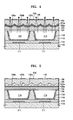
- Figures 1 and 2 show the construction of a known surface discharge type PDP.
- the upper substrate 20 is shown rotated by 90 degrees to aid understanding of the inner structure of the PDP.
- the known PDP includes a lower substrate 10 and an upper substrate 20 facing each other.
- a plurality of address electrodes 11 are arranged as stripes.
- the address electrodes 11 are covered by a first dielectric layer 12 (preferably white).
- a plurality of barrier ribs 13 having a predetermined spacing are formed. The space prevents electrical and optical cross-talk between discharge cells 14.
- a red (R), green (G) and blue (B) fluorescent layer 15 having a predetermined thickness is applied thereto.
- the discharge cells 14 are filled with a discharge gas, which is typically a mixture of neon (Ne) and a small amount of xenon (Xe). This is generally used for plasma discharge.
- the upper substrate 20 is a transparent substrate, which transmits visible light, and is preferably made of glass.
- the upper substrate 20 is coupled to the lower substrate 10.
- sustaining electrodes 21a and 21 b are formed in pairs and are formed perpendicular to the address electrodes 11.
- the sustaining electrodes 21a and 21b and are arranged as stripes.
- the sustaining electrodes 21a and 21b are formed of a transparent conductive material, such as indium tin oxide (ITO), which allows transmission of visible light.
- ITO indium tin oxide
- bus electrodes 22a and 22b are formed on the lower surface of the respective sustaining electrodes 21a and 21b.
- the bus electrodes 21a and 21b are made of a metal and have a width which is less than that of the sustaining electrodes 21a and 21b.
- the sustaining electrodes 21a and 21b and the bus electrodes 22a and 22b are covered with a transparent second dielectric layer 23.
- a protective layer 24 is formed on the lower surface of the second dielectric layer 23, a protective layer 24 is formed.
- the protective layer 24 prevents the second dielectric layer 23 from damage caused by plasma sputtering.
- the protective layer 24 emits secondary electrons which lower the discharge voltages.
- the protective layer 24 is generally formed of magnesium oxide (MgO).
- a plurality of black stripes 30 are formed at a predetermined spacing. The black stripes 30 are parallel to the sustaining electrodes 21a and 21b to prevent external light from entering the panel.
- the known PDP as above generally uses a cycle of two operations: address discharge and sustaining discharge.
- the address discharge occurs between the address electrode 11 and any one of the sustaining electrodes 21a and 21b.
- the sustaining discharge is caused by a potential difference between the sustaining electrodes 21a and 21 b positioned at the discharge cells 14 in which the wall charges are formed.
- the florescent layer 15 of the corresponding discharge cell is excited by ultraviolet rays generated from the discharge gas, thus emitting visible light.
- the visible light emitted through the upper substrate 20 forms the image on the PDP.
- the present invention provides a PDP with better brightness and bright room contrast by improving the structure of the upper substrate.
- the present invention relates to a plasma display panel comprising a discharge cell operable to emit light.
- a plasma display panel according to the present invention is characterised by a lenticular layer for focussing the light emitted by the cell, wherein the cell to lens ratio applicable to the cell is not 1:1.
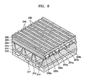
- the PDP comprises a lower substrate 110 and an upper substrate 120, which are spaced apart by a predetermined amount.
- the lower substrate 110 and the upper substrate 120 face each other.
- the space between the lower substrate 110 and the upper substrate 120 corresponds to a discharge space in which plasma discharge occurs.
- the lower substrate 110 is preferably formed of glass.
- a plurality of address electrodes 111 are formed in parallel with one another in stripes on the upper surface of the lower substrate 110.
- a first dielectric layer 112 is formed on the address electrodes 111 to cover the address electrodes 111 and the lower substrate 110.
- the first dielectric layer 112 is formed using a dielectric material (preferably white) having a predetermined thickness.
- a plurality of barrier ribs 113 are formed in parallel and are spaced apart by a predetermined amount.
- the barrier ribs 113 are formed on the upper surface of the first dielectric layer 112.
- the barrier ribs 113 partition the discharge space between the lower substrate 110 and the upper substrate 120, thus defining discharge cells 114.
- the barrier ribs 113 prevent electrical and optical cross-talk between adjacent discharge cells 114, thus enhancing colour purity.
- a red (R), green (G) or blue (B) fluorescent layer 115 having a predetermined thickness is formed on the upper surface of the first dielectric layer 112 and the sides of the barrier ribs 113. This means that the PDP, as a whole, will be made of a number of discharge cells 114 having a red, green and blue fluorescent layer 115.
- the fluorescent layer 115 forms the inner walls of the discharge cells 114.
- the fluorescent layer 115 is excited by ultraviolet rays generated by the plasma discharge, thereby emitting visible light of a certain colour.
- the discharge cells 114 are preferably filled with a discharge gas, which is a mixture of neon (Ne) and a small amount of xenon (Xe), as is generally used for plasma discharge.
- the upper substrate 120 is transparent, and is preferably formed of glass.
- a plurality of cylindrical lenses 120a, 120b and 120c are formed on the lower surface of the upper substrate 120.
- the cylindrical lenses 120a, 120b and 120c correspond to each of the discharge cells 114, and are formed in parallel with the address electrodes 111. It is preferable that the cylindrical lenses 120a, 120b and 120c are formed integrally with the upper substrate 120. This can be achieved when processing the lower surface of the upper substrate 120.
- the cylindrical lenses 120a, 120b and 120c focus the visible light generated in the discharge cells 114 and emit the visible light out of the PDP.
- the plurality of cylindrical lenses 120a, 120b and 120c which corresponds to each of the discharge cells 114, reduce the loss of visible light generated in the discharge cells 114.
- the lenses enhance light integrity, which further enhances the brightness of the PDP.
- the present embodiment shows three cylindrical lenses 120a, 120b and 120c corresponding to each of the discharge cells 114, the number of cylindrical lenses corresponding to each of the discharge cells 114 may be changed to two or four or more.
- first and second discharge electrodes 121a and 121b for sustaining discharge are formed in pairs. Thus, a pair of discharge electrodes 121a and 121b are formed for each discharge cell.
- the first and second discharge electrodes 121a and 121 b are formed perpendicularly to the address electrodes 111.
- the first and second discharge electrodes 121a and 121b are preferably formed of a transparent conductive material, such as indium tin oxide (ITO), in order to transmit the visible light generated in the discharge cells 114.
- first and second bus electrodes 122a and 122b which are preferably made of metal, are formed.
- the first and second bus electrodes 122a and 122b are electrodes which decrease line resistance of the first and second discharge electrodes 121a and 121b.
- the first and second bus electrodes 122a, 122b are narrower than the first and second discharge electrodes 121a and 121b.
- a second dielectric layer 123 is formed on the lower surface of the cylindrical lenses 120a, 120b and 120c.
- the second dielectric layer 123 covers the first and second discharge electrodes 121a and 121b and the first and second bus electrodes 122a and 122b.
- the second dielectric layer 123 is formed by coating a preferably transparent dielectric material, having a predetermined thickness, on the lower surface of the upper substrate 120.
- a protective layer 124 is formed on the lower surface of the second dielectric layer 123.
- the protective layer 124 prevents the second dielectric layer 123 and the first and second discharge electrodes 121a and 121b from being damaged by plasma sputtering.
- the protective layer 124 emits secondary electrons, thereby lowering discharge voltage.
- the protective layer 124 is preferably formed by coating the lower surface of the second dielectric layer 123 with a predetermined thickness of magnesium oxide (MgO).
- An external light shielding member is provided on the upper surface of the upper substrate 120 to prevent external light from entering the discharge cells 114 through the upper substrate 120.
- the external light shielding member is preferably formed of a plurality of parallel stripes 130 (preferably black) on the upper surface of the upper substrate 120 spaced apart by a predetermined distance.
- the stripes 130 are preferably of a uniform width and located in parallel with the address electrodes 111 and the cylindrical lenses 120a, 120b and 120c.
- the stripes 130 are formed where no visible light is emitted from the discharge cells 114.
- the visible light generated by the discharge cells 114 is focused through the upper surface 140 of the upper substrate 120 as shown in Figure 4.
- the visible light is then diffused and emitted out of the PDP.
- the stripes 130 cover more of the upper surface of the upper substrate 120 than in the known PDP, external light is more effectively prevented from entering the discharge cells 114. As a result, the bright room contrast of the PDP is enhanced.
- the stripes 130 may also include a conductive film for shielding electromagnetic interference (EMI).
- EMI electromagnetic interference
- Non-glare treatments are applied to portions of the upper surface 140 between the black stripes 130 to prevent external light from being reflected by the upper substrate 120.
- the visible light generated in the discharge cells 114 is focused onto the non-glare treated regions of the upper surface 140 by cylindrical lenses 120a, 120b and 120c. The light is then diffused and emitted out of the PDP. Thus, the loss of visible light generated in discharge cells 114 can be reduced and light integrity can be enhanced.
- the area covered by the stripes 130 formed on the upper surface of the upper substrate 120 is higher than in the known PDP, further enhancing the bright room contrast of the PDP.
- a layer of preferably transparent material 150 is formed so as to cover the lower surfaces of the cylindrical lenses 120a, 120b and 120c.
- First and second discharge electrodes 121a and 121b are formed on the flat lower surface of the layer 150.
- First and second bus electrodes 122a and 122b are formed on the lower surfaces of the first and second discharge electrodes 121a and 121b.
- a second dielectric layer 123 covering the first and second discharge electrodes 121a and 121b and the first and second bus electrodes 122a and 122b is formed on the lower surface of layer 150.
- the layer 150 aids the formation of the first and second discharge electrodes 121a and 121b and the first and second bus electrodes 122a and 122b.
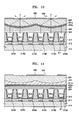
- the PDP comprises a lower substrate 210 and an upper substrate 220 that are separated by a predetermined distance.
- a discharge space is formed between the lower substrate 210 and the upper substrate 220.
- a plurality of address electrodes 211 and a first dielectric layer 212 are formed, preferably in this sequence.
- a plurality of barrier ribs 213 are formed parallel to the address electrodes 211 and are spaced apart by a predetermined amount.
- the ribs 213 are formed on the first dielectric layer 212.
- the barrier ribs 213 partition the discharge space between the lower substrate 210 and the upper substrate 220, thereby defining discharge cells 214.
- a fluorescent layer 215 is formed on the upper surface of the first dielectric layer 212, and the side surfaces of the barrier ribs 213, thus forming inner walls of the discharge cells 214.
- the discharge cells 214 are preferably filled with a discharge gas.
- a plurality of cylindrical lenses 220a, 220b and 220c are formed on the lower surface of the upper substrate 220.
- the cylindrical lenses 220a, 220b and 220c correspond to each of the discharge cells 214, and are formed perpendicular to the address electrodes 211. It is preferable that the cylindrical lenses 220a, 220b and 220c are formed integrally with the upper substrate 220. This is achieved in processing the lower surface of the upper substrate 220 in a suitable manner.
- the cylindrical lenses 220a, 220b and 220c focus the visible lights generated in the discharge cells 214. The focussed light is emitted from the PDP.
- the present embodiment shows three cylindrical lenses 220a, 220b and 220c corresponding to each of the discharge cells 214, the number of cylindrical lenses corresponding to each of the discharge cells 214 may be changed to two or four or more.
- first and second discharge electrodes 221a and 221b are formed in pairs, one pair for each discharge cell 214.
- the discharge electrodes sustain a discharge and are formed perpendicular to the address electrodes 211.
- first and second bus electrodes 222a and 222b are formed on the lower surface of the first and second discharge electrodes 221a and 221b. These are preferably made of metal.
- a second dielectric layer 223 is preferably formed on the lower surface of the cylindrical lenses 220a, 220b and 220c, so as to cover the first and second discharge electrodes 221a and 221b and the first and second bus electrodes 222a and 222b.
- a protective layer 224 is formed on the lower surface of the second dielectric layer 223.
- An external light shielding member is provided on the upper surface of the upper substrate 220 to prevent external light from entering the discharge cells 214 through the upper substrate 220.
- the external light shielding member is preferably formed of a plurality of parallel stripes 230 (preferably black) and are located on the upper surface of the upper substrate 220; each stripe 230 being spaced apart from one another by a predetermined amount.
- the stripes 230 are of constant width and are parallel with the cylindrical electrodes 220a, 220b and 220c.
- the stripes 230 are formed where no visible light is emitted by the discharge cells 214. Non-glare treatments are applied between the stripes 230.
- the stripes 230 may include a conductive film for shielding electromagnetic interference (EMI).
- EMI electromagnetic interference
- a transparent material layer 250 is formed to cover the lower surfaces of the cylindrical lenses 220a, 220b and 220c.
- First and second discharge electrodes 221a and 221b are preferably formed on the flat lower surface of the transparent material layer 250.
- First and second bus electrodes 222a and 222b are formed on the lower surfaces of the first and second discharge electrodes 221 a and 221b.
- a second dielectric layer 223 is formed on the lower surface of the transparent material layer 250 to cover the first and second discharge electrodes 221a and 221b and the first and second bus electrodes 222a and 222b.
- the transparent material layer 250 aids in forming the first and second discharge electrodes 221a and 221b and the first and second bus electrodes 222a and 222b.
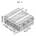
- the PDP comprises a lower substrate 310 and an upper substrate 320.
- the lower and upper substrates are spaced apart from each other by a predetermined distance.
- a discharge space is formed between the lower substrate 310 and the upper substrate 320.
- On the lower substrate 310 a plurality of address electrodes 311 and a first dielectric layer 312 are formed, preferably in this order.
- a plurality of barrier ribs 313 are formed on the first dielectric layer 312 in parallel to the address electrodes 311.
- the ribs 312 are spaced apart from one another by a predetermined distance.
- the barrier ribs 313 partition the discharge space between the lower substrate 310 and the upper substrate 320, thereby defining discharge cells 314.
- Red (R), green (G) and blue (B) fluorescent layers 315R, 315G and 315B are sequentially formed on the upper surface of the first dielectric layer 312, and side surfaces of the barrier ribs 313 forming the inner walls of the discharge cells 314.
- the discharge cells 314 are preferably filled with a discharge gas, which is a mixture of neon (Ne) and a small amount of xenon (Xe), as is generally used for plasma discharge.
- a plurality of cylindrical lenses 320a are formed on the lower surface of the upper substrate 320.
- Each of the cylindrical lenses 320a correspond to a plurality of the respective discharge cells 314.
- each of the cylindrical lenses 320a corresponds to one pixel of the PDP as shown in Figures 9 and 10.
- each of the cylindrical lenses 320a corresponds to three discharge cells 314 in which the red (R), green (G) and blue (B) fluorescent layers 315R, 315G and 315B are formed.
- the cylindrical lenses 320a are formed integrally with the upper substrate 320, which can be achieved during the processing of the lower surface of the upper substrate 320.
- the cylindrical lenses 320a focus the visible light generated in the three discharge cells 314 in which the red (R), green (G) and blue (B) fluorescent layers 315R, 315G and 315B are formed and emit the visible light out of the PDP.
- the cylindrical lenses 320a on the lower surface of the upper substrate 320 each correspond to one pixel.
- the lenses reduce the loss of visible light generated by discharge which enhances the brightness of the PDP.
- each of the cylindrical lenses 320a is shared by three discharge cells 314, the processing of the cylindrical lenses 320a is simpler and the PDP can be less expensive to manufacture.
- first and second discharge electrodes 321a and 321b for sustaining discharge are formed, in pairs, for each discharge cell 314.
- the first and second discharge electrodes 321a and 321b are formed perpendicular to the address electrodes 311.
- first and second bus electrodes 322a and 322b are formed on the lower surface of the first and second discharge electrodes 321 a and 321 b. These are preferably made of metal.
- a second dielectric layer 323 is formed on the lower surface of the cylindrical lenses 320a to cover the first and second discharge electrodes 321a and 321b and the first and second bus electrodes 322a and 322b.
- a protective layer 324 is formed on the lower surface of the second dielectric layer 323.
- the external light shielding member is provided on the upper surface of the upper substrate 320 to prevent external light from entering the discharge cells 314 through the upper substrate 320.
- the external light shielding member is preferably formed of a plurality of parallel stripes 330 (preferably black) on the upper surface of the upper substrate 320. These are spaced apart by a predetermined amount.
- the stripes 330 are preferably of a uniform width and are parallel with the address electrodes 311 and the cylindrical electrodes 320a.
- the stripes 330 are formed in a location where no visible light is emitted by the discharge cells 314. Non-glare treatments are applied to portions between the black stripes 330.
- the stripes 330 prevent external light from entering the discharge cells 314, thereby enhancing the bright room contrast of the PDP.
- the stripes 330 may include a conductive film for shielding electro magnetic interference (EMI).
- EMI electro magnetic interference
- a transparent material layer 350 is formed to cover the lower surfaces of the cylindrical lenses 320a.
- First and second discharge electrodes 321a and 321b are formed on the flat lower surface of the transparent material layer 350.
- First and second bus electrodes 322a and 322b are formed on the lower surfaces of the first and second discharge electrodes 321a and 321b.
- a second dielectric layer 323 is formed on the lower surface of the transparent material layer 350, to cover the first and second discharge electrodes 321a and 321 b and the first and second bus electrodes 322a and 322b.
- the transparent material layer 350 aids in forming the first and second discharge electrodes 321a and 321b and the first and second bus electrodes 322a and 322b.
- the PDP made according to embodiments of the present invention has the following features:
- black stripes can cover more of the upper surface of the upper substrate than in the known PDP, to more effectively prevent external light from entering the discharge cells, and thus, enhance the bright room contrast of the PDP.
- one cylindrical lens corresponds to two or more discharge cells, making the formation of the cylindrical lenses 320a simpler, so that the PDP can be less expensive to manufacture.
Landscapes
- Physics & Mathematics (AREA)
- Engineering & Computer Science (AREA)
- Plasma & Fusion (AREA)
- Electromagnetism (AREA)
- Signal Processing (AREA)
- Gas-Filled Discharge Tubes (AREA)
- Devices For Indicating Variable Information By Combining Individual Elements (AREA)
Applications Claiming Priority (2)
| Application Number | Priority Date | Filing Date | Title |
|---|---|---|---|
| KR1020040024510A KR20050099261A (ko) | 2004-04-09 | 2004-04-09 | 플라즈마 디스플레이 패널 |
| KR2004024510 | 2004-04-09 |
Publications (2)
| Publication Number | Publication Date |
|---|---|
| EP1585161A2 true EP1585161A2 (de) | 2005-10-12 |
| EP1585161A3 EP1585161A3 (de) | 2009-04-01 |
Family
ID=34910102
Family Applications (1)
| Application Number | Title | Priority Date | Filing Date |
|---|---|---|---|
| EP05102835A Withdrawn EP1585161A3 (de) | 2004-04-09 | 2005-04-11 | Plasmaanzeigetafel |
Country Status (5)
| Country | Link |
|---|---|
| US (1) | US7166962B2 (de) |
| EP (1) | EP1585161A3 (de) |
| JP (1) | JP2005302716A (de) |
| KR (1) | KR20050099261A (de) |
| CN (1) | CN100378896C (de) |
Cited By (1)
| Publication number | Priority date | Publication date | Assignee | Title |
|---|---|---|---|---|
| EP1840601A1 (de) * | 2006-03-28 | 2007-10-03 | Samsung SDI Co., Ltd. | Filteranordnung für eine Anzeigetafel und Anzeigevorrichtung damit |
Families Citing this family (7)
| Publication number | Priority date | Publication date | Assignee | Title |
|---|---|---|---|---|
| KR20050099260A (ko) * | 2004-04-09 | 2005-10-13 | 삼성전자주식회사 | 플라즈마 디스플레이 패널 |
| KR100665026B1 (ko) * | 2004-05-17 | 2007-01-09 | 삼성코닝 주식회사 | 디스플레이 필터, 이를 포함한 디스플레이 장치 및디스플레이 필터의 제조 방법 |
| KR100684808B1 (ko) * | 2006-02-16 | 2007-02-22 | 삼성에스디아이 주식회사 | 플라즈마 디스플레이 패널 |
| KR20070084859A (ko) * | 2006-02-22 | 2007-08-27 | 엘지전자 주식회사 | 플라즈마 디스플레이 패널 |
| KR20080057760A (ko) * | 2006-12-20 | 2008-06-25 | 엘지전자 주식회사 | 플라즈마 디스플레이 패널 |
| KR100829504B1 (ko) * | 2007-07-24 | 2008-05-16 | 엘지전자 주식회사 | 플라즈마 디스플레이 장치 |
| KR20090015748A (ko) * | 2007-08-09 | 2009-02-12 | 삼성모바일디스플레이주식회사 | 백라이트 유닛 및 이를 채용한 화상 표시 장치 |
Family Cites Families (26)
| Publication number | Priority date | Publication date | Assignee | Title |
|---|---|---|---|---|
| JPH0638363Y2 (ja) | 1987-08-27 | 1994-10-05 | 岡谷電機産業株式会社 | カラ−プラズマデイスプレイパネル |
| JP3033180B2 (ja) * | 1990-10-30 | 2000-04-17 | 富士通株式会社 | 交流型ガス放電パネルの製造方法 |
| JP3136178B2 (ja) | 1991-10-09 | 2001-02-19 | 株式会社リコー | ディスプレイ装置 |
| JPH08138559A (ja) * | 1994-11-11 | 1996-05-31 | Hitachi Ltd | プラズマディスプレイ装置 |
| JPH08152594A (ja) | 1994-11-25 | 1996-06-11 | Casio Comput Co Ltd | 液晶プロジェクタ |
| CN1146941C (zh) * | 1995-08-25 | 2004-04-21 | 富士通株式会社 | 一种表面放电的等离子体显示面板及其制造方法 |
| JP3627944B2 (ja) | 1996-05-21 | 2005-03-09 | 大日本印刷株式会社 | ホログラムカラーフィルターを用いた液晶表示装置 |
| DE69739681D1 (de) * | 1996-09-26 | 2010-01-14 | Asahi Glass Co Ltd | Schutzplatte für ein Plasma-Display und Verfahren zur Herstellung derselben |
| JP3497687B2 (ja) | 1997-01-30 | 2004-02-16 | パイオニア株式会社 | プラズマディスプレイ装置及びマルチプラズマディスプレイ装置 |
| TW417025B (en) * | 1997-04-10 | 2001-01-01 | Sumitomo Chemical Co | Front plate for plasma display |
| KR19980077351A (ko) * | 1997-04-18 | 1998-11-16 | 손욱 | 플라즈마 디스플레이 장치 및 그것의 제조 방법 |
| KR19980085527A (ko) | 1997-05-29 | 1998-12-05 | 손욱 | 입체 영상 디스플레이용 패널 및 이 패널에 적합한 렌티큘라 렌즈의 제조방법 |
| KR100236457B1 (ko) | 1997-06-28 | 1999-12-15 | 김영환 | 플라즈마 디스플레이 패널의 색순도 개선구조 |
| KR19990043630A (ko) | 1997-11-29 | 1999-06-15 | 김영남 | 플라즈마 표시소자 및 그 제조방법 |
| JP3464155B2 (ja) * | 1998-09-30 | 2003-11-05 | 三菱電機株式会社 | ディスプレイ装置及びその製造方法 |
| WO2000039830A1 (en) * | 1998-12-24 | 2000-07-06 | Koninklijke Philips Electronics N.V. | Image display panel |
| JP2001154597A (ja) | 1999-11-25 | 2001-06-08 | Toppan Printing Co Ltd | プラズマディスプレイパネル前面板 |
| JP2002182008A (ja) * | 2000-10-04 | 2002-06-26 | Sharp Corp | 光学レンズシステム、画像表示装置、マイクロレンズアレイ、液晶表示素子および投影型液晶表示装置 |
| JP2002350823A (ja) * | 2001-05-28 | 2002-12-04 | Sony Corp | 液晶表示素子および投射型液晶表示装置 |
| KR100440955B1 (ko) | 2001-09-11 | 2004-07-21 | 삼성전자주식회사 | 2d/3d 겸용 디스플레이 |
| EP1339082A1 (de) * | 2002-02-25 | 2003-08-27 | Asahi Glass Company Ltd. | Schlagfester Film für eine flache Anzeigetafel, und flache Anzeigetafel |
| KR20040018713A (ko) * | 2002-08-26 | 2004-03-04 | 삼성전자주식회사 | 기능성 소재를 포함한 디스플레이 장치의 스크린 및 그제조방법 |
| US7420322B2 (en) * | 2003-06-27 | 2008-09-02 | Casio Computer Co., Ltd. | Display device including a flat panel display panel |
| KR100522613B1 (ko) * | 2003-10-22 | 2005-10-19 | 삼성전자주식회사 | 플라즈마 디스플레이 패널 |
| KR20050099260A (ko) * | 2004-04-09 | 2005-10-13 | 삼성전자주식회사 | 플라즈마 디스플레이 패널 |
| KR100665026B1 (ko) * | 2004-05-17 | 2007-01-09 | 삼성코닝 주식회사 | 디스플레이 필터, 이를 포함한 디스플레이 장치 및디스플레이 필터의 제조 방법 |
-
2004
- 2004-04-09 KR KR1020040024510A patent/KR20050099261A/ko not_active Withdrawn
-
2005
- 2005-03-03 US US11/070,376 patent/US7166962B2/en not_active Expired - Fee Related
- 2005-04-01 JP JP2005106432A patent/JP2005302716A/ja active Pending
- 2005-04-08 CN CNB2005100638263A patent/CN100378896C/zh not_active Expired - Fee Related
- 2005-04-11 EP EP05102835A patent/EP1585161A3/de not_active Withdrawn
Cited By (1)
| Publication number | Priority date | Publication date | Assignee | Title |
|---|---|---|---|---|
| EP1840601A1 (de) * | 2006-03-28 | 2007-10-03 | Samsung SDI Co., Ltd. | Filteranordnung für eine Anzeigetafel und Anzeigevorrichtung damit |
Also Published As
| Publication number | Publication date |
|---|---|
| US20050225240A1 (en) | 2005-10-13 |
| CN100378896C (zh) | 2008-04-02 |
| JP2005302716A (ja) | 2005-10-27 |
| EP1585161A3 (de) | 2009-04-01 |
| CN1681066A (zh) | 2005-10-12 |
| KR20050099261A (ko) | 2005-10-13 |
| US7166962B2 (en) | 2007-01-23 |
Similar Documents
| Publication | Publication Date | Title |
|---|---|---|
| US7088043B2 (en) | Plasma display panel enhancing a bright room contrast | |
| KR100842979B1 (ko) | 플라즈마 디스플레이 장치 | |
| EP1585161A2 (de) | Plasmaanzeigetafel | |
| KR20050045513A (ko) | 플라즈마 디스플레이 패널 | |
| EP1745498B1 (de) | Plasmaanzeigetafel | |
| US8058804B2 (en) | Display device having light blocking members | |
| KR100522613B1 (ko) | 플라즈마 디스플레이 패널 | |
| US7372203B2 (en) | Plasma display panel having enhanced luminous efficiency | |
| KR20050036448A (ko) | 플라즈마 디스플레이 패널 | |
| US7728522B2 (en) | Plasma display panel | |
| KR100368763B1 (ko) | 주 격벽과 보조 격벽 구조를 갖는 교류형 플라즈마 디스플레이 장치 | |
| KR100560543B1 (ko) | 플라즈마 디스플레이 패널 | |
| KR100502921B1 (ko) | 플라즈마 디스플레이 패널 | |
| US6590339B2 (en) | Plasma display panel | |
| CN100573793C (zh) | 等离子体显示面板 | |
| KR20060101918A (ko) | 플라즈마 디스플레이 패널 | |
| KR20050097252A (ko) | 플라즈마 디스플레이 패널 | |
| KR20020079201A (ko) | 플라즈마 표시장치 | |
| KR20060037734A (ko) | 플라즈마 디스플레이 패널 및 이를 구비한 평판 표시 장치 | |
| KR20050112822A (ko) | 플라즈마 디스플레이 패널 |
Legal Events
| Date | Code | Title | Description |
|---|---|---|---|
| PUAI | Public reference made under article 153(3) epc to a published international application that has entered the european phase |
Free format text: ORIGINAL CODE: 0009012 |
|
| AK | Designated contracting states |
Kind code of ref document: A2 Designated state(s): AT BE BG CH CY CZ DE DK EE ES FI FR GB GR HU IE IS IT LI LT LU MC NL PL PT RO SE SI SK TR |
|
| AX | Request for extension of the european patent |
Extension state: AL BA HR LV MK YU |
|
| PUAL | Search report despatched |
Free format text: ORIGINAL CODE: 0009013 |
|
| AK | Designated contracting states |
Kind code of ref document: A3 Designated state(s): AT BE BG CH CY CZ DE DK EE ES FI FR GB GR HU IE IS IT LI LT LU MC NL PL PT RO SE SI SK TR |
|
| AX | Request for extension of the european patent |
Extension state: AL BA HR LV MK YU |
|
| AKX | Designation fees paid | ||
| REG | Reference to a national code |
Ref country code: DE Ref legal event code: 8566 |
|
| STAA | Information on the status of an ep patent application or granted ep patent |
Free format text: STATUS: THE APPLICATION IS DEEMED TO BE WITHDRAWN |
|
| 18D | Application deemed to be withdrawn |
Effective date: 20091002 |