EP1583259B1 - Lichtquellenvorrichtung und Verfahren zur redundanten Schaltung dieser Lichtquelle - Google Patents
Lichtquellenvorrichtung und Verfahren zur redundanten Schaltung dieser Lichtquelle Download PDFInfo
- Publication number
- EP1583259B1 EP1583259B1 EP04016462A EP04016462A EP1583259B1 EP 1583259 B1 EP1583259 B1 EP 1583259B1 EP 04016462 A EP04016462 A EP 04016462A EP 04016462 A EP04016462 A EP 04016462A EP 1583259 B1 EP1583259 B1 EP 1583259B1
- Authority
- EP
- European Patent Office
- Prior art keywords
- optical pulse
- optical
- pulse train
- section
- output
- Prior art date
- Legal status (The legal status is an assumption and is not a legal conclusion. Google has not performed a legal analysis and makes no representation as to the accuracy of the status listed.)
- Expired - Lifetime
Links
Images






Classifications
-
- H—ELECTRICITY
- H04—ELECTRIC COMMUNICATION TECHNIQUE
- H04J—MULTIPLEX COMMUNICATION
- H04J14/00—Optical multiplex systems
- H04J14/02—Wavelength-division multiplex systems
- H04J14/0287—Protection in WDM systems
- H04J14/0297—Optical equipment protection
-
- H—ELECTRICITY
- H04—ELECTRIC COMMUNICATION TECHNIQUE
- H04B—TRANSMISSION
- H04B10/00—Transmission systems employing electromagnetic waves other than radio-waves, e.g. infrared, visible or ultraviolet light, or employing corpuscular radiation, e.g. quantum communication
- H04B10/03—Arrangements for fault recovery
- H04B10/032—Arrangements for fault recovery using working and protection systems
-
- H—ELECTRICITY
- H04—ELECTRIC COMMUNICATION TECHNIQUE
- H04B—TRANSMISSION
- H04B10/00—Transmission systems employing electromagnetic waves other than radio-waves, e.g. infrared, visible or ultraviolet light, or employing corpuscular radiation, e.g. quantum communication
- H04B10/50—Transmitters
- H04B10/508—Pulse generation, e.g. generation of solitons
Definitions
- the present invention relates to a light source apparatus suitable for use in an optical communications system, as well as to a method for switching redundancy of the light source.
- US-B1-6,324,318 discloses a technique of producing a substitute light of a wavelength identical to that of a faulty working light source which is one of a plurality of working light sources having different wavelengths by optical four wave mixing, and replacing the transmission light of the faulty working light source by the substitute light.
- US 2003/012 495 A1 discloses a method and system for generating a broadband spectral continuum using short spans of constant dispersion, dispersion-shifted fibers.
- US 2001/046 344 A1 discloses an optical signal switching apparatus whose hardware can be commonly used for the 1+1 switching structure and the 1:1 switching structure by combining optical signals using a variable optical coupler.
- WDM Wavelength Division Multiplexing
- Asemiconductorlaser which emits a Continuous Wave (CW) of single wavelength has hitherto been widely employed as a signal source in a WDM system.
- CW Continuous Wave
- a current light source and a backup light source In order to implement a redundancy configuration for the case of occurrence of a failure in the light sources, a current light source and a backup light source must be provided for each working wavelength.
- constructing a WDM communications system through use of a light source which generates a single wavelength requires light sources which are equal in number to the operational channels.
- temperature control and monitoring of a wavelength must be performed on a per-device basis.
- the redundancy configuration is implemented in the light source through use of the plurality of light sources provided in equal number to the operational channels, in the event that trouble has arisen in CW light (continuous light) generated from the respective light sources, a state in which no light is generated (a cutoff state) arises between a time when the trouble has been detected and a time when the switch is changed.
- a period of time during which the CW light is cut off is responsible for occurrence of a problem in communication, such as a transmission error.
- the super continuum light source which is a technique for collectively generating an optical carrier ranging from hundreds of wavelengths to thousands of wavelengths.
- the SC light source involves simple temperature control. Further, with an increase in the number of channels, a footprint of the light sources and power consumed by the light sources do not become tremendous.
- Patent Document 1 relates to an optical circuit which enables an improvement in product yield. Specifically, Patent Document 1 describes a multi-wavelength light source optical circuit into which are integrated a plurality of DFB lasers corresponding to optical elements.
- Patent Document 1 is intended for embodying a redundancy configuration for the case where the DFB lasers differ from each other in terms of an oscillation wavelength. Hence, the technique is not applicable to implementation of the redundancy configuration using the SC light sources, such as that mentioned previously.
- a light source apparatus comprising: a plurality of optical pulse train generation sections capable of generating a plurality of periodic optical pulse trains which are in synchronism with each other and have substantially the same repetition cycle; an optical switch section capable of selectively outputting an optical pulse train to be taken as an optical pulse train for current use from among saidplurality of optical pulse trains output from said plurality of optical pulse train generation sections; an output light generation section capable of generating continuous light having an enlarged wavelength spectrum from said optical pulse train output from said optical switch section; and an optical switch control section for controlling said optical switch section in such a manner that said optical switch section switches an output of said optical pulse train for current use from said optical switch section at the extinction timing of said plurality of optical pulse trains, in accordance with the states of respective optical pulse trains generated by said plurality of optical pulse train generation sections.
- a method for switching redundancy of a light source employing an output light generation section capable of generating continuous light having an enlarged wavelength spectrum as output light from a periodic optical pulse train comprising: using a plurality of optical pulse train generation sections capable of generating a plurality of periodic optical pulse trains which are in synchronism with each other and have substantially the same repetition cycle; selecting any one of said plurality of optical pulse train generation sections for current use and causing said output light generation section to generate said output light from said periodic optical pulse train output from the selected optical pulse train generation section for current use; and switching, among said plurality of optical pulse train generation sections, any of the optical pulse train generation sections not employed for current use to current use, where the time of switching of said optical pulse train generation section for current use occurs at an extinction timing of said plurality of optical pulse trains, and causing said output light generation section to generate said output light from the periodic optical pulse train output from said optical pulse train generation section switched for current use.
- the following describes a light source apparatus which enables switching from a current system to a backup system using an SC light source without involvement of instantaneous interruption of power, to thus avoid, e.g., interruption of CW light in the course of being output when switching is made to the backup system upon detection of a failure, as well as providing a method for switching redundancy of the light source apparatus.
- the light source apparatus is characterized by including a plurality of optical pulse train generation sections capable of generating periodic optical pulse trains in synchronism with each other; an optical switch section capable of selectively outputting an optical pulse train to be taken as an optical pulse train for current use from among the optical pulse trains output from the plurality of optical pulse train generation sections; an output light generation section capable of generating continuous light having a plurality of wavelengths from the optical pulse train output from the optical switch section; and an optical switch control section for controlling the optical switch section in order to switch an output of the optical pulse train for current use from the optical switch section, in accordance with the states of respective optical pulse trains generated by the plurality of optical pulse train generation sections and without involvement of instantaneous power interruption.
- the optical switch control section preferably further includes photoelectric conversion sections for converting into electrical signals the respective optical pulse trains output from the plurality of optical pulse train generation sections; an anomaly detection section for detecting anomalies in the respective optical pulse trains converted into electrical signals by the photoelectric conversion sections; a timing extraction section for extracting extinction/illumination timings of the respective optical pulse trains converted into the electrical signals by the photoelectric conversion sections; and the first control signal output section which, when the anomaly detection section has detected anomalies in the optical pulse train for current use, outputs the first control signal to the optical switch section in order to switch the optical pulse train for current use, at an extinction timing extracted by the timing extraction section.
- each of the plurality of optical pulse train generation sections may include a clock signal generation section for generating a clock signal, and a pulse light source for outputting optical pulse trains on the basis of the clock signal generated by the clock signal generation section.
- the light source apparatus may further include a sync control section for synchronously controlling the clock signal generation sections of the respective optical pulse train generation sections on the basis of extinction/illumination timings of the respective optical pulse trains extracted by the timing extraction section.
- the light source apparatus may also further include node sections, each of which divides the respective optical pulse train output from the plurality of optical pulse train generation sections into two branches and which guides one of the branches to the optical switch section and the other branch to the respective photoelectric conversion section, and a light delay circuit can also be interposed between the node section and the optical switch section, the light delay circuit delaying propagation of the respective optical pulse trains.
- the light source apparatus can also further include the node sections, each of which divides the respective optical pulse trains output from the plurality of optical pulse train generation sections into two branches and which guides one of the branches to the optical switch section and the other branch to the photoelectric conversion sections; light delay circuits each being interposed between the corresponding node section and the optical switch section and which delays propagation of the respective optical pulse train; and chirp compensation circuits, each of which is interposed between the respective node section and the optical switch section and which compensates for chirp.
- the optical switch section may further include first and second optical switches which are under control of the optical switch control section, receive optical pulse trains output from the plurality of optical pulse train generation sections, and can selectively output an optical pulse train for current use among the received optical pulse trains; and a switch-to-be-used changeover control section for controlling switching between the first optical switch and the second optical switch such that the first optical switch is used in normal times for selectively outputting the optical pulse train for current use and the second optical switch is used for selectively outputting another optical pulse train for current use in the event of occurrence of anomalies in the optical pulse train for current use output from the first optical switch.
- the first and second optical switches each include a current optical pulse train output port for outputting the optical pulse train for current use among the plurality of optical pulse trains output from the optical pules train generation sections, and a backup optical pulse train output port for outputting a backup output pulse train other than the current optical pulse train, for monitoring purpose.
- the switch-to-be-used changeover control section may be configured to determine occurrence of anomalies in any one of the first and second optical switches, by means of monitoring the backup output pulse train output from the backup optical pulse train output ports of the respective first and second optical switches.
- a light delay circuit may also be interposed between the first optical switch and the output light generation section for delaying propagation of an optical pulse train output from the first optical switch.
- a light delay circuit for delaying propagation of an optical pulse train output from the first optical switch and a chirp compensation circuit for effecting chirp compensation may be interposed between the first optical switch and the output light generation section.
- the light source apparatus may also further include a light phase adjustment section for compensating a difference between a time when respective optical pulse trains output from the plurality of optical pulse trains arrive at the first optical switch and a time when respective optical pulse trains output from the plurality of optical pulse trains arrive at the second optical switch.
- the optical switch control section may include a status determination section for determining the status of an optical pulse train output for current use from the optical switch section, on the basis of variations in a specific wavelength component in continuous light of multiple wavelengths generated as the output light by the output light generation section; and the second control signal output section for outputting the second control signal to the optical switch section in order to switch an output of the optical pulse train for current use from the optical switch section without involvement of instantaneous power interruption when the status determination section determines the status of the optical pulse train output for current use from the optical switch section to be anomalous.
- the following also describes a method for switching redundancy of a light source apparatus corresponding to a method for switching redundancy of a light source employing an output light generation section capable of generating continuous light of multiple wavelengths as output light from a periodic optical pulse train, the method including: using a plurality of optical pulse train generation sections capable of generating the optical pulse train; employing any one of the plurality of optical pulse train generation sections for current use and causing the output light generation section to generate the output light from the periodic optical pulse train output from the optical pulse train generation section for current use; and switching, among the plurality of optical pulse train generation sections, any of optical pulse train generation sections not having been employed for current use to an optical pulse train for current use without involvement of instantaneous power interruption at the time of switching of the optical pulse train generation section for current use, and causing the output light generation section to generate the output light from a periodic optical pulse train output from the optical pulse train generation section switched for current use.
- any of optical pulse train generation sections not having been employed for current use among the plurality of optical pulse train generation sections is preferably switched to an optical pulse train for current use at an extinction timing of the optical pulse train, without involvement of instantaneous power interruption.
- the optical switch control section is arranged to be able to switch the current system to the backup system through use of the SC light source without involvement of instantaneous interruption of power. Even in the event that, for instance, a failure has arisen in the optical pulse train generation section of the current system, the optical pulse train can be switched to another optical pulse train output from the optical pulse generation section of the backup system without involvement of instantaneous interruption of power, thereby yielding an advantage of the ability to stably generate and output continuous light which is to become output light.
- the first optical switch can be changed to the second optical switch without instantaneous interruption of power, by means of the switch-to-be-used changeover control section along with the first and second optical switches.
- CW light continuous light
- the switch-to-be-used changeover control section along with the first and second optical switches.
- FIG. 1 is a block diagram showing a light source apparatus according to the first embodiment of the present invention.
- a light source apparatus 10 shown in Fig. 1 comprises optical pulse train generation sections 1-1, 1-2; tap couplers 2-1, 2-2; an optical switch 3; an optical switch control section 6; and a high nonlinear fiber 7.
- the light source apparatus 10 acts as an SC light source and also switches the current system to a backup system without instantaneous interruption of power in the event of occurrence of a failure, thereby preventing CW light which is now output from entering a disconnected state.
- the light source train generation sections 1-1, 1-2 can respectively generate periodic pulse trains in synchronism with each other.
- the optical pulse train generation section 1-1 comprises a pulse drive circuit 1a and a short pulse light source 1b-1, and the optical pulse train generation section 1-2 shares the pulse drive circuit 1a and comprises another short pulse light source 1b-2.
- the pulse drive circuit 1a acts as a clock signal generation section for generating a clock signal (having a frequency of, e.g., 10 GHz or thereabouts) to be used for producing an optical pulse train.
- the optical pulse train generation sections 1-1, 1-2 use the single pulse drive circuit 1a in a shared manner, thereby generating synchronized optical pulse trains. Even when using separate pulse drive circuits, the pulse train generation sections 1-1, 1-2 can generate synchronized optical pulse trains, so long as they are provided with a circuit for bringing the separate pulse drive circuits in synchronism with each other as shown in, e.g., Fig. 9 which will be described later.
- the short pulse light sources (pulse light sources) 1b-1, 1b-2 output optical pulse trains on the basis of a clock signal produced by the pulse drive circuit 1a.
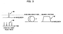
- the optical pulse trains generated by the short pulse light sources 1b-1, 1b-2 each have, e.g., a wavelength spectrum required to generate a short pulse, as indicated by a waveform WA shown in Fig. 3 , and correspond to an optical pulse train (e.g., a short pulse train having a repetition cycle of about a few picoseconds to hundreds of femtoseconds) in synchronism with the pulse signal output from the pulse drive circuit 1a (see a waveform WB shown in Fig. 3 ).
- the tap couplers (node sections) 2-1, 2-2 each bifurcate, into two sub-pulse trains, the respective optical pulse trains output from the optical pulse train generation sections 1-1, 1-2 and guide one of the two sub-pulse trains to the optical switch 3 and the remaining sub-pulse train to the optical switch control section 6.
- the optical switch 3 functions as an optical switch section for selectively outputting either of the optical pulse trains output from the optical pulse train generation sections 1-1, 1-2.
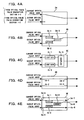
- the optical switch 3 can be embodied as, e.g., a 2x1 single-stage optical switch 3A shown in Fig. 4A , a two-stage tandem switch 3B shown in Fig. 4B , an optical switch 3C shown in Fig. 4C , an optical switch 3D additionally provided with a monitor port shown in Fig. 4D , or an optical switch 3E additionally provided with a monitor port shown in Fig. 4E . Even when any one of the optical switches 3A to 3E has been employed, the optical switch can select an optical pulse train under switching control of the optical switch control section 6 to be described later.
- the single-stage optical switch 3A shown in Fig. 4A can be formed from a semiconductor, an optical switch of directional coupler type using a dielectric waveguide, or an optical switch of Mach- Zehnder interferometer type.
- the single stage optical switch 3A may be formed by utilization of another known device.
- the optical pulse trains output from the optical pulse train generation sections 1-1, 1-2 are input to two input ports, respectively.
- an electrical signal serving as a changeover control signal output from the optical switch control section 6 is applied to the single-stage optical switch 3A, thereby enabling the single stage optical switch 3A to output an optical pulse train through switching operation.
- two optical switch elements 3b-1, 3b-2 are provided in parallel on the input side of the optical switch, and an optical switch 3b- 3 is provided on the output side of the optical switch elements 3b-1, 3b-2, whereby the optical switch elements 3b-1 to 3b-3 are arranged in a two-stage tandem connection.
- the optical switch elements 3b-1 to 3b-3 can be formed from a semiconductor, an optical switch of directional coupler type using a dielectric waveguide, or an optical switch of Mach-Zehnder interferometer type.
- the optical switch elements 3b-1 to 3b-3 may be formed by utilization of another known device.
- optical pulse trains output from the respective optical pulse generation sections 1-1, 1-2 are input to respective input ports of the optical switch elements 3b-1, 3b-2.
- the electrical signal serving as a changeover control signal is applied by the switch control section 6 to the optical switch elements 3b-1 to 3b-3.
- a selected optical pulse train can be output from the output port of the optical switch element 3b-3.
- the optical switch 3C shown in Fig. 4C comprises light gates 3c-1, 3c-2 for switching between interruption of an input optical pulse train and leading of an input optical pulse train in accordance with the electrical signal which is output from the switch control section 6 and acts as a changeover control section; and a 3dB coupler 3c-3.
- the optical pulse trains output from the optical pulse train generating sections 1-1, 1-2 are input to the light gates 3c-1, 3c-2, respectively.
- the electrical signal serving as a changeover control signal is applied by the switch control section 6 to the light gates 3c-1, 3c-2, whereby the optical coupler 3c-3 can output the selected optical pulse train.
- An light gate of Mach-Zehnder interferometer type, an light gate utilizing absorbing and amplifying characteristics of a semiconductor optical amplifier, and a light gate using an absorbing characteristic of an EA (Electro-Absorption) modulator (semiconductor modulator of absorption type) are mentioned as the light gates 3c-1, 3c-2.
- the light gates 3c-1, 3c-2 may also be formed by utilization of another known device.
- the optical switch 3D shown in Fig. 4D is formed from a semiconductor, an optical switch of directional coupler type using a dielectric waveguide, or an optical switch of Mach-Zehnder interferometer type.
- the optical pulse trains output from the optical pulse train generation sections 1-1, 1-2 are input by way of two input ports 3d-1, 3d-2.
- the optical pulse train output from the optical pulse train generation section 1-1 can be output, by way of an output port 3d-3, as the optical pulse train selected by the changeover control signal.
- the optical pulse train output from the optical pulse train generation section 1-2 can be output as a backup optical pulse train by way of an output port 3d-4.
- the two-stage tandem optical switch 3E shown in Fig. 4E comprises a two-stage tandem configuration consisting of three optical switch elements 3e-1 to 3e-3.
- the optical pulse trains output from the optical pulse train generation sections 1-1, 1-2 are input to the input ports 3e-1 to 3e-3 by way of two input ports 3e-4, 3e-5.
- An optical pulse train selected by the changeover control signal can be output by way of an output port 3e-6.
- optical pulse train output from the optical pulse train generation section 1-1 can be output as an unselected backup optical pulse train by way of an output port 3e-7
- optical pulse train output from the optical pulse train generation section 1-2 can be output as an unselected backup optical pulse train by way of an output port 3e-8.
- the high nonlinear fiber 7 functions as an output light generation section capable of generating continuous light of a plurality of wavelengths, as output light, from the optical pulse train output from the optical switch 3.
- either of the optical pulse trains generated by the optical pulse train generation sections 1-1, 1-2 e.g. , the optical pulse train generated by the optical pulse train generation section 1-1) is caused to enter the high nonlinear fiber 7 by way of the optical switch 3 while satisfying an optical power level and conditions for a phase between optical carrier side lobes to be used for generating pulses. Consequently, a plurality of optical carriers can be generated at a wavelength (frequency) interval corresponding to the repetition frequency of the thus-input optical pulse train.
- An enlarged spectrum waveform WC shown in Fig. 3 represents a wavelength spectrum of continuous light which is an output from the high nonlinear fiber 7. As indicated by the englarged by the spectrum waveform WC shown in Fig. 3 , a plurality of optical carriers can be generated at the wavelength (frequency) interval corresponding to the repetition frequency while light of single wavelength is taken as input light.
- the optical switch control section 6 is for controlling the optical switch 3 so as to switch the output of optical pulse train, which is taken as a current optical pulse train by the optical switch 3, in accordance with the states of the respective optical pulse trains generated by the optical pulse train generation sections 1-1, 1-2 without involvement of instantaneous interruption of power.
- the optical switch control section 6 is formed from photodiodes 4-1, 4-2 serving as photoelectric conversion sections, and an electrical signal processing section 5.
- the photodiode 4-1 converts the optical pulse train output from the optical pulse train generation section 1-1 into an electrical signal
- the photodiode 4-2 converts the optical pulse train output from the optical pulse train generation section 1-2 into an electrical signal.
- the electrical signal processing section 5 controls the optical switch 3 for the purpose of switching either of the optical pulse trains output from the optical pulse train generation sections 1-1, 1-2 to an optical pulse train for current use.
- the electrical signal processing section 5 comprises an anomaly detection section 5a, a timing extraction section 5b, and the first control signal output section 5c.
- the anomaly detection section 5a is for detecting anomalies in the respective optical pulse trains converted into the electrical signals by the photodiodes 4-1, 4-2. Specifically, the anomaly detection section 5a is arranged to sense a decrease in or loss of the optical power level of the optical pulse train used as a current pulse train, thereby detecting the decrease or loss as occurrence of a failure (an anomaly). In addition, the anomaly detection section 5a may detect occurrence of an anomaly by determining whether or not the pulse width, or the like, has fallen outside a prescribed range.
- the timing extraction section 5b is for extracting extinction/illumination timings of the respective optical pulse trains converted into the electrical signals by the photodiodes 4-1, 4-2. Specifically, the timing extraction section 5b extracts clock signal components, as illumination timings, from the respective optical pulse trains which have been converted into electrical signals by the photodiodes 4-1, 4-2 and are output from the optical pulse train generation sections 1-1, 1-2. An intermediate timing of the extracted clock signal components is extracted as an illumination timing.
- the first control signal output section 5c When the anomaly detection section 5a has detected anomalies in the optical pulse train taken as a pulse train for current use, the first control signal output section 5c outputs the first control signal to the optical switch 3 at the extinction timing extracted by the timing extraction section 5b, in order to switch the current optical pulse train (to the backup optical pulse train) without involvement of instantaneous interruption of power.
- the first control signal output section 5c is arranged to output a control signal (a changeover trigger) to the optical switch 3 so as to switch the backup optical pulse train generation section 1-2 to the current optical pulse train generation section.
- the optical pulse train generated by the optical pulse train generation section 1-2 can be output to the high nonlinear fiber 7 by way of the optical switch 3.
- the anomaly detection section 5a is required to have determined that no anomaly has arisen in the backup optical output pulse before the first control signal output section 5c outputs the control signal.
- the timing extraction section 5b extracts an extinction timing VT of optical pulse trains P1, P2 which are synchronously generated by and output from the optical pulse train generation sections 1-1, 1-2.
- the timing extraction section 5b then outputs the first control signal to the optical switch 3 such that the current optical pulse generation section 1-1 is switched to the backup optical pulse generation section 1-2 at the extinction timing VT.
- the optical pulse train output from the optical switch 3 is switched from the optical pulse train P1 to the optical pulse train P2 at the extinction timing VT.
- the extinction timing is a timing at which light levels of the two optical pulse trains P1, P2 output from the optical pulse train generation sections 1-1, 1-2 become zero.
- the optical switch 3 switches between the two optical pulse trains output from the optical pulse train generation sections 1-1, 1-2 at the timing of extinction, whereby after output the thus-output optical pulse train can be handled as if the pulse train originated from a single light source. Therefore, in the event that a failure has arisen in the current optical pulse generation section 1-1, the optical pulse train is output to the high nonlinear fiber 7 without disconnection (or while maintaining a repetition cycle); that is, without instantaneous interruption of power.
- either of the two optical pulse train generation sections 1-1, 1-2 (e.g., an optical pulse train generation section 1-1) is taken for current use, and the high nonlinear fiber 7 generates continuous light having a plurality of carriers, which is to become output light, from a periodic optical pulse train output from the current optical pulse train generation section 1-1 and outputs the thus-generated output light.
- the first control signal output section 5c outputs a changeover trigger, as the first control signal, to the optical switch 3 in order to switch the optical pulse train to be output to the high nonlinear fiber 7 between the two optical pulse trains output from the optical pulse train generation sections 1-1, 1-2.
- the first control signal output section 5c can output the first control signal such that the output pulse train is switched at the timing of extinction extracted by the timing extraction section 5b.
- the optical pulse train generation section 1-2 that has not been taken for current use is switched to the current optical pulse train generation section without involvement of instantaneous interruption of power.
- the high nonlinear fiber 7 stably generates continuous light ⁇ which is to come to output light and has a plurality of carriers ⁇ from the periodic optical pulse train output from the optical pulse train generation section 1-2 switched for current use and outputs the thus-generated continuous light (even when switching operation of the optical switch 3 has arisen).
- the current optical pulse train can be switched to the optical pulse train output from the backup optical pulse train generation section (e.g., the optical pulse train generation section 1-2) of the backup system without involvement of instantaneous interruption of power.
- the anomaly detection section 5a detects an anomaly upon detection of a decrease in the light level of the current optical pulse train, there is yielded an advantage of the ability to avoid interruption of the continuous light which is being output during a period from when a failure in the anomaly detection section 5a has been detected until when the current system is switched to the backup system.
- Fig. 6 is a block diagram showing a light source apparatus 10A of the first modification of the first embodiment of the invention.
- the light source apparatus 10A shown in Fig. 6 differs from the light source apparatus 10 of the first embodiment in that a light delay circuit 8A-1 for delaying propagation of an optical pulse train is interposed between the tap coupler 2-1 serving as a node section and the optical switch 3, as well as in that a light delay circuit 8A-2 for delaying propagation of the optical pulse train is interposed between the tap coupler 2-2 and the optical switch 3.
- the first modification is identical with the first embodiment.
- those reference numerals which are the same as those in Fig. 1 denote substantially identical sections.
- the light delay circuits 8A-1, 8A-2 can be formed from, e.g., an optical fiber.
- the present technique also allows adoption of a known device other than the optical fiber.
- a period of time from when the failure has actually arisen until when the optical switch 3 is switched is delayed by means of the light delay circuits 8A-1, 8A-2.
- the anomaly detection section 5a detects interruption of an optical signal, and the trigger signal output from the first control signal output section 5c can be sent to the optical switch 3 before arrival of the optical pulse train under the influence of the failure.
- detection of occurrence of a failure by the anomaly detection section 5a and switching operation of the optical switch 3 can be completed by means of the light delay circuits 8A-1, 8A-2 before the current optical pulse train responsible for detection of the failure arrives at the optical switch 3 by way of the node section 2-1.
- Fig. 7 is a view for describing operation of the light delay circuits 8A-1, 8A-2.
- optical pulse trains P11, P12 are assumed to be input to the light delay circuits 8A-1, 8A-2 .
- the optical pulse P11 is switched to the optical pulse train P12 output from the optical pulse train generation section 1-2 before a pulse PX responsible for detection of a failure at a point in time t1 arrives at the optical switch 3 through propagation delay by the light delay circuit 8A-1.
- the first control signal output section 5c outputs a changeover trigger to the optical switch 3 at the timing of extinction (e.g., points in time t2, t3 or t4; or the point in time t3 depicted on the right side in Fig. 7 ) in a stage where a normal optical pulse train preceding the pulse PX has been output.
- the optical pulse train is output from the optical switch 3 while maintaining a constant repetition cycle.
- Fig. 8 is a block diagram showing a light source apparatus 10B according to the second modification of the first embodiment according to the present invention.
- the light source apparatus 10B shown in Fig. 8 differs from the light source apparatus 10A in that light delay/chirp compensation circuits 8B-1, 8B-2 are provided in lieu of the light delay circuits 8A-1, 8A-2.
- the light source apparatus is identical in configuration with the light source apparatus shown in Fig. 6 .
- those reference numerals which are the same as those in Fig. 6 denote substantially identical sections.
- the light delay/chirp compensation circuit 8B-1 is interposed between the tap coupler 2-1 and the optical switch 3, and the light delay/chirp compensation circuit 8B-2 is interposed between the tap coupler 2-2 and the optical switch 3.
- Each of the light delay/chirp compensation circuits 8B-1, 8B-2 functions as a light delay circuit for delaying propagation of the respective optical pulse train and also functions to serve as a chirp compensation circuit for effecting chirp compensation.
- the light delay/chirp compensation circuits 8B-1, 8B-2 can be constituted of, e.g. , an optical fiber, or the like.
- the present technique also allows adoption of a known device other than the optical fiber for the light delay circuit and the chirp compensation circuit.
- the optical pulse trains output from the optical pulse train generation sections 1-1, 1-2 are subjected to a difference between the phase of a side lobe frequency and the center wavelength under influence of a frequency chirp due to modulation induced at the time of generation of a pulse.
- the optical pulse train with the phase difference is input to the high nonlinear fiber 7, the quality of continuous light (SC light) of a plurality of channels serving as output light is affected.
- the optical fibers which serve as the light delay/chirp compensation circuits 8B-1, 8B-2, have the same light delay function as that of the light delay circuits 8A-1, 8A-2 shown in Fig. 6 .
- the optical fibers In order to compensate for influence of the frequency chirp such as that mentioned above, the optical fibers have a wavelength dispersion characteristic for compensating for an initial chirp of the optical pulse trains output from the light pulse train generation sections 1-1, 1-2. More specifically, frequency chirp characteristics of the optical pulse trains generated by the optical pulse train generation sections 1-1, 1-2 have been measured in advance.
- the light delay/chirp compensation circuits 8B-1, 8B-2 are constituted of optical fibers having such a length as to compensate for a measured frequency chirp while ensuring a delay time for causing the optical fibers to act as light delay circuits.
- the anomaly detection section 5a can detect interruption of an optical signal, and the trigger signal output from the first control signal output section 5c can be sent to the optical switch 3 before the pulse under influence of the failure arrives at the optical switch 3.
- the pulse which would cause a failure, is prevented from entering the high nonlinear fiber 7, thereby switching the source for generating an optical pulse train to another source without instantaneous interruption of power.
- the optical pulse trains generated by the optical pulse train generation sections 1-1, 1-2 can be output to the optical switch 3 after the frequency chirps of the optical pulse trains have been compensated.
- the present embodiment can also yield an advantage of the ability to enhance the quality of the SC light output from the high nonlinear fiber 7, because the frequency chirps of the optical pulse trains generated by the optical pulse train generation sections 1-1, 1-2 can be compensated.
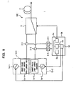
- Fig. 9 is a block diagram showing a light source apparatus 10C according to the thirdmodification of the first embodiment according to the present invention.
- the light source apparatus 10C shown in Fig. 9 differs from the light source apparatus of the first embodiment in that optical pulse train generation sections 1C-1, 1C-2 are provided with different pulse drive circuits 1a-1, 1a-2 and in that the light source apparatus is provided with a sync control section 5d for synchronizing clock signals output from the pulse drive circuits 1a-1 1a-2 of the respective optical pulse train generation sections 1C-1, 1C-2.
- An electrical signal processing section 5A of the light source apparatus 10C shown in Fig. 9 comprises an anomaly detection section 5a, a timing extraction section 5b, and the first control signal 5c, which are the same as those of the first embodiment.
- the electrical signal processing section 5A further comprises a sync control section 5d for controlling synchronization of the pulse drive circuits 1a-1, 1a-2 of the respective pulse train generation sections 1C-1, 1C-2 at the extinction/illumination timings of the respective optical pulse trains extracted by the timing extraction section 5b.
- the sync control section 5d On the basis of the clock signal components extracted from the optical pulse trains output from the optical pulse train generation sections 1C-1, 1C-2 by the timing extraction section 5b, the sync control section 5d detects jitter in the clock signal components and outputs a control signal to the respective pulse drive circuits 1a-1 1a-2 so as to suppress the detected jitter.
- the sync control section 5d imparts the sync control signal to, e.g., the pulse drive circuit 1a-2 of the backup optical pulse train generation section 1-2, thereby delaying the optical pulse train generated by the optical pulse train generation section 1-2.
- pulse timings of the optical pulse trains P15 , P16 generated by the respective optical pulse train generation sections 1C-1, 1C-2 can be made coincident with each other.
- the optical pulse train generation sections 1C-1, 1C-2 are provided with separate pulse drive circuits 1a-1, 1a-2, the optical pulse trains generated by the respective pulse train generation sections 1C-1, 1C-2 can be synchronized. Therefore, as in the case of the first embodiment, the current system can be switched to the backup system between the optical pulse train generation sections 1C-1, 1C-2 without involvement of instantaneous interruption of power, thereby yielding the same advantage as that yielded in the first embodiment.
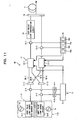
- Fig. 11 is a block diagram showing a light source apparatus 20 according to the second embodiment of the present invention.
- the light source apparatus 20 shown in Fig. 11 differs from that of the first embodiment (see Fig. 1 ) in that the light source apparatus has a redundancy configuration in the form of an optical switch section 17.
- the light source apparatus 20 is identical in configuration with the light source apparatus of the first embodiment. For instance, in the event that an anomaly has arisen in the optical pulse train output from the current optical pulse train generation section 1-1, the optical switch control section 6 switches the current optical pulse train to the optical pulse train output from the backup optical pulse train generation section 1-2.
- the light source apparatus 20 shown in Fig. 11 comprises the optical switch section 17 of redundancy configuration and a switch-to-be-used changeover control section 16 for controlling switching of working light switches in the optical switch section 17 of redundancy configuration.
- the optical switch section 17 is capable of selectively outputting an optical pulse train to be used for generating output light from among the optical pulse trains output from the optical pulse train generation sections 1-1, 1-2, as in the case of the optical switch 3 of the first embodiment.
- the optical switch section 17 comprises 3dB couplers 11-1, 11-2; optical fibers 18-1 to 18-4; two optical switches 12-1, 12-2; tap couplers 13-1, 13-2; and a 3dB coupler 15.
- the 3dB coupler 11-1 is for bifurcating an optical pulse train output from the tap coupler 2-1 into two branches and outputs one of the two branches to the optical switch 12-1 by way of the optical fiber 18-1 and the remaining branch to the optical switch 12-2 by way of the optical fiber 18-2.
- the 3dB coupler 11-2 is for bifurcating an optical pulse train output from the tap coupler 2-2 into two branches and outputs one of the two branches to the optical switch 12-1 by way of the optical fiber 18-3 and the remaining branch to the optical switch 12-2 by way of the optical fiber 18-4.
- the optical switches 12-1, 12-2 function as first and second optical switches which receive the optical pulse trains output from the optical pulse train generation sections 1-1, 1-2 by way of the 3dB couplers 11-1, 11-2 and can selectively output an optical pulse train to be taken for current use among the input optical pulse trains, under control of the optical switch control section 6.
- the optical switch 12-1 for example, is usually used for selecting an optical pulse train.
- the optical switch 12-1 is switched to the other optical switch 12-2, and this optical switch 12-2 can select an optical pulse train.
- the optical switch to be used for selecting an optical pulse train operates in the same manner as does the optical switch 3 of the first embodiment. However, the optical switch not to be used for selecting an optical pulse train is made to output none of the optical pulse trains output from the optical pulse train generation sections 1-1, 1-2.
- the optical switches 12-1, 12-2 of the second embodiment can be configured in the same manner as is the optical switch (see reference numeral 3C) shown in Fig. 4C set forth. If unillustrated gates ⁇ which enable flow/interruption of outputs from the optical switches 12-1, 12-2 upon receipt of a control signal output form the switch-to-be-used changeover control section 16 ⁇ are interposed, by way of modification, between the optical switches 12-1, 12-2 and the tap couplers 13-1, 13-2, the optical switches 12-1, 12-2 can be configured in the same manner as are the optical switches 3A, 3B, 3D and 3E shown in Figs. 4A,4B, 4D and 4E .
- the tap couplers 13-1, 13-2 are provided on optical transmission paths connected to the output sides of the redundancy switches 12-1, 12-2 and bifurcate each of the optical pulse trains selected by the redundancy switches 12-1, 12-2 into two branches. In each case, one of the two branches can be output to the high nonlinear fiber 7, and the other branch can be output to the switch-to-be-used changeover control section 16.
- the 3dB coupler 15 is for guiding the optical pulse train output from the first optical switch 12-1 or the second optical switch 12-2, which is to be used for selecting an optical pulse train, to the high nonlinear fiber 7.
- the switch-to-be-used changeover control section 16 uses the first optical switch 12-1 of the first and second optical switches 12-1, 12-2 in normal times for selectively outputting an optical pulse train taken for current use. In the event that an anomaly has arisen in the optical pulse train output from the first optical switch 12-1, switching between the first optical switch 12-1 and the second optical switch 12-2 is controlled so as to use the second optical switch 12-2 for selectively outputting an optical pulse train to be taken for current use.
- the switch-to-be-used changeover control section 16 comprises a photodiode 16a for converting the current optical pulse train into an electrical signal; an anomaly detection section 16b for detecting an anomaly in the optical pulse train which has been converted into the electrical signal by the photodiode 16a and taken for current use; a timing extraction section 16c for extracting an illumination/extinction timing of the current optical pulse train; and a control signal output section 16d for outputting a control signal to be used for switching a switch to be used to the optical switches 12-1, 12-2 at the timing of extinction extracted by the timing extraction section 16c when the anomaly detection section 16b has detected an anomaly in the current optical pulse train.
- the switch-to-be-used changeover control section 16 monitors an optical pulse train output from the unused optical switch 12-2. When a failure has arisen in the unused optical switch 12-2, an alarm or the like is output without switching the optical switch 12-2 to an optical switch to be used. This prevents a state in which the failure has already arisen in the optical switch to which switching is made, thereby enhancing reliability of switching of a switch to be used.
- a light delay/chirp compensation circuit 14 is provided on the output side of the optical switch 12-1 used in normal times; more specifically, a position between the tap couplers 13-1 and the 3dB coupler 15.
- the optical switch to be used can be switched to the optical switch 12-2 in a preceding stage from when the failure has arisen in the optical switch 12-1 until when a pulse generated after occurrence of the failure is output to the optical coupler 15 and the high nonlinear fiber 7.
- the optical pulse train originating from the optical switch 12-1 can be prevented from being delivered to the optical coupler 15 and the high nonlinear fiber 7 after occurrence of the failure.
- the optical switch to be used is switched between the optical switch 12-1 and the optical switch 12-2 without involvement of instantaneous interruption of power.
- the optical pulse trains generated by the optical pulse train generation sections 1-1, 1-2 can be output to the optical switch 3 after the frequency chirp of the optical pulse trains has been compensated.
- the pulse trains output from the optical pulse train generation sections 1-1, 1-2 are each bifurcated into two branches by the 3dB couplers 11-1, 11-2. Subsequently, the bifurcated pulse trains are input from the current optical pulse train generation section 1-1 and the backup optical pulse train generation section 1-2 to the optical switches 12-1, 12-2 each having a redundancy configuration.
- the outputs from the optical switches 12-1, 12-2 are again coupled together by the coupler 15.
- the optical pulse train output from the coupler 15 is input to the high nonlinear fiber 7 , and the high nonlinear fiber 7 outputs the SC light.
- the optical switch 12-1 to be used for selecting an optical pulse train operates normally (i.e., when the anomaly detection section 16a detects no anomalies)
- the optical pulse train selectively output by the optical switch 12-1 is output to the coupler 15 by way of the light delay/chirp compensation circuit 14.
- the control signal output section 16d When the anomaly detection section 16a has detected occurrence of a failure in the optical switch 12-1 used for selecting an optical pulse train, the control signal output section 16d outputs, to the respective optical switches 12-1, 12-2, a control signal for enabling use of the optical switch 12-2 for selecting the optical pulse train but preventing use of the optical switch 12-1.
- the outputs from the optical switches 12-1, 12-2 are switched during a period of delay time generated by the light delay/chirp compensation circuit 14 connected to a stage subsequent to the switch 12-1. Even when a failure has arisen in the optical switch 12-1, the optical switch to be used can be switched to another optical switch without involvement of instantaneous interruption of power.
- the optical switches 12-1, 12-2 can selectively output any of the optical pulse trains output from the optical switch sections 1-1, 1-2 under control of the optical switch control section 6, as in the case of the first embodiment.
- the second embodiment yields the same advantage as that of the first embodiment. Even when a failure, or the like, has arisen in the first optical switch 12-1 in use, the switch 12-1 can be changed to the second optical switch 12-2 without involvement of instantaneous interruption of power by means of the switch-to-be-sued changeover control section 16 in conjunction with the first and second optical switches 12-1, 12-2. As a result, there is also yielded an advantage of the ability to output the CW light which becomes output light more stably and make an attempt to stabilize operation of the light source apparatus dramatically.
- the light delay/chirp compensation circuit 14 is interposed between the tap coupler 13-1 and the coupler 15.
- the light delay/chirp compensation circuit 14 can be omitted.
- the present embodiment may be provided with a light delay circuit analogous to that shown in Fig. 6 .
- the optical pulse train output from the optical pulse generation section 1-1 is bifurcated into two branches by the 3dB coupler 11-1, and the optical pulse train output from the optical pulse generation section 1-2 is bifurcated into two branches by the 3dB coupler 11-2.
- the thus-bifurcated respective signals are input to the optical switches 12-1, 12-2 each having a redundancy configuration, by way of the optical fibers 18-1 to 18-4.
- the optical switches 12-1, 12-2 shown in Fig. 11 are replaced with an optical switch 12A having optical phase adjustment sections 12a-1, 12a-2 provided at input terminals thereof, thereby enabling correction of a difference between the timings of input pulses attributable to a slight difference in length among the optical fibers 18-1 to 18-4 within the optical switch.
- the optical switch 12A shown in Fig. 12 has a double tandem configuration formed from three optical elements 12b-1 to 12b-3.
- the optical phase adjustment sections 12a-1, 12a-2 are integrated with the optical switch elements 12b-1 to 12b-3 at stages prior to the respective input-side optical switch elements 12b-1, 12b-2.
- the optical phase adjustment sections 12a-1, 12a-2 are formed with electrodes to be used for supplying an electrical signal for phase adjustment to a waveguide formed in a substrate made of, such as lithium niobate or the like.
- the optical phase adjustment sections 12a-1, 12a-2 can perform phase adjustment operation such that the two optical pulse trains input from, e.g., the input ports 12c-1, 12c-2 can be brought in phase with each other.
- the optical phase adjustment sections 12a-1, 12a-2 can correct a difference between a time at which the optical pulse train output from the optical pulse train generation section 1-1 arrives at the optical switch 12A serving as the first optical switch and a time at which the optical pulse train output from the optical pulse train generation section 1-2 arrives at the optical switch 12A serving as the second optical switch.
- any one of the two optical pulse trains whose phases have been adjusted by the optical phase adjustment sections 12a-1, 12a-2 is selectively output from the output port 12d-1 by way of the optical switch elements 12b-1 to 12b-3, as in the case of the optical switch 3E shown in Fig. 4E .
- the other unselected backup optical pulse train can be monitored by way of the output ports 12d-2, 12d-3.
- the output port 12d-1 of the optical switch 12A is constituted as a current optical pulse train output port for outputting an optical pulse train to be taken for current from among the optical pulse trains output from the two optical pulse train generation sections 1-1, 1-2.
- the output ports 12d-2, 12d-3 are constituted as backup optical pulse train output ports to be used for outputting a backup output pulse train other than the current optical pulse train for monitoring purpose.
- the anomaly detection section 16a of the switch-to-be-used changeover control section 16 can determine occurrence of an anomaly in the optical switch 12A serving as both the first and the second optical switches, by means of monitoring a pulse train for backup output from the output ports 12d-2, 12d-3 of the optical switch 12A serving as both the first and the second switches.
- optical switch into which the optical phase adjustment sections 12a-1, 12a-2 are integrated may be substituted by any of the optical switches 3A to 3D shown in Figs. 4A to 4D as well as the optical switch 3E shown in Fig. 4E .
- Fig. 13 is a block diagram showing a light source apparatus 30 according to the third embodiment of the present invention.
- the light source apparatus 30 shown in Fig. 13 differs from the pieces of light source apparatus of the respective embodiments in that the light source apparatus has an optical switch control section 6D for controlling the optical switch 3.
- the light source apparatus 30 is identical with the pieces of light source apparatus of the respective embodiments in that the light source apparatus has the optical pulse train generation sections 1-1, 1-2, the optical switch 3, and the high nonlinear fiber 7.
- the optical switch control section 6D comprises a monitor wavelength filter 2D for extracting, as a monitor wavelength component, a specific wavelength component of the continuous light (SC light) which serves as output light generated by the high nonlinear fiber 7 and has a plurality of wavelengths; a photodiode 4D which is a photoelectric conversion element for converting, into an electrical signal, the monitor wavelength component extracted by the monitor wavelength filter 2D; and an electrical signal processing section 5D for controlling the optical switch 3 on the basis of the electrical signal output from the photodiode 4D.
- SC light continuous light
- the electrical signal processing section 5D comprises a status determination section 5e and the second control signal output section 5f.
- the status determination section 5e receives an electrical signal showing the monitor wavelength component output from the photodiode 4D and determines the status of the optical pulse train output for current use from the optical switch 3 on the basis of variations in the monitor wavelength component. Specifically, the status determination section 5e determines whether or not the monitor wavelength component output from the photodiode 4D has become smaller than a predetermined threshold value and output a result of determination.
- the second control signal output section 5f outputs the second control signal to the optical switch 3 to switch the current optical pulse train output from the optical switch 3 to another optical pulse train without involvement of instantaneous interruption of power. For instance, in a case where the optical switch section 3 outputs, as a current optical pulse train, the optical pulse train generated by the optical pulse train generation section 1-1, when the second control signal is output to the optical switch section 3, the optical pulse train to be output is switched to the optical pulse train generated by the optical pulse train generation section 1-2.
- the high nonlinear fiber 7 generates CW light on the basis of the optical pulse train selected by the optical switch 3 from among the optical pulse trains generated by the optical pulse train generation sections 1-1, 1-2 and outputs the thus-generated CW light.
- the pulse to be input to the optical switch 3 has a narrow width, and difficulty is encountered in monitoring the width of the pulse in real time.
- the band of the WDM signal generated by the high nonlinear fiber 7 undergoes a change, as shown in Figs. 14B-1, 14B-2 .
- the status determination section 5e of the optical switch control section 6D monitors a wavelength component of the CW light output from the high nonlinear fiber 7, the component being susceptible to variations under influence of the width of the signal pulse and not used as a specific signal channel or a communications carrier.
- the optical switch section 3 switches the pulse train before the influence of a change in the pulse affects the signal channel, thereby realizing switching of the pulse train without involvement of instantaneous interruption of power.
- the backup optical pulse train generation section 1-2 can be switched to a current optical pulse train generation section before the optical pulse train being output for current use is completely interrupted.
- the optical pulse train can be switched without involvement of instantaneous interruption of power.
- the current system can be switched to the backup system by means of the optical switch control section 6D through use of the light source apparatus 30 functioning as the SC light source. Therefore, in the event that a failure, or the like, has arisen in the optical pulse train generation section (e.g., the optical pulse train generation section 1-1) of the current system, the optical pulse train can be switched to the optical pulse train output from the optical pulse train generation section (the optical pulse train generation section 1-2) of the backup system without involvement of instantaneous interruption of power.
- the optical pulse train generation section e.g., the optical pulse train generation section 1-1
- the optical pulse train can be switched to the optical pulse train output from the optical pulse train generation section (the optical pulse train generation section 1-2) of the backup system without involvement of instantaneous interruption of power.
- the light source apparatus may have the timing extraction section 5b analogous to that described in connection with the first embodiment and output the second control signal at the timing of extinction extracted by the timing extraction section 5b.
- the two optical pulse train generation sections 1-1, 1-2 are used, wherein one of the two optical pulse train generation sections is used for current use and the other is taken for backup.
- the present invention is not limited to such embodiments.
- Three or more optical pulse generation sections may be prepared, and a combination of the current optical pulse train generation section and the backup optical pulse train generation section may also be embodied as a combination of one or more current optical pulse train generation sections and one or more backup optical pulse train generation sections.
- the present invention can also be embodied as appropriate by combining features of the respective embodiments.
- modifications of the first embodiment can also be combined with the second embodiment.
- the light source apparatus may assume the conf igurat ion described in connection with the second embodiment along with the optical switch control section 6D of the third embodiment.
- the apparatus of the present invention can be manufactured by means of the previously-described embodiments.
Landscapes
- Engineering & Computer Science (AREA)
- Computer Networks & Wireless Communication (AREA)
- Signal Processing (AREA)
- Physics & Mathematics (AREA)
- Electromagnetism (AREA)
- Optical Communication System (AREA)
- Facsimile Scanning Arrangements (AREA)
Claims (12)
- Eine Lichtquellenvorrichtung, umfassend:eine Vielzahl von optischen Pulszugerzeugungsabschnitten (1-1, 1-2), die eine Vielzahl von periodischen optischen Pulszügen erzeugen können, die miteinander synchron sind und die im Wesentlichen gleichen Wiederholungszyklus aufweisen;einen optischer Schaltabschnitt (3, 17), der selektiv einen optischen Pulszug ausgeben kann, der als ein optischer Pulszug zur aktuellen Verwendung unter der Vielzahl von optischen Pulszügen ausgewählt wird, die von der Vielzahl der optischen Pulszugerzeugungsabschnitten (1-1, 1-2) ausgegeben werden;einen Ausgabelichterzeugungsabschnitt (7), der kontinuierliches Licht, das ein vergrößertes Wellenlängenspektrum aufweist, aus dem optischen Pulszug erzeugen kann, der von dem optischen Schaltabschnitt (3, 17) ausgegeben wird; undeinen optischen Schaltsteuerungsabschnitt (6, 6D) zum Steuern des optischen Schaltabschnitts (3, 17) auf solch eine Art und Weise, dass der optische Schaltabschnitt (3, 17) eine Ausgabe von dem optischen Pulszug zur aktuellen Verwendung von dem optischen Schaltabschnitt (3, 17) zur Auslöschungszeit der Vielzahl von optischen Pulszügen schaltet in Übereinstimmung mit den Zuständen der entsprechenden optischen Pulszüge, die durch die Vielzahl von optischen Pulszugerzeugungsabschnitten (1-1, 1-2) erzeugt werden.
- Die Lichtquellenvorrichtung nach Anspruch 1, wobei der optische Schaltsteuerungsabschnitt (6) ferner folgendes umfasst:photoelektrische Konvertierungsabschnitte (4-1, 4-2) zum Konvertieren der entsprechenden optischen Pulszüge, die von der Vielzahl von optischen Pulszugerzeugungsabschnitten (1-1, 1-2) erzeugt werden, in elektrische Signale;einen Anomaliedetektierungsabschnitt (5a) zum Detektieren von Anomalien in den entsprechenden optischen Pulszügen, die durch die photoelektrischen Konvertierungsabschnitte (4-1, 4-2) in elektrische Signale konvertiert wurden;einen Zeitsteuerungsextraktionsabschnitt (5b) zum Extrahieren von Auslöschungs-/Illuminierungszeitsteuerungen der entsprechenden optischen Pulszüge, die durch den photoelektrischen Konvertierungsabschnitt (4-1, 4-2) in elektrische Signale konvertiert wurden; undwobei der erste Steuerungssignalausgabeabschnitt (5c), der, wenn der Anomaliedetektierungsabschnitt (5a) Anomalien in dem optischen Pulszug zur aktuellen Verwendung detektiert hat, das erste Steuerungssignal zu dem optischen Schaltabschnitt (3) ausgibt, um den optischen Pulszug zur aktuellen Verwendung mit einer Auslöschungszeitsteuerung zu schalten, die durch den Zeitsteuerungsextraktionsabschnitt (5b) extrahiert wird.
- Die Lichtquellenvorrichtung nach Anspruch 2, wobei jeder der Vielzahl der optischen Pulszugerzeugungsabschnitte (1-1, 1-2) einen Taktsignalerzeugungsabschnitt (1a) zum Erzeugen eines Taktsignals und eine Pulslichtquelle (1b-1, 1b-2) zum Ausgeben von optischen Pulszügen auf der Basis eines Taktsignals umfasst, das durch den - Taktsignalerzeugungsabschnitt (1a) erzeugt wird; und wobei die Lichtquellenvorrichtung ferner einen Synchronisierungsteuerungsabschnitt umfasst zum synchronen Steuern der Taktsignalerzeugungsabschnitte (1a) der entsprechenden Pulszugerzeugungsäbschnitte (1-1, 1-2) auf der Basis der Auslöschungs-/Illuminierungszeitsteuerungen der entsprechenden optischen Pulszüge, die durch den Zeitsteuerungsextraktionsabschnitt (5b) extrahiert werden.
- Die Lichtquellenvorrichtung nach Anspruch 2, ferner umfassend:Knotenabschnitte, von denen jeder den entsprechenden optischen Pulszug, der von der Vielzahl der optischen Pulszugerzeugungsabschnitte (1-1, 1-2) ausgegeben wird, in zwei Zweige aufteilt, und die einen der Zweige zu dem optischen Schaltabschnitt (3) und den anderen Zweig zu jedem der photoelektrischen Konvertierungsabschnitte (4-1, 4-2) leitet; undeinen Lichtverzögerungsschaltkreis, der zwischen dem Knotenabschnitt und dem optischen Schaltabschnitt (3) eingefügt ist, wobei der Lichtverzögerungsabschnitt die Ausbreitung der entsprechenden optischen Pulszüge verzögert.
- Die Lichtquellenvorrichtung nach Anspruch 2, ferner umfassend:Knotenabschnitte, von denen jeder den entsprechenden optischen Pulszug, der von der Vielzahl der optischen Pulszugerzeugungsabschnitte (1-1, 1-2) ausgegeben wird, in zwei Zweige aufteilt, und die einen der Zweige zu dem optischen Schaltabschnitt (3) und den anderen Zweig zu den entsprechenden photoelektrischen Konvertierungsabschnitte (4-1, 4-2) leitet; undLichtverzögerungsschaltkreise, die jeweils zwischen dem korrespondierenden Knotenabschnitt und dem optischen Schaltabschnitt (3) eingefügt sind, und die die Ausbreitung der entsprechenden optischen Pulszüge verzögern; undChirp-Kompensierungsschaltkreis, der zwischen dem Knotenabschnitt und dem optischen Schalter eingefügt ist, und der Chirp kompensiert.
- Die Lichtquellenvorrichtung nach Anspruch 1, wobeider optische Schaltabschnitt (17) ferner folgendes umfasst:erste und zweite optische Schalter (12-1, 12-2), die von dem optischen Schaltsteuerungsabschnitt (6) gesteuert werden; die optische Pulszüge empfangen, die von der Vielzahl der optischen Pulszugerzeugungsabschnitte (1-1, 1-2) ausgegeben werden; und die selektiv einen optischen Pulszug zur aktuelle Verwendung unter den empfangenen optischen Pulszügen ausgeben können; undeinen Wechselsteuerungsabschnitt (16) für den zu verwendenden Schalter zum Steuern von Schalten zwischen dem ersten optischen Schalter (12-1, 12A) und dem zweiten optischen Schalter (12-2, 12A), so dass der erste optische Schalter (12-1, 12A) bei normalen Zeiten verwendet wird zum selektiven Ausgeben des optischen Pulszugs zur aktuellen Verwendung, und so dass der zweite optische Schalter (12-2, 12A) verwendet wird zum selektiven Ausgeben eines anderen optischen Pulszugs zur aktuellen Verwendung bei dem Ereignis des Auftretens von Anomalien in dem optischen Pulszug zur aktuellen Verwendung, der von dem ersten optischen Schalter (12-1, 12A) ausgegeben wird.
- Die optische Lichtquellenvorrichtung nach Anspruch 6, wobei der erste und der zweite optische Schalter (12A) jeweils folgendes umfassen:einen Ausgabeanschluss (12d-1) für den aktuellen optischen Pulszug zum Ausgeben des optischen Pulszugs zur aktuellen Verwendung unter der Vielzahl der optischen Pulszüge, undAusgabeanschlüsse (12d-2, 12d-3) für optische Sicherungspulszüge zum Ausgegeben eines Sicherungsausgabepulszugs, der sich von dem aktuellen optischen Pulszug unterscheidet, für Überwachungszwecke; und wobeider Wechselsteuerungsabschnitt (16) für den zu verwendenden Schalter konfiguriert ist zum Bestimmen des Auftretens von Anomalien in jedem der ersten und zweiten optischen Schalter (12A) durch Überwachen des Sicherungsausgabepulszuges, der von den Ausgabeanschlüssen (12d-2, 12d-3) für optische Sicherungspulszüge von den entsprechenden ersten und zweiten optischen Schaltern ausgegeben wird.
- Die Lichtquellenvorrichtung nach Anspruch 6, wobei ein Lichtverzögerungsabschnitt (14) eingefügt ist zwischen dem ersten optischen Schalter (12-1) und dem Ausgabelichterzeugungsabschnitt (7) zum Verzögern der Ausbreitung eines optischen Pulszuges, der von dem ersten optischen Schalter (12-1) ausgegeben wird.
- Die Lichtquellenvorrichtung nach Anspruch 6, wobei ein Lichtverzögerungsabschnitt (14) zum Verzögern der Ausbreitung eines optischen Pulszuges, der von dem ersten optischen Schalter (12-1) ausgegeben wird, und ein Chirp-Kompensierungsschaltreis (14) zum Bewirken von Chirp-Kompensierung eingefügt sind zwischen dem ersten optischen Schalter und dem Ausgabelichterzeugungsabschnitt.
- Die Lichtquellenvorrichtung nach Anspruch 6, ferner umfassend:einen Lichtphaseneinstellungsabschnitt (12a-1, 12a-2) zum Kompensieren einer Differenz zwischen einer Zeit, wenn von der Vielzahl von optischen Pulszügen ausgegebene entsprechende optische Pulszüge an dem ersten optischen Schalter (12A) ankommen, und einer Zeit, wenn von der Vielzahl von optischen Pulszügen ausgegebene entsprechende optische Pulszüge an dem zweiten optischen Schalter (12A) ankommen.
- Die Lichtquellenvorrichtung nach Anspruch 1, wobei der optische Schaltsteuerungsabschnitt (6D) folgendes umfasst:einen Statusbestimmungsabschnitt (5e) zum Bestimmen des Status eines optischen Pulszuges, der ausgegeben wird zur aktuellen Verwendung von dem optischen Schaltabschnitt (3), auf der Basis von Variationen in einer spezifischen Wellenlängenkomponente in kontinuierlichem Licht mit mehreren Wellenlängen, die als das Ausgabelicht erzeugt werden durch den Ausgabelichterzeugungsabschnitt (7); undder zweite Steuerungssignalausgabeabschnitt (5f) zum Ausgegeben des zweiten Steuerungssignals zu dem optischen Schalter (3), um eine Ausgabe des optischen Pulszuges zur aktuellen Verwendung von dem optischen Schaltabschnitt (3) zu schalten ohne Involvierung von direkter Leistungsunterbrechung, wenn der Statusbestimmungsabschnitt (5e) bestimmt, dass der Status des optischen Pulszuges, der ausgegeben wird zur aktuellen Verwendung von dem optischen Schaltabschnitt (3), anomal ist.
- Ein Verfahren zur redundanten Schaltung einer Lichtquelle unter Verwendung eines Ausgabelichterzeugungsabschnitts (7), der kontinuierliches Licht erzeugen kann, das ein vergrößertes Wellenlängenspektrum (WC) aufweist, als Ausgabelicht von einem periodischen optischen Pulszug, wobei das Verfahren folgendes umfasst:Verwenden einer Vielzahl von optischen Pulszugerzeugungsabschnitte (1-1, 1-2), die eine Vielzahl von periodischen optischen Pulszügen erzeugen können, die miteinander synchron sind und die im wesentlichen gleiche Wiederholungszyklen aufweisen;Auswählen jeglicher der Vielzahl von optischen Pulszugerzeugungsabschnitten (1-1, 1-2) zur aktuellen Verwendung und Bewirken, dass der Ausgabelichterzeugungsabschnitt (7) das Ausgabelicht erzeugt von dem periodischen optischen Pulszug, der von dem ausgewählten optischen Pulszugerzeugungsabschnitt ausgegeben wird, zur aktuellen Verwendung; undSchalten, unter der Vielzahl von optischen Pulszugerzeugungsabschnitten (1-1, 1-2), von jedem der optischen Pulszugerzeugungsabschnitte, die nicht verwendet werden zur aktuellen Verwendung, zur aktuellen Verwendung, wobei die Zeit zum Schalten des optischen Pulszugerzeugungsabschnitts zur aktuellen Verwendung zu einer Auslöschungszeitsteuerung der Vielzahl von optischen Pulszügen auftritt, und Bewirken, dass der Ausgabelichterzeugungsabschnitt (7) das Ausgabelicht von dem periodischen optischen Pulszug erzeugt, der von dem optischen Pulszugerzeugungsabschnitt (1-1, 1-2) ausgegeben wird, der zur aktuellen Verwendung geschaltet ist.
Applications Claiming Priority (2)
| Application Number | Priority Date | Filing Date | Title |
|---|---|---|---|
| JP2004096023A JP4478492B2 (ja) | 2004-03-29 | 2004-03-29 | 光源装置および光源装置の冗長切り替え方法 |
| JP2004096023 | 2004-03-29 |
Publications (3)
| Publication Number | Publication Date |
|---|---|
| EP1583259A2 EP1583259A2 (de) | 2005-10-05 |
| EP1583259A3 EP1583259A3 (de) | 2006-02-01 |
| EP1583259B1 true EP1583259B1 (de) | 2009-01-21 |
Family
ID=34879917
Family Applications (1)
| Application Number | Title | Priority Date | Filing Date |
|---|---|---|---|
| EP04016462A Expired - Lifetime EP1583259B1 (de) | 2004-03-29 | 2004-07-13 | Lichtquellenvorrichtung und Verfahren zur redundanten Schaltung dieser Lichtquelle |
Country Status (4)
| Country | Link |
|---|---|
| US (1) | US7447446B2 (de) |
| EP (1) | EP1583259B1 (de) |
| JP (1) | JP4478492B2 (de) |
| DE (1) | DE602004019181D1 (de) |
Families Citing this family (19)
| Publication number | Priority date | Publication date | Assignee | Title |
|---|---|---|---|---|
| JP4569761B2 (ja) * | 2005-03-08 | 2010-10-27 | 日本電気株式会社 | 光送信器、光伝送システム、および光中継器 |
| CN101212254A (zh) | 2006-12-27 | 2008-07-02 | 华为技术有限公司 | 一种光源链路传输装置和方法 |
| BRPI0909474A2 (pt) * | 2008-03-28 | 2015-12-29 | Nortel Networks Ltd | fonte de luz protegida para múltiplas redes ópticas passivas multiplexadas por divisão de comprimento de onda (wdm-pons) |
| JP5787414B2 (ja) | 2009-12-03 | 2015-09-30 | ムーグ インコーポレーテッド | 光ファイバ・ロータリージョイント、それによって実施される方法、及び光ファイバデバイス |
| JP2011142584A (ja) * | 2010-01-08 | 2011-07-21 | Fujitsu Optical Components Ltd | 光伝送装置 |
| CZ302947B6 (cs) * | 2010-09-02 | 2012-01-25 | CESNET, zájmové sdružení právnických osob | Modulární stavebnice zarízení pro variabilní distribuci, smešování a monitoring optických signálu v Internetu a jiných sítích |
| JP5970943B2 (ja) * | 2012-05-01 | 2016-08-17 | 富士通株式会社 | 光伝送装置、及び光伝送方法 |
| US9900085B2 (en) * | 2015-03-18 | 2018-02-20 | Finisar Corporation | Sparing configurations and protocols for parallel fiber optics |
| KR102064791B1 (ko) * | 2015-04-23 | 2020-03-02 | 한국전자통신연구원 | 광전달망 시스템에서의 데이터 손실을 최소화하는 보호절체 장치 및 방법 |
| JP6438426B2 (ja) * | 2016-03-30 | 2018-12-12 | Seiオプティフロンティア株式会社 | 光切替ユニット及び光切替装置 |
| US10313019B2 (en) * | 2016-07-01 | 2019-06-04 | Luxtera, Inc. | Method and system for redundant light sources by utilizing two inputs of an integrated modulator |
| KR102338923B1 (ko) | 2017-07-06 | 2021-12-14 | 삼성전자주식회사 | 광 집적 회로 및 광 전송기 |
| US10199918B2 (en) * | 2017-07-10 | 2019-02-05 | Semiconductor Components Industries, Llc | Method of forming a semiconductor device |
| US10725240B2 (en) * | 2018-09-14 | 2020-07-28 | Cisco Technology, Inc. | Laser sparing for photonic chips |
| CN111147130B (zh) * | 2018-11-02 | 2023-05-09 | 华为技术有限公司 | 光源备份方法、装置以及系统 |
| CN114879320A (zh) * | 2019-06-03 | 2022-08-09 | 华为技术有限公司 | 光源切换方法和装置 |
| JP7524686B2 (ja) * | 2020-09-09 | 2024-07-30 | 日本電気株式会社 | 光伝送装置、光伝送方法、及びプログラム |
| US20250189864A1 (en) * | 2023-12-08 | 2025-06-12 | Nvidia Corp. | Laser sparing architectures for multi-wavelength laser arrays |
| JP7814603B1 (ja) * | 2025-08-28 | 2026-02-16 | Nttイノベーティブデバイス株式会社 | 光源装置 |
Family Cites Families (7)
| Publication number | Priority date | Publication date | Assignee | Title |
|---|---|---|---|---|
| JPH09244076A (ja) * | 1996-03-08 | 1997-09-19 | Toshiba Corp | 多波長光源 |
| JP3605629B2 (ja) | 1998-12-15 | 2004-12-22 | 富士通株式会社 | 光源の冗長切替方法及び該方法による波長多重伝送装置 |
| US6480656B1 (en) | 1999-02-19 | 2002-11-12 | The Regents Of The University Of Michigan | Method and system for generating a broadband spectral continuum, method of making the system and pulse-generating system utilizing same |
| JP2001339344A (ja) | 2000-05-29 | 2001-12-07 | Hitachi Ltd | 光信号切替装置 |
| JP4762434B2 (ja) | 2001-04-23 | 2011-08-31 | 古河電気工業株式会社 | 光回路の作製方法 |
| US7127168B2 (en) * | 2001-06-13 | 2006-10-24 | Nippon Telegraph And Telephone Corporation | Multi-wavelength optical modulation circuit and wavelength-division multiplexed optical signal transmitter |
| KR100496710B1 (ko) * | 2002-01-21 | 2005-06-28 | 노베라옵틱스코리아 주식회사 | 주입된 비간섭성 광에 파장 잠김된 광원을 이용한 양방향파장분할다중방식 수동형 광 네트워크 |
-
2004
- 2004-03-29 JP JP2004096023A patent/JP4478492B2/ja not_active Expired - Fee Related
- 2004-07-08 US US10/885,755 patent/US7447446B2/en not_active Expired - Lifetime
- 2004-07-13 EP EP04016462A patent/EP1583259B1/de not_active Expired - Lifetime
- 2004-07-13 DE DE602004019181T patent/DE602004019181D1/de not_active Expired - Lifetime
Also Published As
| Publication number | Publication date |
|---|---|
| EP1583259A3 (de) | 2006-02-01 |
| US20050213972A1 (en) | 2005-09-29 |
| JP2005286581A (ja) | 2005-10-13 |
| US7447446B2 (en) | 2008-11-04 |
| JP4478492B2 (ja) | 2010-06-09 |
| EP1583259A2 (de) | 2005-10-05 |
| DE602004019181D1 (de) | 2009-03-12 |
Similar Documents
| Publication | Publication Date | Title |
|---|---|---|
| US7447446B2 (en) | Light source apparatus, and method for switching redundancy of the light source | |
| US6532091B1 (en) | Optical digital regenerator | |
| JP3975810B2 (ja) | 光片側サイドバンド送信器 | |
| US20030175033A1 (en) | Optical transmission system, optical transmitter and methods thereof | |
| US6778730B2 (en) | Optical signal processing device | |
| JPH09244076A (ja) | 多波長光源 | |
| CN101312383A (zh) | 光传输设备、光传输系统与光终端站 | |
| US20030020985A1 (en) | Receiver for high-speed optical signals | |
| GB2460483A (en) | Determining the type of an optical fibre from measured delay-time differences between pulse signals of different wavelengths | |
| US8396362B2 (en) | Light transmitting and receiving module, method for managing the same, light transmitting and receiving apparatus, and wavelength-multiplexing light transmitting and receiving apparatus | |
| US6396607B1 (en) | Multi-wavelength all-optical regenerators (MARS) | |
| US7006771B1 (en) | Optical communication apparatus and optical add/drop apparatus | |
| US11496213B2 (en) | Fast probing of signal quality in a WDM network | |
| US11309973B2 (en) | Optical burst monitoring | |
| US9712248B2 (en) | Optical transmission device and optical transmission method | |
| JP3740538B2 (ja) | 光受信装置及び分散補償制御方法 | |
| JP5899866B2 (ja) | 光中継増幅装置及び方法 | |
| US20200200973A1 (en) | Wavelength conversion device and excitation light switching method | |
| Barry et al. | A high-speed optical star network using TDMA and all-optical demultiplexing techniques | |
| WO2001004677A1 (en) | Optical data format converter | |
| JP2004221968A (ja) | 光伝送方式 | |
| JP2011146787A (ja) | 光通信装置 | |
| JP6300504B2 (ja) | 光回線障害検出装置、光/無線回線切替装置および光伝送システム | |
| JPH0946735A (ja) | 光クロスコネクト方法および該方法を用いた光クロスコネクト装置 | |
| JPH11225109A (ja) | 光伝送装置及び光信号送出方法 |
Legal Events
| Date | Code | Title | Description |
|---|---|---|---|
| PUAI | Public reference made under article 153(3) epc to a published international application that has entered the european phase |
Free format text: ORIGINAL CODE: 0009012 |
|
| AK | Designated contracting states |
Kind code of ref document: A2 Designated state(s): AT BE BG CH CY CZ DE DK EE ES FI FR GB GR HU IE IT LI LU MC NL PL PT RO SE SI SK TR |
|
| AX | Request for extension of the european patent |
Extension state: AL HR LT LV MK |
|
| PUAL | Search report despatched |
Free format text: ORIGINAL CODE: 0009013 |
|
| AK | Designated contracting states |
Kind code of ref document: A3 Designated state(s): AT BE BG CH CY CZ DE DK EE ES FI FR GB GR HU IE IT LI LU MC NL PL PT RO SE SI SK TR |
|
| AX | Request for extension of the european patent |
Extension state: AL HR LT LV MK |
|
| 17P | Request for examination filed |
Effective date: 20060208 |
|
| 17Q | First examination report despatched |
Effective date: 20060809 |
|
| AKX | Designation fees paid |
Designated state(s): BG DE FR |
|
| RBV | Designated contracting states (corrected) |
Designated state(s): DE FR GB |
|
| GRAP | Despatch of communication of intention to grant a patent |
Free format text: ORIGINAL CODE: EPIDOSNIGR1 |
|
| GRAS | Grant fee paid |
Free format text: ORIGINAL CODE: EPIDOSNIGR3 |
|
| GRAA | (expected) grant |
Free format text: ORIGINAL CODE: 0009210 |
|
| AK | Designated contracting states |
Kind code of ref document: B1 Designated state(s): DE FR GB |
|
| REG | Reference to a national code |
Ref country code: GB Ref legal event code: FG4D |
|
| REF | Corresponds to: |
Ref document number: 602004019181 Country of ref document: DE Date of ref document: 20090312 Kind code of ref document: P |
|
| PLBE | No opposition filed within time limit |
Free format text: ORIGINAL CODE: 0009261 |
|
| STAA | Information on the status of an ep patent application or granted ep patent |
Free format text: STATUS: NO OPPOSITION FILED WITHIN TIME LIMIT |
|
| 26N | No opposition filed |
Effective date: 20091022 |
|
| REG | Reference to a national code |
Ref country code: FR Ref legal event code: PLFP Year of fee payment: 13 |
|
| REG | Reference to a national code |
Ref country code: FR Ref legal event code: PLFP Year of fee payment: 14 |
|
| REG | Reference to a national code |
Ref country code: FR Ref legal event code: PLFP Year of fee payment: 15 |
|
| PGFP | Annual fee paid to national office [announced via postgrant information from national office to epo] |
Ref country code: FR Payment date: 20200611 Year of fee payment: 17 |
|
| PGFP | Annual fee paid to national office [announced via postgrant information from national office to epo] |
Ref country code: GB Payment date: 20200701 Year of fee payment: 17 Ref country code: DE Payment date: 20200630 Year of fee payment: 17 |
|
| REG | Reference to a national code |
Ref country code: DE Ref legal event code: R119 Ref document number: 602004019181 Country of ref document: DE |
|
| GBPC | Gb: european patent ceased through non-payment of renewal fee |
Effective date: 20210713 |
|
| PG25 | Lapsed in a contracting state [announced via postgrant information from national office to epo] |
Ref country code: GB Free format text: LAPSE BECAUSE OF NON-PAYMENT OF DUE FEES Effective date: 20210713 Ref country code: DE Free format text: LAPSE BECAUSE OF NON-PAYMENT OF DUE FEES Effective date: 20220201 |
|
| PG25 | Lapsed in a contracting state [announced via postgrant information from national office to epo] |
Ref country code: FR Free format text: LAPSE BECAUSE OF NON-PAYMENT OF DUE FEES Effective date: 20210731 |