EP1583254B1 - Diplexeur et circuit d'adapation - Google Patents
Diplexeur et circuit d'adapation Download PDFInfo
- Publication number
- EP1583254B1 EP1583254B1 EP04007634A EP04007634A EP1583254B1 EP 1583254 B1 EP1583254 B1 EP 1583254B1 EP 04007634 A EP04007634 A EP 04007634A EP 04007634 A EP04007634 A EP 04007634A EP 1583254 B1 EP1583254 B1 EP 1583254B1
- Authority
- EP
- European Patent Office
- Prior art keywords
- band
- antenna port
- branch
- impedance
- circuit
- Prior art date
- Legal status (The legal status is an assumption and is not a legal conclusion. Google has not performed a legal analysis and makes no representation as to the accuracy of the status listed.)
- Expired - Lifetime
Links
- 239000003990 capacitor Substances 0.000 claims description 25
- 230000001939 inductive effect Effects 0.000 claims description 11
- 238000010586 diagram Methods 0.000 description 7
- 230000000694 effects Effects 0.000 description 3
- 238000012545 processing Methods 0.000 description 3
- 230000005540 biological transmission Effects 0.000 description 2
- 230000001413 cellular effect Effects 0.000 description 2
- 238000012938 design process Methods 0.000 description 2
- 238000003780 insertion Methods 0.000 description 2
- 230000037431 insertion Effects 0.000 description 2
- 201000008217 Aggressive systemic mastocytosis Diseases 0.000 description 1
- 239000000919 ceramic Substances 0.000 description 1
- 238000007796 conventional method Methods 0.000 description 1
- 230000008878 coupling Effects 0.000 description 1
- 238000010168 coupling process Methods 0.000 description 1
- 238000005859 coupling reaction Methods 0.000 description 1
- 230000000593 degrading effect Effects 0.000 description 1
- 230000001419 dependent effect Effects 0.000 description 1
- 238000013461 design Methods 0.000 description 1
- 230000001627 detrimental effect Effects 0.000 description 1
- 230000001771 impaired effect Effects 0.000 description 1
- 238000012552 review Methods 0.000 description 1
- 238000000926 separation method Methods 0.000 description 1
Images

Classifications
-
- H—ELECTRICITY
- H04—ELECTRIC COMMUNICATION TECHNIQUE
- H04B—TRANSMISSION
- H04B1/00—Details of transmission systems, not covered by a single one of groups H04B3/00 - H04B13/00; Details of transmission systems not characterised by the medium used for transmission
- H04B1/02—Transmitters
- H04B1/04—Circuits
- H04B1/0458—Arrangements for matching and coupling between power amplifier and antenna or between amplifying stages
-
- H—ELECTRICITY
- H04—ELECTRIC COMMUNICATION TECHNIQUE
- H04B—TRANSMISSION
- H04B1/00—Details of transmission systems, not covered by a single one of groups H04B3/00 - H04B13/00; Details of transmission systems not characterised by the medium used for transmission
- H04B1/005—Details of transmission systems, not covered by a single one of groups H04B3/00 - H04B13/00; Details of transmission systems not characterised by the medium used for transmission adapting radio receivers, transmitters andtransceivers for operation on two or more bands, i.e. frequency ranges
- H04B1/0053—Details of transmission systems, not covered by a single one of groups H04B3/00 - H04B13/00; Details of transmission systems not characterised by the medium used for transmission adapting radio receivers, transmitters andtransceivers for operation on two or more bands, i.e. frequency ranges with common antenna for more than one band
Definitions
- the present invention relates to signal separating devices.
- the invention relates particularly, but not exclusively, to a signal separating device for use at the antenna of a multi-band telecommunications device, for example a mobile (or cellular) telephone handset.
- a multiplexer is a multi-port frequency dependent device that may be used as a separator or combiner of signals falling in different frequency bands.
- the most common type of multiplexer is a three port device known as a diplexer.
- the respective transmit (TX) and receive (RX) circuitry for each operational frequency band usually share a common antenna.
- a diplexer circuit is typically used to electrically couple the respective transmit (TX) and receive (RX) circuitry to the antenna. The diplexer ensures that signals in a given frequency band are not directed to the circuitry for a different frequency band.
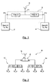
- FIG. 1 shows a simplified block diagram of part of a conventional dual-band telecommunications device such as may be found in a mobile telephone handset. It is assumed that the device is intended for operation in two frequency bands A and B. Hence, the device includes respective TX/RX circuitry 2, 4 for bands A and B respectively, an antenna 6 and a conventional diplexer 8.
- the diplexer 8 comprises three ports P1, P2 and P3. P1 is connected to the antenna 6, P2 is connected to the TX/RX circuitry of band A and P3 is connected to the TX/RX circuitry of band B.
- the diplexer 8 comprises two circuit branches, a first between P1 and P2, and a second between P1 and P3.
- the first branch includes a filter (Filter A) for passing signals in frequency band A.
- the second branch includes a filter (Filter B) for passing signals in frequency band B.
- Each branch may also include one or more impedance matching components (not individually shown in Figure 1 ) to provide in-band impedance matching.
- the arrangement is such that, when a signal in frequency band A is received by antenna 6, Filter A allows the received signal to pass from P1 to P2 and thereby on to the band A TX/RX circuitry 2, while Filter B prevents the received signal from passing from P1 to P3. Similarly, when a signal in frequency band B is received by antenna 6, Filter B allows the received signal to pass from P1 to P3 and thereby on to the band B TX/RX circuitry 4, while Filter A prevents the received signal from passing from P1 to P2.
- in-band is intended to refer to the components or characteristics of a circuit or system that relate to the selected or active operational frequency band.
- the term “out-of-band” is intended to refer to the components or characteristics of a circuit or system that relate to an operational frequency band other than the selected or active operational frequency band.
- the diplexer branch between P1 and P2 may be said to be the in-band branch, whereas the branch between P1 and P3 may be said to be the,out-of-band branch.
- the out-of-band branch of the diplexer 8 should present an open-circuit to the antenna port P1.
- the out-of-band branch often presents, to the antenna port P1, a finite capacitive or inductive impedance with a high reflection coefficient.
- the high reflection coefficient enables the out-of-band branch to perform the basic function of preventing the received signal from travelling along the out-of-band branch.
- the finite impedance is commonly relatively low and this is detrimental to the performance of the diplexer and to the device of which it is part (as measured for example, by voltage standing wave ration (VSWR) and insertion loss (IL)).
- EP 0 872 953 discloses a branch filter having the features recited in the precharacterising portion of claim 1.
- EP 0 872 953 uses a series inductor and a series capacitor at the antenna port to provide out-of-band impedance matching, and does not provide any protection from ESD.
- a first aspect of the invention provides a signal separating device as claimed in claim 1.
- the impedance matching circuit comprises an inductor connected between the antenna port and electrical ground. This provides ESD protection at the antenna port.
- the first and second circuit branches are provided between the antenna port and a second and third port respectively, and a respective series capacitor is provided at each of said second and third ports.
- This provides DC decoupling from DC bias signals which may be used in the associated TX/RX circuitry.
- at least one circuit branch includes a series capacitor at the antenna port in order to provide DC decoupling at the antenna port.
- the invention is not limited to signal separating devices having two circuit branches (e.g. a diplexer) but may also provide signal separating devices having three or more circuit branches and three or more corresponding operational frequency bands.
- a second aspect of the invention provides an antenna switch module, or equivalent device, comprising a signal separating device according to the first aspect of the invention.
- the invention is described and illustrated in the context of a diplexer. It will be understood that the invention is not limited to diplexers and may alternatively be employing with triplexers, multiplexers, or similar signal separating devices.
- FIG. 10 there is shown generally indicated as 10, a simplified block diagram of part of a dual-band telecommunications device such as may be found in a mobile telecommunications handset.
- the circuitry shown in Figure 2 is sometimes referred to as an antenna switch module (ASM), particularly when incorporated into a single module.
- the ASM 10 is generally similar to that illustrated in Figure 1 , although the TX and RX circuitry is shown in more detail.
- the ASM 10 includes TX/RX circuitry 12 for a first operational frequency band A and TX/RX circuitry 14 for a second operational frequency band B.
- the TX/RX circuitry 12, 14 are each electrically coupled to an antenna 16 by a diplexer circuit, or diplexer 18.
- the diplexer 18 has an antenna port P1 connected to the antenna 16, a second port P2 connected to TX/RX circuitry 12 and a third port P3 connected to TX/RX circuitry 14.
- the TX/RX circuitry 12 for band A includes a first port TX_A for receiving signals in frequency band A from signal generating circuitry (not shown) and a second port RX_A for providing signals received at antenna 16 in frequency band A to signal processing circuitry (not shown).
- a third port VC_A is provided for receiving a control signal, typically in the form of an ON/OFF D.C. voltage, for selecting the setting of a switching device 20_A.
- switching device 20_A selects either to electrically connect TX_A to port P2 of the diplexer 18 (thereby allowing signals in band A to be transmitted via antenna 16 while simultaneously electrically isolating RX_A and associated circuitry from P2) or to electrically connect RX_A to port P2 of the diplexer 18 (thereby allowing signals in band A received at antenna 16 to be providing to the signal processing circuitry, while simultaneously electrically isolating TX_A and associated circuitry from P2).
- a first filter 22_A may be provided between the TX_A port and the switching device 20_A for removing harmonics of the signal to be transmitted.
- a second filter 24_A may be provided between the RX_A port and the switching device 20_A for preventing signals received at TX_A from reaching RX_A. Commonly, filter 24_A is included in switching device 20_A.
- TX/RX circuitry 14 is generally similar in structure and operation to TX/RX circuitry 12 and includes a first port TX_B for receiving signals in frequency band B from signal generating circuitry (not shown), a second port RX_B for providing signals received at antenna 16 in frequency band B to signal processing circuitry (not shown) and a third port VC_B for receiving a control signal for selecting the setting of switching device 20_B.
- a first filter 22_B may be provided between the TX_B port and the switching device 20_B for removing harmonics of the signal to be transmitted and a second filter 24_B may be provided between the RX_B port and the switching device 20_B for preventing signals received at TX_B from reaching RX_B.
- signal paths in the ASM 10 are provided by, where appropriate, transmission lines, for example microstrip transmission lines.
- ASM 10 The specific structure of the ASM 10, and in particular the TX/RX circuitry 12, 14, is given by way of example only. There are many different conventional architectures for ASMs, or similar devices, which include a diplexer, or similar device, at the antenna. The invention is not limited to use with the specific architecture shown in Figure 2 .
- the ASM 10 suffers from poor out-of-band matching as outlined above.
- FIG 3 shows a block diagram of a signal separating device in the form of a diplexer 118 embodying the present invention.
- Diplexer 118 is generally similar to the diplexer 8 presented in Figure 1 but further includes an impedance matching circuit 130 at the antenna port P1. Because of its location at the antenna port P1, the impedance matching circuit 130 may be said to be common to both branches of the diplexer 118.
- the impedance matching circuit 130 is arranged so that, when signals are received in one or other of the operational frequency bands, the impedance matching circuit matches or tunes out any reactive (i.e. capacitive or inductive) components of the impedance presented to the antenna port P1 by the out-of-band branch.
- the impedance matching circuit 130 is arranged so that the impedance, or more particularly the reactance, it presents to the antenna port P1 is substantially the opposite of the reactance presented to the antenna port P1 by the out-of-band diplexer branch, e.g. if the reactance presented to the antenna port P1 by the out-of-band diplexer branch is capacitive, then the reactance the impedance matching circuit presents to the antenna port P1 is correspondingly inductive, and vice versa, so that the combined reactance at P1 is substantially zero.
- the impedance matching circuit comprises an inductor provided between antenna port P1 and electrical ground (earth), as is illustrated in Figure 4 .
- Diplexer 218 comprising a specific embodiment of the general diplexer architecture 118 shown in Figure 3 .
- Diplexer 218 comprises an antenna port P1, a second port P2 for connection to the TX/RX circuitry (not shown) of a first operational frequency band (Band A), and a third port P3 for connection to the TX/RX circuitry (not shown) of a second operational frequency band (Band B).
- the diplexer circuit branch between ports P1 and P2 comprises a filter circuit 132 which allows signals in Band A to pass from antenna port P1 to port P2 while preventing signals in Band B from doing so.
- This branch is hereinafter referred to as the Band A branch and may be said to be in-band when signals are received in Band A, and out-of-band when signals are received in Band B.
- the diplexer circuit branch between ports P1 and P3 comprises a filter circuit 134 which allows signals in Band B to pass from antenna port P1 to port P3 while preventing signals in Band A from doing so.
- This branch is hereinafter referred to as the Band B branch and may be said to be in-band when signals are received in Band B, and out-of-band when signals are received in Band A.
- operational frequency Band A is centred around approximately 890 MHz (and may therefore be referred to as the low band) and that operational frequency Band B is centred around approximately 1850 MHz (and may therefore be referred to as the high band).
- These frequency bands are commonly used in cellular telecommunications and are usually referred to as a GSM band and DCS band respectively.
- the architecture of filter 132 is of a general notch, or bandstop, type filter and comprises a resonator 136 comprising an inductor L1 and capacitor C1 in parallel with one another and in series with the circuit branch between P1 and P2.
- the component values for L1 and C1 are selected so that resonator 136 resonates in frequency Band B.
- resonator 136 presents a substantially open-circuit to signals received at the antenna port P1 in Band B.
- the Band A branch is in-band it behaves as a matched through-line and signals in Band A are allowed to pass from P1 to P2.
- one or more in-band matching components are required so that the Band A branch, when in-band, is matched to the characteristic impedance of the system. This may be achieved by any conventional technique, for example by adding one or more reactive components which transform the in-band impedance of the Band A branch, as presented to P1, to the centre point of a conventional Smith Chart).
- Band B is centred around 1850 MHz
- This causes the resonator 136 to present an inductive impedance to P1 when in band and so a capacitive in-band matching component in the form of capacitor Cc is required.
- a capacitor in series with the diplexer branch in order to provide D.C. decoupling.
- series capacitor Cc is preferably provided at port P2.
- a suitable value for Cc is approximately 4.46pF.
- Filter 132 also includes an additional capacitance which, in the present example, comprises a capacitor C2 connected between the Band A branch and electrical ground, i.e. a shunt capacitor.
- capacitor C2 is to adjust the reactance presented to P1 by the Band A branch when out-of-band, as is described in more detail below.
- the architecture of filter 134 in the Band B branch is of a general notch, or bandstop, type filter and comprises a resonator 138 comprising an inductor L3 and a capacitor C3 in series with one another and in parallel, or shunt, with the circuit branch between P1 and P3.
- the component values L3 and C3 selected so that resonator 138 resonates in Band A.
- resonator 138 acts as a short-circuit to signals in Band A and so prevents such signals from reaching port P3.
- Band B branch is in-band it behaves as a matched through-line and signals in Band B are allowed to pass from P1 to P3.
- one or more in-band matching components are usually required to match the in-band impedance of the Band A branch to the characteristic impedance of the system.
- the resulting in-band impedance presented at P1 is inductive and so one or more in-band matching components having a capacitive reactance are required.
- the required corrective reactance, and hence component values, may conveniently be determined using a conventional Smith Chart.
- a shunt capacitor may be employed, but it is preferred to use at least one capacitor in series with the circuit branch in order to provide D.C. decoupling.
- capacitor Ca is located between the resonator 138 and P1
- capacitor Cb is located between the resonator 138 and P3.
- suitable values for each of capacitors Ca and Cb are 1.47 pf or 2.01 pF.
- Capacitor Ca provides DC decoupling at the antenna port P1 while Cb provides DC decoupling at P3 to block the DC bias (not shown) which may be used for the TX/RX switching diodes.
- the out-of-band impedance presented to the antenna port P1 by the Band B diplexer branch of Figure 4 is capacitive.
- filter 138 behaves as a capacitor connected between P1 and ground rather than behaving as an open-circuit (as is desired).
- the effective out-of-band impedance presented to P1 by the Band B branch is found to be approximately -j1.792.
- the Band B branch causes, when out-of-band, an impedance mismatch at the antenna port P1 and at the output port P2.
- the configuration of the Band A branch is such that, when out-of-band, it presents a substantially open-circuit to P1, i.e. there is no significant reactive impedance presented to P1.
- the Band A branch does not have a significant affect on the in-band performance of the Band B branch.
- stray capacitance to electrical ground may be present and this may cause the out-of-band Band A branch to present a capacitive reactance at P1.
- the role of the impedance matching circuit 130 is to tune out, or cancel, the effect of the out-of-band impedance, and in particular the reactive component of the out-of-band-impedance, presented at the antenna port P1 by one or both of the diplexer branches.
- the Band B branch presents a reactive out-of-band impedance at P1. Since the reactive component of this out-of-band impedance is capacitive, an inductive matching network 130 is required.
- the matching network 130 comprises an inductor Le connected between the antenna port P1 and electrical ground. However, the presence of inductor Le upsets the otherwise open-circuit out-of-band characteristic of the Band A branch.
- the out-of-band impedance of the Band A branch is deliberately made to be reactive (capacitive in the present example) to an extent that will be tuned out by the matching circuit 130 (in this case the inductor Le).
- the respective out-of-band reactances of the diplexer branches must be carefully selected in order that they may each be tuned out, or cancelled, by a single matching circuit 130.
- the respective out-of-band reactance of each diplexer branch is arranged so that it may be characterised as a capacitance or an inductance connected between the antenna port P1 and electrical ground.
- Z is impedance
- R is the resistive component
- X is the reactive component.
- the out-of-band impedances of the Band A and Band B branches, Z A , Z B are made to be reactive, with a high reflection coefficient and with a carefully selected ratio between the respective reactive components X A , X B .
- the respective resistive components R A , R B are very small (typically less than 0.1 normalised value) and are therefore ignored.
- the out-of-band reactances are comprised of shunt capacitances C A , C B and the matching circuit 130 comprises a shunt inductance Le, when signals are received in band A, Le is selected to resonate with C B , and when signals are received in band B, Le is selected to resonate with C A .
- F A 1 / 2 ⁇ ⁇ LeC B
- F B 1 / 2 ⁇ ⁇ LeC A
- F A and F B are frequencies, conveniently mid-band frequencies, representing operational frequency bands A and B respectively.
- the reactances X A , X B and the reactance of the matching circuit 130 are chosen so that the following criteria are met: when receiving signals in Band A, the reactance of the matching circuit 130 is substantially the opposite of the reactance presented to the antenna port P1 by the Band B diplexer branch; and, when receiving signals in Band B, the reactance of the matching circuit 130 is substantially the opposite of the reactance presented to the antenna port P1 by the Band A diplexer branch.
- the arrangement is such that the inductor Le resonates, in each operational frequency band A and B, together with the effective capacitance presented to the antenna port P1 by the out-of-band branch.
- the combination of the inductor Le and out-of-band branch present a very high impedance (substantially open-circuit) at the antenna port P1.
- the performance of the in-band branch is not affected by the out-of-band branch since the impedance mismatch caused by the reactive out-of-band branch has been tuned out by the addition of the inductor Le.
- the value of C2 has an effect on both C A and C B and so a value for C2 is chosen so that equation [2] is satisfied. Then, the resulting values of C A and/or C B may be substituted into equation [2] or [3] to determine a value for Le.
- C2 may take the value 0.6pF and Le may be 12.25nH.
- in-band impedance matching is performed for each branch of the diplexer.
- the role of the matching circuit 130 is to tune out reactances presented at the antenna port P1 by the out-of-band branch (since the properly matched in-band branch does not present such unwanted reactances to the antenna port P1).
- the Band A branch when out-of-band, does not initially present any reactance at P1, the shunt capacitor C2 is added in order to cancel out the effect of the inductor Le in frequency Band B by resonating therewith, as described above. In an alternative embodiment, however, it is not necessary to add capacitor C2 for this purpose.
- the in-band impedance of the Band B branch of the diplexer is deliberately mismatched so that an impedance with a reactive component is presented at the antenna port P1 in Band B. It is this in-band reactance (capacitance in the present example) which resonates with the inductor Le in Band B.
- this in-band reactance (capacitance in the present example) which resonates with the inductor Le in Band B.
- the overall circuit will be properly matched in both frequency bands A and B.
- the values of Ca and Cb are adjusted so that the Band B branch behaves, when in-band, as a capacitance between P1 and ground.
- Im(Y B ) and Im(Y A ) are the imaginary components of the respective admittances Y B , Y A presented to P1 by the Band B branch when in-band and when out-of-band respectively.
- the matching circuit 130 (which in the present example comprises inductor Le) resonates in each operational frequency band with the respective reactive impedance at the antenna port P1, irrespective of whether said reactive impedance arises from the out-of-band branch or the in-band branch.
- the overall circuit is properly matched at each operating frequency and its performance is not impaired by out-of-band (or in-band) impedance mismatching.
- each out-of-band reactance is present between the antenna port P1 and ground (i.e. a shunt reactance).
- a shunt reactance it is preferred to use an appropriately selected shunt reactance, e.g. inductor Le, at the antenna port P1 to tune out the out-of-band reactance (thereby creating a parallel LC resonator between the antenna port P1 and ground).
- the effective mismatched in-band reactance may be present either in series with the antenna port P1 or between P1 and ground (i.e. shunt). If it is in series, then it is preferred to tune it out using an appropriately selected series reactance. If it is in shunt, then it is preferred to tune it out using an appropriately selected shunt reactance, e.g. inductor Le.
- the matching network 130 is inductive and the effective reactance presented at P1 by the in-band or out-of-band branches is capacitive.
- the diplexer may be constructed so that the matching network is capacitive (e.g. comprised of a capacitor connected between the antenna port P1 and ground) and the effective reactance presented at P1 by the in-band or out-of-band branches is inductive.
- the invention is not limited to the specific filter architectures 132, 136 shown in Figure 4 .
- Other filter architectures including conventional low pass, high pass or band pass filter architectures, for example, Chebychev or Butterworth architectures, may be used in either or both branches of the diplexer.
- Such architectures can readily be designed to present capacitive or inductive reactances to the antenna port P1, as required. It is preferred, however, to use architectures which provide a series capacitor at the output ports P2 and P3, and preferably also at the antenna port P1 to provide DC decoupling.
- the invention is not limited to use with diplexers and may equally be used with multi-branch signal separators (sometimes referred to as multiplexers) in which three or more circuit branches emanate from the antenna port P1.
- the impedance matching circuit 130 may still be comprised of a single component, for example a shunt inductor at the antenna port.
- the impedance matching network may comprise any suitable combination of circuit components. It is preferred however to design the diplexer/multiplexer circuit in such a way that the matching circuit 130 comprises a single component in order to keep space requirements to a minimum.
- an inductor connected between the antenna port and electrical ground since this has the added advantage of providing the diplexer/multiplexer (and the device of which it is part) with Electrostatic Discharge (ESD) protection since it provides a path to ground for low frequency (including D.C.) signals at the antenna port P1.
- ESD Electrostatic Discharge
- two or more shunt inductors may be provided at the antenna port P1 to improve ESD protection while still providing the impedance matching function described above.
- a single inductor is preferred.
- the inductor between the antenna port P1 and ground is provided by a physical inductor (for example a Low Temperature Co-fired Ceramic (LTCC) coil) formed with relatively thick lines and preferably small turns. This helps to reduce the inherent series resistance of the inductor. It is also preferred to position the inductor as far as possible from the other components of the diplexer/multiplexer to prevent capacitive coupling from degrading ESD performance.
- a physical inductor for example a Low Temperature Co-fired Ceramic (LTCC) coil
- LTCC Low Temperature Co-fired Ceramic
Claims (6)
- Un dispositif de séparation de signaux (118, 218) comprenant une première et une deuxième branches de circuit connectées à un port d'antenne (P1), la première branche de circuit comprenant un filtre (Filtre A, 132) destiné à passer des signaux dans une première bande de fréquences, et la deuxième branche de circuit comprenant un filtre (Filtre B, 134) destiné à passer des signaux dans une deuxième bande de fréquences, et un circuit d'adaptation d'impédance fourni sur le port d'antenne caractérisé en ce que, dans ladite deuxième bande de fréquences, ladite première branche de circuit est agencée de façon à fournir une première impédance capacitive entre ledit port d'antenne et la masse électrique, et, dans ladite première bande de fréquences, ladite deuxième branche de circuit est agencée de façon à fournir une deuxième impédance capacitive entre ledit port d'antenne et la masse électrique; et où le circuit d'adaptation d'impédance (130, Le) est agencé de façon à fournir, dans ladite deuxième bande de fréquences, une première impédance inductive entre le port d'antenne et la masse qui annule substantiellement ladite première impédance capacitive, et de façon à fournir, dans ladite première bande de fréquences, une deuxième impédance inductive entre le port d'antenne et la masse qui annule substantiellement ladite deuxième impédance capacitive et où ledit circuit d'adaptation d'impédance comprend un inducteur (Le) connecté entre le port d'antenne et la masse électrique.
- Un dispositif de séparation de signaux selon la Revendication 1, où, lorsque des signaux sont reçus sur le port d'antenne dans ladite première bande de fréquences, ledit inducteur et ladite deuxième impédance capacitive sont agencés de façon à résonner ensemble, et, lorsque des signaux sont reçus sur le port d'antenne dans ladite deuxième bande de fréquences, ledit inducteur et ladite première impédance capacitive sont agencés de façon à résonner ensemble.
- Un dispositif de séparation de signaux selon la Revendication 2, où le rapport de ladite deuxième impédance capacitive sur ladite première impédance capacitive est substantiellement égal au carré du rapport de ladite première bande de fréquences sur ladite deuxième bande de fréquences.
- Un dispositif de séparation de signaux selon l'une quelconque des Revendications précédentes, où lesdites première et deuxième branches de circuit sont fournies entre ledit port d'antenne et un deuxième et un troisième port (P2, P3) respectivement, et où un condensateur en série (Cc, Cb) respectif est fourni sur chacun desdits deuxième et troisième ports.
- Un dispositif de séparation de signaux selon l'une quelconque des Revendications précédentes, où au moins une branche de circuit comprend un condensateur en série (Ca) sur le port d'antenne.
- Un module de commutateur d'antenne comprenant un dispositif de séparation de signaux selon l'une quelconque des Revendications précédentes.
Priority Applications (5)
| Application Number | Priority Date | Filing Date | Title |
|---|---|---|---|
| DE602004021557T DE602004021557D1 (de) | 2004-03-30 | 2004-03-30 | Diplexer- und Anpass-Schaltung |
| EP04007634A EP1583254B1 (fr) | 2004-03-30 | 2004-03-30 | Diplexeur et circuit d'adapation |
| AT04007634T ATE434291T1 (de) | 2004-03-30 | 2004-03-30 | Diplexer- und anpass-schaltung |
| US11/090,709 US7307494B2 (en) | 2004-03-30 | 2005-03-25 | Multi-branch antenna signal separating device |
| JP2005095323A JP2005287046A (ja) | 2004-03-30 | 2005-03-29 | 信号分離装置およびアンテナスイッチモジュール |
Applications Claiming Priority (1)
| Application Number | Priority Date | Filing Date | Title |
|---|---|---|---|
| EP04007634A EP1583254B1 (fr) | 2004-03-30 | 2004-03-30 | Diplexeur et circuit d'adapation |
Publications (2)
| Publication Number | Publication Date |
|---|---|
| EP1583254A1 EP1583254A1 (fr) | 2005-10-05 |
| EP1583254B1 true EP1583254B1 (fr) | 2009-06-17 |
Family
ID=34878201
Family Applications (1)
| Application Number | Title | Priority Date | Filing Date |
|---|---|---|---|
| EP04007634A Expired - Lifetime EP1583254B1 (fr) | 2004-03-30 | 2004-03-30 | Diplexeur et circuit d'adapation |
Country Status (5)
| Country | Link |
|---|---|
| US (1) | US7307494B2 (fr) |
| EP (1) | EP1583254B1 (fr) |
| JP (1) | JP2005287046A (fr) |
| AT (1) | ATE434291T1 (fr) |
| DE (1) | DE602004021557D1 (fr) |
Families Citing this family (33)
| Publication number | Priority date | Publication date | Assignee | Title |
|---|---|---|---|---|
| DE10131457A1 (de) * | 2001-06-29 | 2003-01-09 | Bosch Gmbh Robert | Antennenanschlußanordnung, Antennensignalsplitter und Verfahren zur Empfangsfrequenzsteuerung |
| JP4242307B2 (ja) * | 2004-02-26 | 2009-03-25 | アルプス電気株式会社 | ダイプレクサ |
| CN101366189B (zh) * | 2006-01-04 | 2013-06-12 | 汤姆森许可贸易公司 | 信号电平控制设备及方法 |
| WO2008020735A1 (fr) * | 2006-08-17 | 2008-02-21 | Cij Corp. | Duplexeur diélectrique |
| US7831210B1 (en) * | 2006-12-01 | 2010-11-09 | Rockwell Collins, Inc. | MEMS-based broadband transceiver/sensor |
| US7821359B2 (en) * | 2007-07-09 | 2010-10-26 | John Messalingua Associates, Inc. | Band-stop filters |
| EP2151921B1 (fr) * | 2008-08-07 | 2013-10-02 | Epcos AG | Réseau d'adaptation d'impédance dynamique et procédé d'adaptation d'une impédance entre une source et une charge |
| JP5380685B2 (ja) * | 2009-03-25 | 2014-01-08 | Necネットワークプロダクツ株式会社 | 多周波受信システム |
| JP5136532B2 (ja) * | 2009-09-29 | 2013-02-06 | 株式会社村田製作所 | 高周波スイッチモジュール |
| US8471768B2 (en) * | 2009-12-22 | 2013-06-25 | Nokia Corporation | Method and apparatus for an antenna |
| US8519895B2 (en) * | 2010-02-05 | 2013-08-27 | Nokia Corporation | Keys and keylines used for antenna purposes |
| US8958845B2 (en) * | 2010-03-22 | 2015-02-17 | Broadcom Corporation | Dual band WLAN MIMO high isolation antenna structure |
| US9948348B2 (en) * | 2010-05-26 | 2018-04-17 | Skyworks Solutions, Inc. | High isolation switch with notch filter |
| CN103548261B (zh) * | 2011-05-09 | 2016-02-10 | 株式会社村田制作所 | 前端电路及通信终端装置 |
| TWI474633B (zh) * | 2011-12-16 | 2015-02-21 | Richwave Technology Corp | 具靜電保護機制之整合被動元件 |
| WO2013152141A1 (fr) * | 2012-04-04 | 2013-10-10 | White Carson R | Réseau d'antenne avec réduction de réactance en bande large |
| EP2834885B1 (fr) | 2012-04-04 | 2019-06-12 | HRL Laboratories, LLC | Réseau de découplage non-foster |
| US9692392B2 (en) * | 2012-09-11 | 2017-06-27 | Qualcomm Incorporated | Filters for multi-band wireless device |
| CN103730888A (zh) * | 2012-10-15 | 2014-04-16 | 成都众易通科技有限公司 | 天线接口静电释放防护电路 |
| US9026060B2 (en) | 2012-11-30 | 2015-05-05 | Qualcomm Incorporated | Bidirectional matching network |
| US9385683B2 (en) * | 2013-02-21 | 2016-07-05 | Mediatek Inc. | Diplexer and transceiver thereof |
| JP5928433B2 (ja) * | 2013-10-25 | 2016-06-01 | 株式会社村田製作所 | 高周波回路モジュール |
| JP6325922B2 (ja) * | 2014-07-03 | 2018-05-16 | 太陽誘電株式会社 | モジュール |
| US9660689B2 (en) * | 2014-11-13 | 2017-05-23 | Honeywell International Inc. | Multiple radio frequency (RF) systems using a common radio frequency port without an RF switch |
| KR101771241B1 (ko) * | 2014-11-25 | 2017-08-25 | 주식회사 케이엠더블유 | 다중 대역 기지국 시스템에 사용되는 컴바이너 및 컴바이너 제어 방법 |
| JP6398895B2 (ja) * | 2015-06-30 | 2018-10-03 | 株式会社村田製作所 | 分波器 |
| US9923584B2 (en) * | 2015-09-03 | 2018-03-20 | Qualcomm Incorporated | Rectifiers for wireless power transfer with impedance inverting filters for reduced electromagnetic interference |
| US9935660B2 (en) * | 2016-02-22 | 2018-04-03 | Motorola Mobility Llc | Multiplex antenna matching circuit, wireless communication device, and method for coupling multiple signal ports to an antenna via cascaded diplexers |
| FR3053547B1 (fr) * | 2016-06-29 | 2019-07-19 | Hager Controls | Carte electronique |
| JP6790907B2 (ja) * | 2017-02-23 | 2020-11-25 | 株式会社村田製作所 | マルチプレクサ、送信装置および受信装置 |
| EP3767742B1 (fr) * | 2018-05-08 | 2023-11-22 | Huawei Technologies Co., Ltd. | Dispositif d'antenne et terminal mobile |
| DE102019109151A1 (de) * | 2019-04-08 | 2020-10-08 | RF360 Europe GmbH | WiFi-Multiplexer für mobile Anwendungen |
| US11722162B1 (en) | 2022-02-02 | 2023-08-08 | Psemi Corporation | RF circuit protection devices and methods |
Family Cites Families (6)
| Publication number | Priority date | Publication date | Assignee | Title |
|---|---|---|---|---|
| JP3337073B2 (ja) * | 1990-05-09 | 2002-10-21 | 株式会社村田製作所 | 弾性表面波装置 |
| EP1909390A2 (fr) * | 1996-09-26 | 2008-04-09 | Matsushita Electric Industrial Co., Ltd. | Diplexeur, duplexeur et équipement de communication mobile à deux canaux |
| JP3849289B2 (ja) * | 1997-04-10 | 2006-11-22 | 株式会社村田製作所 | 弾性表面波装置 |
| JPH10313229A (ja) * | 1997-05-13 | 1998-11-24 | Mitsubishi Electric Corp | 多端子対sawフィルタ及びその使用方法 |
| US6937113B2 (en) * | 1998-06-09 | 2005-08-30 | Oki Electric Industry Co., Ltd. | Branching filter package |
| JP3972810B2 (ja) * | 2002-12-18 | 2007-09-05 | 株式会社村田製作所 | 分波器、および通信機 |
-
2004
- 2004-03-30 AT AT04007634T patent/ATE434291T1/de not_active IP Right Cessation
- 2004-03-30 EP EP04007634A patent/EP1583254B1/fr not_active Expired - Lifetime
- 2004-03-30 DE DE602004021557T patent/DE602004021557D1/de not_active Expired - Lifetime
-
2005
- 2005-03-25 US US11/090,709 patent/US7307494B2/en active Active
- 2005-03-29 JP JP2005095323A patent/JP2005287046A/ja not_active Withdrawn
Also Published As
| Publication number | Publication date |
|---|---|
| EP1583254A1 (fr) | 2005-10-05 |
| JP2005287046A (ja) | 2005-10-13 |
| US20050219010A1 (en) | 2005-10-06 |
| US7307494B2 (en) | 2007-12-11 |
| DE602004021557D1 (de) | 2009-07-30 |
| ATE434291T1 (de) | 2009-07-15 |
Similar Documents
| Publication | Publication Date | Title |
|---|---|---|
| EP1583254B1 (fr) | Diplexeur et circuit d'adapation | |
| CN109921808B (zh) | 用于射频滤波器的系统和方法 | |
| US7035602B2 (en) | High-frequency composite switch component | |
| US20070085754A1 (en) | RF front-end architecture for a separate non-50 ohm antenna system | |
| JP3772771B2 (ja) | マルチバンド高周波スイッチ | |
| US6621376B2 (en) | Multiband matching circuit for a power amplifier | |
| US7239853B2 (en) | Antenna switching circuit | |
| US7339445B2 (en) | BAW duplexer without phase shifter | |
| US7349717B2 (en) | Front-end circuit for wireless transmission systems | |
| EP1078414B1 (fr) | Commutateur d'antenne | |
| US7075386B2 (en) | Antenna switching circuit | |
| US11894621B2 (en) | Radio-frequency apparatus with multi-band balun with improved performance and associated methods | |
| KR101079179B1 (ko) | 고주파 부품 | |
| JP2008522533A (ja) | 分散型ダイプレクサ | |
| US10700659B2 (en) | Multiplexer, radio-frequency front end circuit, and communication terminal | |
| US11121694B2 (en) | Multiplexer | |
| CN109391242B (zh) | 复合型滤波器装置、高频前端电路以及通信装置 | |
| CN108964633A (zh) | 多工器、高频前端电路以及通信装置 | |
| WO2020184614A1 (fr) | Multiplexeur, module frontal et dispositif de communication | |
| KR20010031615A (ko) | 2중 밴드 rf 테스트 인터페이스 회로 | |
| KR100504813B1 (ko) | 듀얼모드 단말기의 프런트 엔드 송수신 장치 |
Legal Events
| Date | Code | Title | Description |
|---|---|---|---|
| PUAI | Public reference made under article 153(3) epc to a published international application that has entered the european phase |
Free format text: ORIGINAL CODE: 0009012 |
|
| AK | Designated contracting states |
Kind code of ref document: A1 Designated state(s): AT BE BG CH CY CZ DE DK EE ES FI FR GB GR HU IE IT LI LU MC NL PL PT RO SE SI SK TR |
|
| AX | Request for extension of the european patent |
Extension state: AL LT LV MK |
|
| 17P | Request for examination filed |
Effective date: 20060405 |
|
| AKX | Designation fees paid |
Designated state(s): AT BE BG CH CY CZ DE DK EE ES FI FR GB GR HU IE IT LI LU MC NL PL PT RO SE SI SK TR |
|
| 17Q | First examination report despatched |
Effective date: 20070131 |
|
| GRAP | Despatch of communication of intention to grant a patent |
Free format text: ORIGINAL CODE: EPIDOSNIGR1 |
|
| GRAS | Grant fee paid |
Free format text: ORIGINAL CODE: EPIDOSNIGR3 |
|
| GRAA | (expected) grant |
Free format text: ORIGINAL CODE: 0009210 |
|
| AK | Designated contracting states |
Kind code of ref document: B1 Designated state(s): AT BE BG CH CY CZ DE DK EE ES FI FR GB GR HU IE IT LI LU MC NL PL PT RO SE SI SK TR |
|
| REG | Reference to a national code |
Ref country code: GB Ref legal event code: FG4D |
|
| REG | Reference to a national code |
Ref country code: CH Ref legal event code: EP |
|
| REG | Reference to a national code |
Ref country code: IE Ref legal event code: FG4D |
|
| REF | Corresponds to: |
Ref document number: 602004021557 Country of ref document: DE Date of ref document: 20090730 Kind code of ref document: P |
|
| PG25 | Lapsed in a contracting state [announced via postgrant information from national office to epo] |
Ref country code: FI Free format text: LAPSE BECAUSE OF FAILURE TO SUBMIT A TRANSLATION OF THE DESCRIPTION OR TO PAY THE FEE WITHIN THE PRESCRIBED TIME-LIMIT Effective date: 20090617 Ref country code: AT Free format text: LAPSE BECAUSE OF FAILURE TO SUBMIT A TRANSLATION OF THE DESCRIPTION OR TO PAY THE FEE WITHIN THE PRESCRIBED TIME-LIMIT Effective date: 20090617 |
|
| PG25 | Lapsed in a contracting state [announced via postgrant information from national office to epo] |
Ref country code: SI Free format text: LAPSE BECAUSE OF FAILURE TO SUBMIT A TRANSLATION OF THE DESCRIPTION OR TO PAY THE FEE WITHIN THE PRESCRIBED TIME-LIMIT Effective date: 20090617 Ref country code: SE Free format text: LAPSE BECAUSE OF FAILURE TO SUBMIT A TRANSLATION OF THE DESCRIPTION OR TO PAY THE FEE WITHIN THE PRESCRIBED TIME-LIMIT Effective date: 20090917 |
|
| NLV1 | Nl: lapsed or annulled due to failure to fulfill the requirements of art. 29p and 29m of the patents act | ||
| PG25 | Lapsed in a contracting state [announced via postgrant information from national office to epo] |
Ref country code: CZ Free format text: LAPSE BECAUSE OF FAILURE TO SUBMIT A TRANSLATION OF THE DESCRIPTION OR TO PAY THE FEE WITHIN THE PRESCRIBED TIME-LIMIT Effective date: 20090617 Ref country code: RO Free format text: LAPSE BECAUSE OF FAILURE TO SUBMIT A TRANSLATION OF THE DESCRIPTION OR TO PAY THE FEE WITHIN THE PRESCRIBED TIME-LIMIT Effective date: 20090617 Ref country code: ES Free format text: LAPSE BECAUSE OF FAILURE TO SUBMIT A TRANSLATION OF THE DESCRIPTION OR TO PAY THE FEE WITHIN THE PRESCRIBED TIME-LIMIT Effective date: 20090928 Ref country code: EE Free format text: LAPSE BECAUSE OF FAILURE TO SUBMIT A TRANSLATION OF THE DESCRIPTION OR TO PAY THE FEE WITHIN THE PRESCRIBED TIME-LIMIT Effective date: 20090617 |
|
| PG25 | Lapsed in a contracting state [announced via postgrant information from national office to epo] |
Ref country code: NL Free format text: LAPSE BECAUSE OF FAILURE TO SUBMIT A TRANSLATION OF THE DESCRIPTION OR TO PAY THE FEE WITHIN THE PRESCRIBED TIME-LIMIT Effective date: 20090617 Ref country code: SK Free format text: LAPSE BECAUSE OF FAILURE TO SUBMIT A TRANSLATION OF THE DESCRIPTION OR TO PAY THE FEE WITHIN THE PRESCRIBED TIME-LIMIT Effective date: 20090617 Ref country code: BE Free format text: LAPSE BECAUSE OF FAILURE TO SUBMIT A TRANSLATION OF THE DESCRIPTION OR TO PAY THE FEE WITHIN THE PRESCRIBED TIME-LIMIT Effective date: 20090617 |
|
| PG25 | Lapsed in a contracting state [announced via postgrant information from national office to epo] |
Ref country code: PT Free format text: LAPSE BECAUSE OF FAILURE TO SUBMIT A TRANSLATION OF THE DESCRIPTION OR TO PAY THE FEE WITHIN THE PRESCRIBED TIME-LIMIT Effective date: 20091017 Ref country code: BG Free format text: LAPSE BECAUSE OF FAILURE TO SUBMIT A TRANSLATION OF THE DESCRIPTION OR TO PAY THE FEE WITHIN THE PRESCRIBED TIME-LIMIT Effective date: 20090917 |
|
| PLBE | No opposition filed within time limit |
Free format text: ORIGINAL CODE: 0009261 |
|
| STAA | Information on the status of an ep patent application or granted ep patent |
Free format text: STATUS: NO OPPOSITION FILED WITHIN TIME LIMIT |
|
| PG25 | Lapsed in a contracting state [announced via postgrant information from national office to epo] |
Ref country code: DK Free format text: LAPSE BECAUSE OF FAILURE TO SUBMIT A TRANSLATION OF THE DESCRIPTION OR TO PAY THE FEE WITHIN THE PRESCRIBED TIME-LIMIT Effective date: 20090617 |
|
| 26N | No opposition filed |
Effective date: 20100318 |
|
| PG25 | Lapsed in a contracting state [announced via postgrant information from national office to epo] |
Ref country code: PL Free format text: LAPSE BECAUSE OF FAILURE TO SUBMIT A TRANSLATION OF THE DESCRIPTION OR TO PAY THE FEE WITHIN THE PRESCRIBED TIME-LIMIT Effective date: 20090617 |
|
| PG25 | Lapsed in a contracting state [announced via postgrant information from national office to epo] |
Ref country code: MC Free format text: LAPSE BECAUSE OF NON-PAYMENT OF DUE FEES Effective date: 20100331 Ref country code: GR Free format text: LAPSE BECAUSE OF FAILURE TO SUBMIT A TRANSLATION OF THE DESCRIPTION OR TO PAY THE FEE WITHIN THE PRESCRIBED TIME-LIMIT Effective date: 20090918 |
|
| REG | Reference to a national code |
Ref country code: CH Ref legal event code: PL |
|
| PG25 | Lapsed in a contracting state [announced via postgrant information from national office to epo] |
Ref country code: IE Free format text: LAPSE BECAUSE OF NON-PAYMENT OF DUE FEES Effective date: 20100330 |
|
| PG25 | Lapsed in a contracting state [announced via postgrant information from national office to epo] |
Ref country code: LI Free format text: LAPSE BECAUSE OF NON-PAYMENT OF DUE FEES Effective date: 20100331 Ref country code: CH Free format text: LAPSE BECAUSE OF NON-PAYMENT OF DUE FEES Effective date: 20100331 |
|
| PG25 | Lapsed in a contracting state [announced via postgrant information from national office to epo] |
Ref country code: IT Free format text: LAPSE BECAUSE OF FAILURE TO SUBMIT A TRANSLATION OF THE DESCRIPTION OR TO PAY THE FEE WITHIN THE PRESCRIBED TIME-LIMIT Effective date: 20090617 |
|
| REG | Reference to a national code |
Ref country code: GB Ref legal event code: 746 Effective date: 20120319 |
|
| REG | Reference to a national code |
Ref country code: DE Ref legal event code: R084 Ref document number: 602004021557 Country of ref document: DE Effective date: 20120316 |
|
| PG25 | Lapsed in a contracting state [announced via postgrant information from national office to epo] |
Ref country code: CY Free format text: LAPSE BECAUSE OF FAILURE TO SUBMIT A TRANSLATION OF THE DESCRIPTION OR TO PAY THE FEE WITHIN THE PRESCRIBED TIME-LIMIT Effective date: 20090617 |
|
| PG25 | Lapsed in a contracting state [announced via postgrant information from national office to epo] |
Ref country code: HU Free format text: LAPSE BECAUSE OF FAILURE TO SUBMIT A TRANSLATION OF THE DESCRIPTION OR TO PAY THE FEE WITHIN THE PRESCRIBED TIME-LIMIT Effective date: 20091218 Ref country code: LU Free format text: LAPSE BECAUSE OF NON-PAYMENT OF DUE FEES Effective date: 20100330 |
|
| PG25 | Lapsed in a contracting state [announced via postgrant information from national office to epo] |
Ref country code: TR Free format text: LAPSE BECAUSE OF FAILURE TO SUBMIT A TRANSLATION OF THE DESCRIPTION OR TO PAY THE FEE WITHIN THE PRESCRIBED TIME-LIMIT Effective date: 20090617 |
|
| REG | Reference to a national code |
Ref country code: FR Ref legal event code: PLFP Year of fee payment: 12 |
|
| REG | Reference to a national code |
Ref country code: FR Ref legal event code: PLFP Year of fee payment: 13 |
|
| REG | Reference to a national code |
Ref country code: FR Ref legal event code: PLFP Year of fee payment: 14 |
|
| REG | Reference to a national code |
Ref country code: DE Ref legal event code: R082 Ref document number: 602004021557 Country of ref document: DE Representative=s name: BARDEHLE PAGENBERG PARTNERSCHAFT MBB PATENTANW, DE Ref country code: DE Ref legal event code: R081 Ref document number: 602004021557 Country of ref document: DE Owner name: SNAPTRACK, INC., SAN DIEGO, US Free format text: FORMER OWNER: TDK CORP., TOKYO, JP |
|
| REG | Reference to a national code |
Ref country code: GB Ref legal event code: 732E Free format text: REGISTERED BETWEEN 20180125 AND 20180131 |
|
| REG | Reference to a national code |
Ref country code: FR Ref legal event code: PLFP Year of fee payment: 15 |
|
| REG | Reference to a national code |
Ref country code: FR Ref legal event code: TP Owner name: SNAPTRACK, INC., US Effective date: 20180302 |
|
| PGFP | Annual fee paid to national office [announced via postgrant information from national office to epo] |
Ref country code: FR Payment date: 20230209 Year of fee payment: 20 |
|
| PGFP | Annual fee paid to national office [announced via postgrant information from national office to epo] |
Ref country code: GB Payment date: 20230208 Year of fee payment: 20 Ref country code: DE Payment date: 20230210 Year of fee payment: 20 |
|
| REG | Reference to a national code |
Ref country code: DE Ref legal event code: R071 Ref document number: 602004021557 Country of ref document: DE |
|
| REG | Reference to a national code |
Ref country code: GB Ref legal event code: PE20 Expiry date: 20240329 |
|
| PG25 | Lapsed in a contracting state [announced via postgrant information from national office to epo] |
Ref country code: GB Free format text: LAPSE BECAUSE OF EXPIRATION OF PROTECTION Effective date: 20240329 |