EP1583253B1 - Hochfrequenzschalter - Google Patents
Hochfrequenzschalter Download PDFInfo
- Publication number
- EP1583253B1 EP1583253B1 EP05014478A EP05014478A EP1583253B1 EP 1583253 B1 EP1583253 B1 EP 1583253B1 EP 05014478 A EP05014478 A EP 05014478A EP 05014478 A EP05014478 A EP 05014478A EP 1583253 B1 EP1583253 B1 EP 1583253B1
- Authority
- EP
- European Patent Office
- Prior art keywords
- terminal
- diode
- transmission
- frequency switch
- electrically connected
- Prior art date
- Legal status (The legal status is an assumption and is not a legal conclusion. Google has not performed a legal analysis and makes no representation as to the accuracy of the status listed.)
- Expired - Lifetime
Links
- 230000005540 biological transmission Effects 0.000 claims description 80
- 239000003990 capacitor Substances 0.000 claims description 56
- 238000002955 isolation Methods 0.000 description 7
- 238000010586 diagram Methods 0.000 description 4
- 238000003780 insertion Methods 0.000 description 4
- 230000037431 insertion Effects 0.000 description 4
- 230000000903 blocking effect Effects 0.000 description 3
- 239000000758 substrate Substances 0.000 description 2
- 230000008878 coupling Effects 0.000 description 1
- 238000010168 coupling process Methods 0.000 description 1
- 238000005859 coupling reaction Methods 0.000 description 1
- 230000000694 effects Effects 0.000 description 1
- 238000001914 filtration Methods 0.000 description 1
- 230000006872 improvement Effects 0.000 description 1
- 238000010030 laminating Methods 0.000 description 1
- 238000010295 mobile communication Methods 0.000 description 1
- 238000012986 modification Methods 0.000 description 1
- 230000004048 modification Effects 0.000 description 1
- 230000009467 reduction Effects 0.000 description 1
Images



Classifications
-
- H—ELECTRICITY
- H03—ELECTRONIC CIRCUITRY
- H03J—TUNING RESONANT CIRCUITS; SELECTING RESONANT CIRCUITS
- H03J7/00—Automatic frequency control; Automatic scanning over a band of frequencies
-
- H—ELECTRICITY
- H04—ELECTRIC COMMUNICATION TECHNIQUE
- H04B—TRANSMISSION
- H04B1/00—Details of transmission systems, not covered by a single one of groups H04B3/00 - H04B13/00; Details of transmission systems not characterised by the medium used for transmission
- H04B1/38—Transceivers, i.e. devices in which transmitter and receiver form a structural unit and in which at least one part is used for functions of transmitting and receiving
- H04B1/40—Circuits
- H04B1/44—Transmit/receive switching
- H04B1/48—Transmit/receive switching in circuits for connecting transmitter and receiver to a common transmission path, e.g. by energy of transmitter
Definitions
- the present invention relates to a high-frequency switch, and more particularly to a high-frequency switch for being incorporated in a mobile communications device and the like.
- FIG. 6 is an electrical circuit diagram showing a prior art high-frequency switch 1.
- the anode of a diode D1 is connected to a transmission terminal Tx.
- the anode of the diode D1 is grounded via a series circuit comprising a transmission line 2 and a DC-blocking capacitor C1.
- a voltage-control terminal Vc1 is connected via a resistor Ra at an intermediate connection point between the transmission line 2 and the capacitor C1.
- the cathode of the diode D1 connects to an antenna terminal ANT.
- a reception terminal Rx is connected to the antenna terminal ANT via a transmission line 3. Moreover, the anode of a diode D2 is connected to the reception terminal Rx. The cathode of the diode D2 is grounded.
- the DC-blocking capacitor C1 connected between the transmission line 2 and the ground, has a large capacitance (approximately 47 pF near 1 GHz, and approximately 22 pF near 2 GHz). Since the size of the capacitor C1 connected between the transmission line 2 and ground is large, miniaturization of the high-frequency switch 1 is hindered.
- WO 96/13101 A1 discloses a radio frequency circuit including an antenna switch.
- the circuit includes a first circuit that performs the function of switching an antenna between a transmit port and a receive port.
- a second circuit provides DC blocking and harmonic filtering. The switching of the antenna port to the transmit port or the receive port is controlled via a control signal applied. Diodes along with capacitor and transmission line components form the antenna switch portion. DC blocking is provided by further capacitors. When in the transmit mode, capacitor and transmission line elements form a harmonic filter in the transmitter to antenna path. When in the receive mode, further capacitor and transmission line elements form a harmonic filter in the receiver to antenna path.
- the high-frequency switch can be miniaturized.
- said transmission terminal, said reception terminal, said antenna terminal, and said voltage-controlled terminal may be provided on the surface of a multilayered body; said multilayered body being formed by laminating a plurality of dielectric layers, said first and second transmission lines, a capacitor electrode of said capacitor and a ground electrode; and said first and second diodes may be mounted on said multilayered body.
- the capacitor may be mounted on the surface of the multilayered body, instead of being contained in the multilayered body.
- a high-frequency switch is obtained having a multilayered structure wherein the circuit is contained within a single component.
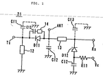
- Fig. 1 is an electrical circuit diagram showing an example of a high-frequency switch 21 according to the present invention.
- the cathode of a diode D11 forming a switching element, is connected to a transmission terminal Tx.
- the cathode of the diode D11 is grounded via a transmission line 12.
- the transmission line 12 functions as a choke element.
- the anode of the diode D11 connects to an antenna terminal ANT.
- a reception terminal Rx is connected via a transmission line 13 to the antenna terminal ANT. Moreover, the cathode of a diode D12 connects to the reception terminal Rx. The anode of the diode D12 connects to the ground via a DC-blocking capacitor C12. A voltage-control terminal Vc connects via a resistor R11 to an intermediate connection point between the diode D12 and the capacitor C12. A control circuit (not shown) is connected to this voltage-control terminal Vc, and switches the transmission lines of the high-frequency switch 21.
- a series circuit comprising a transmission line 14 and a capacitor C13, connects to both ends of the diode D11 (between the anode and the cathode).
- the transmission line 14 and the capacitor C13 are provided in order to achieve good isolation when the diode D11 is in the OFF state.
- distributed constant lines having a characteristic impedance of more than 40 ⁇ or high-frequency inductors, are used as the transmission lines 12 and 13.
- the lengths of the transmission lines 12 and 13 arc set within a range of greater than ⁇ /12 and less than ⁇ /4 (where ⁇ is the wavelength of a desired frequency).
- a distributed constant line or a high-frequency inductor is also used for the transmission line 14.
- floating capacitances Cf1, Cf2, and Cf3 are generated between the terminals Tx, ANT, Rx, and ground, and can function as bypass capacitors for impedance adjustment.
- a transmission signal which has entered the transmission terminal Tx passes through the diode D11, and is sent to the antenna terminal ANT. At this time, most of the transmission signal is not sent to the reception terminal Rx.
- the self-inductance of the diode D12 in the ON state and the capacitance of the capacitor C12 resonate in series at the transmission frequency, whereby the impedance is 0. That is, the transmission lines 12 and 13 operate as a short-stub of length ⁇ /4, and consequently the transmission terminal Tx and the antenna terminal ANT are connected, and the reception terminal Rx is grounded.
- the diodes D11 and D12 switch OFF. Therefore, there is a cut-off between the transmission terminal Tx and the antenna terminal ANT, and in addition, there is a cut-off between the reception terminal Rx and ground. As a result, a received signal which has entered the antenna terminal ANT is sent through the transmission line 13 to the reception terminal Rx, and is mostly not transmitted to the transmission terminal Tx.
- the high-frequency switch 21 is able to switch between the respective transmission paths of transmitted and received signals.
- the high-frequency switch 21 can dispense with the large-capacitance and large-scale DC-blocking capacitor C1 of the conventional high-frequency switch 1. That is, the high-frequency switch 21 requires only the small-capacitance and small-scale capacitor C12, connected between the diode D12 and ground on the reception terminal Rx side.
- the capacitance of the capacitor C12 is, for instance, 10 pF near 1 GHz, and 3 pF near 2 GHz. Consequently, the high-frequency switch 21 can be miniaturized.
- the isolation between the antenna terminal ANT and the reception terminal Rx which is especially important when the transmission terminal Tx and the antenna terminal ANT are connected, can be increased more than in the conventional high-frequency switch. As a result, it is possible to reduce insertion loss between the transmission terminal Tx and the antenna terminal ANT.
- the voltage-control terminal Vc when transmitting (when the diode D12 is in the ON state), the voltage-control terminal Vc is shorted to ground, and when receiving (when the diode D12 is in the OFF state), the voltage-controlled terminal Vc is cut-off from the high-frequency signal by the high impedance of the diode D12, and consequently, it is possible to achieve a large isolation between the control circuit connected to the voltage-control terminal Vc and the high-frequency signal.
- a series circuit comprised of a capacitor C13 and a transmission line 14 may be connected to the diode D11 in parallel.
- the self-inductance of the diode D11 and the inductance of the transmission line 14 form a parallel resonance circuit.
- the high-frequency switch 31 comprises dielectric sheets 45b and 45c respectively provided with distributed constant lines 32a, 32b and the like, dielectric sheets 45d and 45g respectively provided with wide-area ground electrodes 35 and 36, dielectric sheets 45e and 45f respectively provided with distributed constant lines 33a, 34a and 33b, 34b, a dielectric sheet 45a provided with peer-hole pads 50a to 54b, etc.
- the distributed constant lines 33a and 33b are for instance spiral-shaped, and are provided on the left side of the sheets 45e and 45f.
- the extracted portion 42a of the distributed constant line 33a is exposed on the far side near the left side of the sheet 45e, and the extracted portion 42b of the distributed constant line 33b is exposed on the left side of the sheet 45f.
- the distributed constant lines 33a and 33b are electrically connected in series via a peer-hole 58, provided in the sheet 45e, and form the transmission line 12.
- the distributed constant lines 34a and 34b are substantially meander-shaped, and are provided on the right side of the sheets 45e and 45f.
- the extracted portion 43a of the distributed constant line 34a is exposed in the center on the front side of the sheet 45e, and the extracted portion 43b of the distributed constant line 34b is exposed near the right side on the far side of the sheet 45f.
- the distributed constant lines 34a and 34b are electrically connected in series via a peer-hole 59, provided in the sheet 45e, and form the transmission line 13.
- the distributed constant lines 32a and 32b are spiral-shaped, and are provided on the right side of the sheets 45b and 45c.
- the distributed constant lines 32a and 32b are electrically connected in series via a peer-hole 57, provided in the sheet 45b, and form the transmission line 14.
- transmission lines 12 to 14 having fixed impedance characteristics each comprise two layers and comprise distributed constant lines 33a, 33b, 34a, 34b, 32a, and 32b, whereby the length of a transmission line portion on each one layer can be shorter than in the conventional art. Therefore, the size of the sheets 45a-45g can be reduced, obtaining a high-frequency switch 31 which occupies a small area with respect to a printed circuit substrate or the like.
- the ground electrodes 35 and 36 are provided over a wide area on the surfaces of the sheets 45d and 45g.
- the extracted portions 35a and 36a of the ground electrodes 35 and 36 are exposed on the left sides of the sheets 45d and 45g, the extracted portions 35b and 36b are exposed on the right, the extracted portions 35c and 36c are exposed in the center on the far sides of the sheets 45d and 45g, and the extracted portions 35d and 36d are exposed near the right side on the front sides of the sheets 45d and 45g.
- the transmission lines 12 and 13 are provided in parallel between these two ground electrodes 35 and 36.
- extracted electrodes 37, 38, 39, and a relay electrode 40 are provided on the surface of the sheet 45b on which the distributed constant line 32a is provided. Ends of each of the extracted electrodes 37 and 38 are exposed near the left side and right side on the far side of the sheet 45b, and the end of the extracted electrode 39 is exposed near the left side on the front side of the sheet 45b. Then, the distributed constant line 32a is electrically connected to a peer-hole pad 52b, the extracted electrode 37 is electrically connected to peer-hole pads 50a and 52a, the extracted electrode 38 is electrically connected to a peer-hole pad 51a, and the relay electrode 40 is electrically connected to peer-hole pads 53b, 54b, and 51b.
- An extracted electrode 41 is provided on the surface of the sheet 45c on which the distributed constant line 32b is provided. One end of the extracted electrode 41 is exposed in the center of the front side of the sheet 45c. Then, the extracted electrode 41 is electrically connected to the distributed constant line 32b, and in addition, electrically connected via the peer-hole 55 to the peer-hole pad 50b. Furthermore, the peer-hole pad 53a is electrically connected to the ground electrode 35 via the peer-holes 56a and 56b provided in the sheets 45b and 45c.
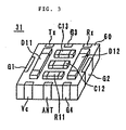
- a transmission terminal Tx, a ground terminal G3, and a reception terminal Rx are provided on the left side, the center, and the right side of the side face portion on the far side of the multilayered body 60.
- a voltage-control terminal Vc, an antenna terminal ANT, and a ground terminal G4 are provided on the left side, the center, and the right side of the side face portion on the front side of the multilayered body 60.
- Ground terminals G1 and G2 are provided on the left and right side face portions of the multilayered body 60.
- the transmission terminal Tx is electrically connected to one end of the transmission line 12 (specifically, to the extracted portion 42a of the distributed constant line 33a), and to the extracted electrode 37.
- the reception terminal Rx is electrically connected to one end of the transmission line 13 (specifically, to the extracted portion 43b of the distributed constant line 34b), and to the extracted electrode 38.
- the antenna terminal ANT is electrically connected to the other end of the transmission line 13 (specifically, to the extracted portion 43a of the distributed constant line 34a), and to the extracted electrode 41.
- the voltage-control terminal Vc is electrically connected to the extracted electrode 39.
- the ground terminal G1 is electrically connected to the other end of the transmission line 12 (specifically, the extracted portion 42b of the distributed constant line 33b), and to the extracted portions 35a and 36a of the ground electrodes 35 and 36.
- the ground terminals G2, G3, and G4 are electrically connected respectively to the extracted portions 35b, 36b, 35c, 36c, 35d, and 36d of the ground electrodes 35 and 36.
- the cathode electrode and anode electrode of the diode D11 are soldered to the pads 50a and 50b on the multilayered body 60
- the cathode electrode and anode electrode of the diode D12 are soldered to the pads 51a and 51b
- the terminal electrodes of the capacitor C13 are soldered to the pads 52a and 52b
- the terminal electrodes of the capacitor C12 are soldered to the pads 53a and 53b
- the terminal electrodes of the resistor R11 are soldered to the pads 54a and 54b.
- This multilayered high-frequency switch 31 does not require a large-capacitance DC-blocking capacitor C1, as in the conventional high-frequency switch 1 shown in Fig. 6 , to be incorporated in or mounted on the multilayered body 60, and consequently even though the transmission lines 12 to 14 each comprise two layers, the number of layers in the multilayered body 60 can be reduced.
- the size of the sheets 45a-45g can be reduced, reducing the area occupied by the high-frequency switch 31 on a printed circuit substrate or the like.
- a resistor Ra an external component
- the high-frequency switch 31 since one end of the transmission line 12 connects to the ground terminal G1, interconnection is simple, thereby enabling the number of layers in the multilayered body 60 to be reduced, and leading to a consequent improvement in transmission loss by eliminating unnecessary coupling.
- FIG. 4 and Fig. 5 Another example of a multilayered high-frequency switch having the electrical circuit shown in Fig. 1 will be explained referring to Fig. 4 and Fig. 5 .
- the high-frequency switch 61 of this second embodiment contains a DC-blocking capacitor C12 within its multilayered body.
- Figs. 4 and 5 the same parts as those in Figs. 2 and 3 are represented by the same reference numerals, and explanation thereof is omitted.
- the high-frequency switch 61 comprises a dielectric sheet 45j; comprising a distributed constant line 62 and a capacitor electrode 70, dielectric sheets 45d and 45g comprising wide-area ground electrodes 35 and 36, a dielectric sheet 45k comprising distributed constant lines 63 and 64, a dielectric sheet 45i; comprising extracted electrodes 37 and 38 and the like, a dielectric sheet 45h comprising peer-hole pads 50a and 50b and the like, etc.
- the distributed constant line 62 is for instance meander-shaped, and forms a transmission line 14. One end of the distributed constant line 62 is electrically connected to the extracted electrode 41, and the other end is electrically connected to the peer-hole pad 52b via a peer-hole 67, provided in the sheet 45i.
- the distributed constant lines 63 and 64 are substantially meander-shaped, and respectively form transmission lines 12 and 13. One extracted portion 63a of the distributed constant line 63 is exposed near the left side on the far side of the sheet 45k, and the other extracted portion 63b is exposed the left side of the sheet 45k. One extracted portion 64a of the distributed constant line 64 is exposed in the center of the front side of the sheet 45k, and the other extracted portion 64b is exposed near the right side on the far side of the sheet 45k. In this way, since the transmission lines 12 to 14 each comprise one-layer distributed constant lines 63, 64, and 62 respectively, the number of layers of the multilayered body 80 (explained later) can be further reduced.
- the capacitor electrode 70 is formed on the sheet 45j on the side thereof away from the ground electrode 35, and together with the ground electrode 35 forms a capacitor C12.
- the capacitor electrode 70 electrically connects via a peer-hole 66 to the relay electrode 65 provided on the sheet 45i.
- the relay electrode 65 is electrically connected to the peer-hole pads 51b and 54b.
- the multilayered body 80 As shown in Fig. 5 is obtained.
- a transmission terminal Tx, a ground terminal G3, and a reception terminal Rx are provided on the side face portion at the far side of the multilayered body 80.
- a voltage-control terminal Vc, an antenna terminal ANT, and a ground terminal G4 are provided on the side face portion at the front side of the multilayered body 80.
- Ground terminals G1 and G2 are provided on the left and right side face portions of the multilayered body 80.
- the transmission terminal Tx is electrically connected to the extracted portion 63a of the distributed constant line 63, and to the extracted electrode 37.
- the reception terminal Rx is electrically connected to the extracted portion 64a of the distributed constant line 64, and to the extracted electrode 38.
- the antenna terminal ANT is electrically connected to the extracted portion 64a of the distributed constant line 64, and to the extracted electrode 41.
- the voltage-control terminal Vc is electrically connected to the extracted electrode 39.
- the ground terminal G1 is electrically connected to the extracted portion 63b of the distributed constant line 63, and to the extracted portions 35a and 36a of the ground electrodes 35 and 36.
- the ground terminals G2, G3, and G4 are electrically connected to the extracted portions 35b, 36b, 35c, 36c, 35d, and 36d of the ground electrodes 35 and 36 respectively.
- the cathode electrode and anode electrode of the diode D11 are soldered to the pads 50a and 50b on the multilayered body 80
- the cathode electrode and anode electrode of the diode D12 are soldered to the pads 51a and 51b
- the terminal electrodes of the capacitor C13 are soldered to the pads 52a and 52b
- the terminal electrodes of the resistor R11 are soldered to the pads 54a and 54b.
- the capacitor C12 is contained in the multilayered body 80, the length of the interconnection from the capacitor C12 to ground is shorter than when the capacitor C12 is mounted on the multilayered body as an external component. Therefore, there is less residual impedance, improving the DC bias-blocking effect. Moreover, the value of the capacitor C12 can be minutely adjusted by changing the size of the capacitor electrode 70, a greater isolation can be achieved between the antenna terminal ANT and the reception terminal Rx when the transmission terminal Tx and the antenna terminal ANT are connected than in a conventional high-frequency switch, and there is a reduction in insertion loss between the transmission terminal Tx and the antenna terminal ANT.
- the high-frequency switch according to the present invention is not restricted to the embodiments described above, and various modifications can be made thereto within the scope of its main features.
- the series circuit comprising the transmission line and the capacitor may be connected to both ends (between the anode and the cathode) of the diode D12.
- capacitors may be connected in parallel to both ends (between the anode and the cathode) of the diodes D11 and D12, in parallel with the series circuit comprising the transmission line and the capacitor, improving the isolation when the diodes D11 and D12 are OFF.
- resistances greater than 10K ⁇
Landscapes
- Engineering & Computer Science (AREA)
- Computer Networks & Wireless Communication (AREA)
- Signal Processing (AREA)
- Transceivers (AREA)
- Waveguide Switches, Polarizers, And Phase Shifters (AREA)
- Electronic Switches (AREA)
Claims (3)
- Ein Hochfrequenzschalter (21; 31; 61), der folgende Merkmale aufweist:einen mehrschichtigen Körper;einen Sendeanschluss (Tx), einen Antennenanschluss (ANT), einen Empfangsanschluss (Rx) und einen Spannungssteueranschluss (Vc), die auf einer äußeren Oberfläche des mehrschichtigen Körpers vorgesehen sind;eine erste Diode (D11), deren Kathode elektrisch mit dem Sendeanschluss (Tx) verbunden ist, wobei die Anode elektrisch mit dem Antennenanschluss (ANT) verbunden ist;eine erste Übertragungsleitung (13), die elektrisch zwischen den Antennenanschluss (ANT) und den Empfangsanschluss (Rx) geschaltet ist;eine zweite Diode (D12), deren Kathode elektrisch mit dem Empfangsanschluss (Rx) verbunden ist, wobei die Anode elektrisch mit dem Spannungssteueranschluss (Vc) verbunden ist;einen Hochfrequenzinduktor (12), dessen eines Ende elektrisch mit dem Sendeanschluss (Tx) verbunden ist, wobei das andere Ende direkt mit Masse verbunden ist; undeinen Gleichsignalblockierungskondensator (C12), der elektrisch zwischen den Spannungssteueranschluss (Vc) und Masse geschaltet ist und in Serie zu der zweiten Diode (D12) geschaltet ist;wobei ein Ende des Hochfrequenzinduktors (12) und die Kathode der ersten Diode (D11) direkt miteinander verbunden sind;wobei ein festgelegtes Potential an den Spannungssteueranschluss (Vc) angelegt ist, so dass die erste Diode (D11) und die zweite Diode (D 12) gleichzeitig an- oder ausgeschaltet werden; undwobei die erste und die zweite Diode (D11, D 12) an der äußeren Oberfläche des mehrschichtigen Körpers befestigt sind;dadurch gekennzeichnet, dassder Hochfrequenzschalter (21; 31; 61) einen einzelnen Gleichsignalblockierungskondensator (C 12) aufweist;der Gleichsignalblockierungskondensator (C12) auf dem mehrschichtigen Körper oder in dem mehrschichtigen Körper gebildet ist;in dem AN-Zustand die Eigeninduktivität der zweiten Diode (D12) und die Kapazität des Gleichsignalblockierungskondensators (C12) bei einer Übertragungsfrequenz in Serie in Resonanz sind, undder Hochfrequenzschalter (21; 31; 61) zur Impedanzanpassung schwebende Kapazitäten zwischen dem Sendeanschluss (Tx) und Masse, dem Antennenanschluss (ANT) und Masse und dem Empfangsanschluss (Rx) und Masse aufweist.
- Der Hochfrequenzschalter gemäß Anspruch 1, bei dem:der mehrschichtige Körper eine Mehrzahl laminierter dielektrischer Schichten (45a-45k), an denen sich Elektroden befinden, aufweist, wobei die Elektroden die erste und die zweite Übertragungsleitung (13, 14), eine Kondensatorelektrode des Gleichsignalblockierungskondensators und eine Masseelektrode bilden; unddie erste und die zweite Diode (D11, D12), die an der äußeren Oberfläche des mehrschichtigen Körpers befestigt sind, mit den Elektroden verbunden sind.
- Der Hochfrequenzschalter gemäß Anspruch 1, bei dem:der mehrschichtige Körper eine Mehrzahl laminierter dielektrischer Schichten (45a-45k), an denen sich Elektroden befinden, aufweist, wobei die Elektroden die erste Übertragungsleitung (13) und den Hochfrequenzinduktor (12) bilden; unddie erste und die zweite Diode (D11, D12), die an der äußeren Oberfläche des mehrschichtigen Körpers befestigt sind, mit den Elektroden verbunden sind.
Applications Claiming Priority (3)
| Application Number | Priority Date | Filing Date | Title |
|---|---|---|---|
| JP01866299A JP3675210B2 (ja) | 1999-01-27 | 1999-01-27 | 高周波スイッチ |
| JP1866299 | 1999-01-27 | ||
| EP00100027A EP1024605A3 (de) | 1999-01-27 | 2000-01-04 | Hochfrequenzschalter |
Related Parent Applications (2)
| Application Number | Title | Priority Date | Filing Date |
|---|---|---|---|
| EP00100027A Division EP1024605A3 (de) | 1999-01-27 | 2000-01-04 | Hochfrequenzschalter |
| EP00100027.2 Division | 2000-01-04 |
Publications (3)
| Publication Number | Publication Date |
|---|---|
| EP1583253A2 EP1583253A2 (de) | 2005-10-05 |
| EP1583253A3 EP1583253A3 (de) | 2005-10-26 |
| EP1583253B1 true EP1583253B1 (de) | 2010-07-14 |
Family
ID=11977836
Family Applications (2)
| Application Number | Title | Priority Date | Filing Date |
|---|---|---|---|
| EP05014478A Expired - Lifetime EP1583253B1 (de) | 1999-01-27 | 2000-01-04 | Hochfrequenzschalter |
| EP00100027A Withdrawn EP1024605A3 (de) | 1999-01-27 | 2000-01-04 | Hochfrequenzschalter |
Family Applications After (1)
| Application Number | Title | Priority Date | Filing Date |
|---|---|---|---|
| EP00100027A Withdrawn EP1024605A3 (de) | 1999-01-27 | 2000-01-04 | Hochfrequenzschalter |
Country Status (6)
| Country | Link |
|---|---|
| US (3) | US6633206B1 (de) |
| EP (2) | EP1583253B1 (de) |
| JP (1) | JP3675210B2 (de) |
| KR (1) | KR100324720B1 (de) |
| DE (1) | DE60044687D1 (de) |
| SG (1) | SG92665A1 (de) |
Families Citing this family (32)
| Publication number | Priority date | Publication date | Assignee | Title |
|---|---|---|---|---|
| JP3675210B2 (ja) * | 1999-01-27 | 2005-07-27 | 株式会社村田製作所 | 高周波スイッチ |
| JP3813083B2 (ja) * | 2001-12-05 | 2006-08-23 | ローム株式会社 | 送受信装置 |
| US7221922B2 (en) * | 2003-02-14 | 2007-05-22 | Hitachi Metals, Ltd. | Switch circuit and composite high frequency elements |
| US6998933B1 (en) * | 2004-08-03 | 2006-02-14 | Agilent Technologies, Inc. | Millimeter wave switch |
| US8031129B2 (en) | 2004-08-18 | 2011-10-04 | Ruckus Wireless, Inc. | Dual band dual polarization antenna array |
| US7880683B2 (en) | 2004-08-18 | 2011-02-01 | Ruckus Wireless, Inc. | Antennas with polarization diversity |
| US7362280B2 (en) | 2004-08-18 | 2008-04-22 | Ruckus Wireless, Inc. | System and method for a minimized antenna apparatus with selectable elements |
| US7292198B2 (en) | 2004-08-18 | 2007-11-06 | Ruckus Wireless, Inc. | System and method for an omnidirectional planar antenna apparatus with selectable elements |
| US7696946B2 (en) | 2004-08-18 | 2010-04-13 | Ruckus Wireless, Inc. | Reducing stray capacitance in antenna element switching |
| US7498996B2 (en) | 2004-08-18 | 2009-03-03 | Ruckus Wireless, Inc. | Antennas with polarization diversity |
| US7965252B2 (en) | 2004-08-18 | 2011-06-21 | Ruckus Wireless, Inc. | Dual polarization antenna array with increased wireless coverage |
| US7652632B2 (en) | 2004-08-18 | 2010-01-26 | Ruckus Wireless, Inc. | Multiband omnidirectional planar antenna apparatus with selectable elements |
| US7193562B2 (en) | 2004-11-22 | 2007-03-20 | Ruckus Wireless, Inc. | Circuit board having a peripheral antenna apparatus with selectable antenna elements |
| KR100794473B1 (ko) * | 2004-09-30 | 2008-01-17 | 가부시키가이샤 무라타 세이사쿠쇼 | 고주파 스위치 및 그 제조방법 |
| US7400862B2 (en) * | 2004-10-25 | 2008-07-15 | Skyworks Solutions, Inc. | Transmit-receive switch architecture providing pre-transmit isolation |
| CN1934750B (zh) | 2004-11-22 | 2012-07-18 | 鲁库斯无线公司 | 包括具有可选择天线元件的外围天线装置的电路板 |
| US7358912B1 (en) | 2005-06-24 | 2008-04-15 | Ruckus Wireless, Inc. | Coverage antenna apparatus with selectable horizontal and vertical polarization elements |
| US7646343B2 (en) | 2005-06-24 | 2010-01-12 | Ruckus Wireless, Inc. | Multiple-input multiple-output wireless antennas |
| US7893882B2 (en) | 2007-01-08 | 2011-02-22 | Ruckus Wireless, Inc. | Pattern shaping of RF emission patterns |
| CN101128985A (zh) | 2005-08-26 | 2008-02-20 | 株式会社村田制作所 | 高频开关 |
| US7639106B2 (en) * | 2006-04-28 | 2009-12-29 | Ruckus Wireless, Inc. | PIN diode network for multiband RF coupling |
| EP2051394B1 (de) * | 2006-08-09 | 2017-05-10 | Hitachi Metals, Ltd. | Hochfrequenzkomponente und hochfrequenzschaltung zur verwendung darin |
| US8217843B2 (en) | 2009-03-13 | 2012-07-10 | Ruckus Wireless, Inc. | Adjustment of radiation patterns utilizing a position sensor |
| US8698675B2 (en) | 2009-05-12 | 2014-04-15 | Ruckus Wireless, Inc. | Mountable antenna elements for dual band antenna |
| US9407012B2 (en) | 2010-09-21 | 2016-08-02 | Ruckus Wireless, Inc. | Antenna with dual polarization and mountable antenna elements |
| US8756668B2 (en) | 2012-02-09 | 2014-06-17 | Ruckus Wireless, Inc. | Dynamic PSK for hotspots |
| US9634403B2 (en) | 2012-02-14 | 2017-04-25 | Ruckus Wireless, Inc. | Radio frequency emission pattern shaping |
| US10186750B2 (en) | 2012-02-14 | 2019-01-22 | Arris Enterprises Llc | Radio frequency antenna array with spacing element |
| US9092610B2 (en) | 2012-04-04 | 2015-07-28 | Ruckus Wireless, Inc. | Key assignment for a brand |
| US9570799B2 (en) | 2012-09-07 | 2017-02-14 | Ruckus Wireless, Inc. | Multiband monopole antenna apparatus with ground plane aperture |
| EP2728759B1 (de) * | 2012-10-30 | 2016-08-24 | Panasonic Corporation | Antennenanpassungsschaltung für drahtlose Kommunikationsvorrichtung |
| EP2974045A4 (de) | 2013-03-15 | 2016-11-09 | Ruckus Wireless Inc | Niedrigbandreflektor für eine gerichtete doppelbandantenne |
Family Cites Families (19)
| Publication number | Priority date | Publication date | Assignee | Title |
|---|---|---|---|---|
| JP2874496B2 (ja) * | 1992-12-26 | 1999-03-24 | 株式会社村田製作所 | 高周波スイッチ |
| JP3291913B2 (ja) * | 1994-05-17 | 2002-06-17 | 株式会社村田製作所 | 高周波スイッチ |
| JP3031178B2 (ja) * | 1994-09-28 | 2000-04-10 | 株式会社村田製作所 | 複合高周波部品 |
| WO1996013101A1 (en) * | 1994-10-24 | 1996-05-02 | Motorola Inc. | Multi-function radio frequency circuit |
| JP3235380B2 (ja) | 1994-11-30 | 2001-12-04 | 株式会社村田製作所 | 高周波スイッチ |
| JPH08162803A (ja) | 1994-12-07 | 1996-06-21 | Murata Mfg Co Ltd | Rfスイッチ |
| JP3299065B2 (ja) * | 1995-01-30 | 2002-07-08 | 株式会社村田製作所 | 高周波複合スイッチ |
| US5625894A (en) * | 1995-03-21 | 1997-04-29 | Industrial Technology Research Institute | Switch filter having selectively interconnected filter stages and ports |
| JP3139352B2 (ja) | 1995-09-01 | 2001-02-26 | 株式会社村田製作所 | 高周波スイッチ |
| DE19610760A1 (de) * | 1996-03-19 | 1997-09-25 | Telefunken Microelectron | Sende-Empfangs-Umschalter mit Halbleitern |
| JPH09260901A (ja) * | 1996-03-27 | 1997-10-03 | Hitachi Metals Ltd | スイッチ回路 |
| JPH1056301A (ja) * | 1996-08-08 | 1998-02-24 | Murata Mfg Co Ltd | 高周波スイッチ |
| JPH10145270A (ja) | 1996-11-14 | 1998-05-29 | Murata Mfg Co Ltd | 高周波デバイス |
| JP3887805B2 (ja) * | 1997-03-28 | 2007-02-28 | 日立金属株式会社 | ダイオードスイッチ |
| JP3780394B2 (ja) | 1997-06-25 | 2006-05-31 | 株式会社村田製作所 | 高周波伝送線路及び高周波伝送線路を有した電子部品 |
| JPH11168303A (ja) | 1997-12-05 | 1999-06-22 | Hitachi Metals Ltd | 高周波スイッチモジュール |
| JP2983016B2 (ja) | 1997-12-03 | 1999-11-29 | 日立金属株式会社 | マルチバンド用高周波スイッチモジュール |
| US6289204B1 (en) * | 1998-07-09 | 2001-09-11 | Motorola, Inc. | Integration of a receiver front-end in multilayer ceramic integrated circuit technology |
| JP3675210B2 (ja) * | 1999-01-27 | 2005-07-27 | 株式会社村田製作所 | 高周波スイッチ |
-
1999
- 1999-01-27 JP JP01866299A patent/JP3675210B2/ja not_active Expired - Fee Related
-
2000
- 2000-01-04 DE DE60044687T patent/DE60044687D1/de not_active Expired - Lifetime
- 2000-01-04 EP EP05014478A patent/EP1583253B1/de not_active Expired - Lifetime
- 2000-01-04 EP EP00100027A patent/EP1024605A3/de not_active Withdrawn
- 2000-01-06 SG SG200000079A patent/SG92665A1/en unknown
- 2000-01-24 KR KR1020000003152A patent/KR100324720B1/ko not_active Expired - Fee Related
- 2000-01-27 US US09/492,927 patent/US6633206B1/en not_active Expired - Lifetime
-
2003
- 2003-04-28 US US10/423,967 patent/US6897738B2/en not_active Expired - Lifetime
-
2005
- 2005-01-12 US US11/034,278 patent/US7391284B2/en not_active Expired - Fee Related
Also Published As
| Publication number | Publication date |
|---|---|
| US20030206079A1 (en) | 2003-11-06 |
| US6897738B2 (en) | 2005-05-24 |
| EP1024605A2 (de) | 2000-08-02 |
| KR20000053587A (ko) | 2000-08-25 |
| EP1583253A2 (de) | 2005-10-05 |
| US20050122184A1 (en) | 2005-06-09 |
| EP1583253A3 (de) | 2005-10-26 |
| US7391284B2 (en) | 2008-06-24 |
| JP3675210B2 (ja) | 2005-07-27 |
| SG92665A1 (en) | 2002-11-19 |
| EP1024605A3 (de) | 2003-12-03 |
| US6633206B1 (en) | 2003-10-14 |
| DE60044687D1 (de) | 2010-08-26 |
| KR100324720B1 (ko) | 2002-02-28 |
| JP2000223901A (ja) | 2000-08-11 |
Similar Documents
| Publication | Publication Date | Title |
|---|---|---|
| EP1583253A2 (de) | Hochfrequenzschalter | |
| US6768898B2 (en) | Composite high frequency component and mobile communication apparatus including the same | |
| US7200365B2 (en) | Composite high frequency component and mobile communication device including the same | |
| JP3031178B2 (ja) | 複合高周波部品 | |
| EP0928038B1 (de) | Zweifrequenzschalter, anordnung mit gemeinsamer zweifrequenzantenne und mobile zweifrequenz-funkübertragungsausrüstung damit | |
| US6985712B2 (en) | RF device and communication apparatus using the same | |
| US7398103B2 (en) | High-frequency module and mobile communication apparatus using the same | |
| US6928298B2 (en) | Mobile communication device and high-frequency composite unit used in the same | |
| JPH09200077A (ja) | 複合高周波部品 | |
| EP1126624B1 (de) | Hochfrequenzscalter | |
| US5999065A (en) | Composite high-frequency component | |
| WO2004073193A1 (ja) | スイッチ回路及び複合高周波部品 | |
| EP0929151B1 (de) | Filter | |
| JPH10276117A (ja) | 複合スイッチ回路部品 | |
| JP3832484B2 (ja) | 高周波スイッチ | |
| JP2004328136A (ja) | ローパスフィルタ及びそれを用いた高周波スイッチ | |
| JPH10276003A (ja) | ダイオードスイッチ | |
| JP4193873B2 (ja) | 高周波スイッチ | |
| JP2004312498A (ja) | ローパスフィルタ及びそれを用いた高周波スイッチ |
Legal Events
| Date | Code | Title | Description |
|---|---|---|---|
| PUAI | Public reference made under article 153(3) epc to a published international application that has entered the european phase |
Free format text: ORIGINAL CODE: 0009012 |
|
| PUAL | Search report despatched |
Free format text: ORIGINAL CODE: 0009013 |
|
| 17P | Request for examination filed |
Effective date: 20050704 |
|
| AC | Divisional application: reference to earlier application |
Ref document number: 1024605 Country of ref document: EP Kind code of ref document: P |
|
| AK | Designated contracting states |
Kind code of ref document: A2 Designated state(s): AT BE CH CY DE DK ES FI FR GB GR IE IT LI LU MC NL PT SE |
|
| AX | Request for extension of the european patent |
Extension state: AL LT LV MK RO SI |
|
| AK | Designated contracting states |
Kind code of ref document: A3 Designated state(s): AT BE CH CY DE DK ES FI FR GB GR IE IT LI LU MC NL PT SE |
|
| AX | Request for extension of the european patent |
Extension state: AL LT LV MK RO SI |
|
| AKX | Designation fees paid |
Designated state(s): DE FR GB |
|
| RAP1 | Party data changed (applicant data changed or rights of an application transferred) |
Owner name: MURATA MANUFACTURING CO., LTD. |
|
| GRAP | Despatch of communication of intention to grant a patent |
Free format text: ORIGINAL CODE: EPIDOSNIGR1 |
|
| RIN1 | Information on inventor provided before grant (corrected) |
Inventor name: KATO, MITSUHIDE |
|
| GRAS | Grant fee paid |
Free format text: ORIGINAL CODE: EPIDOSNIGR3 |
|
| GRAA | (expected) grant |
Free format text: ORIGINAL CODE: 0009210 |
|
| AC | Divisional application: reference to earlier application |
Ref document number: 1024605 Country of ref document: EP Kind code of ref document: P |
|
| AK | Designated contracting states |
Kind code of ref document: B1 Designated state(s): DE FR GB |
|
| REG | Reference to a national code |
Ref country code: GB Ref legal event code: FG4D |
|
| REF | Corresponds to: |
Ref document number: 60044687 Country of ref document: DE Date of ref document: 20100826 Kind code of ref document: P |
|
| PLBE | No opposition filed within time limit |
Free format text: ORIGINAL CODE: 0009261 |
|
| STAA | Information on the status of an ep patent application or granted ep patent |
Free format text: STATUS: NO OPPOSITION FILED WITHIN TIME LIMIT |
|
| PGFP | Annual fee paid to national office [announced via postgrant information from national office to epo] |
Ref country code: FR Payment date: 20110209 Year of fee payment: 12 |
|
| 26N | No opposition filed |
Effective date: 20110415 |
|
| REG | Reference to a national code |
Ref country code: DE Ref legal event code: R097 Ref document number: 60044687 Country of ref document: DE Effective date: 20110415 |
|
| PGFP | Annual fee paid to national office [announced via postgrant information from national office to epo] |
Ref country code: GB Payment date: 20110121 Year of fee payment: 12 |
|
| GBPC | Gb: european patent ceased through non-payment of renewal fee |
Effective date: 20120104 |
|
| REG | Reference to a national code |
Ref country code: FR Ref legal event code: ST Effective date: 20120928 |
|
| PG25 | Lapsed in a contracting state [announced via postgrant information from national office to epo] |
Ref country code: GB Free format text: LAPSE BECAUSE OF NON-PAYMENT OF DUE FEES Effective date: 20120104 |
|
| PG25 | Lapsed in a contracting state [announced via postgrant information from national office to epo] |
Ref country code: FR Free format text: LAPSE BECAUSE OF NON-PAYMENT OF DUE FEES Effective date: 20120131 |
|
| PGFP | Annual fee paid to national office [announced via postgrant information from national office to epo] |
Ref country code: DE Payment date: 20170120 Year of fee payment: 18 |
|
| REG | Reference to a national code |
Ref country code: DE Ref legal event code: R119 Ref document number: 60044687 Country of ref document: DE |
|
| PG25 | Lapsed in a contracting state [announced via postgrant information from national office to epo] |
Ref country code: DE Free format text: LAPSE BECAUSE OF NON-PAYMENT OF DUE FEES Effective date: 20180801 |