EP1583160A2 - Microelektronischer Aufbau mit optischem Fenster auf der Chip-Unterseite und dessen Herstellung - Google Patents
Microelektronischer Aufbau mit optischem Fenster auf der Chip-Unterseite und dessen Herstellung Download PDFInfo
- Publication number
- EP1583160A2 EP1583160A2 EP05075731A EP05075731A EP1583160A2 EP 1583160 A2 EP1583160 A2 EP 1583160A2 EP 05075731 A EP05075731 A EP 05075731A EP 05075731 A EP05075731 A EP 05075731A EP 1583160 A2 EP1583160 A2 EP 1583160A2
- Authority
- EP
- European Patent Office
- Prior art keywords
- substrate
- encapsulant
- integrated circuit
- gap
- central region
- Prior art date
- Legal status (The legal status is an assumption and is not a legal conclusion. Google has not performed a legal analysis and makes no representation as to the accuracy of the status listed.)
- Withdrawn
Links
Images

Classifications
-
- H—ELECTRICITY
- H10—SEMICONDUCTOR DEVICES; ELECTRIC SOLID-STATE DEVICES NOT OTHERWISE PROVIDED FOR
- H10W—GENERIC PACKAGES, INTERCONNECTIONS, CONNECTORS OR OTHER CONSTRUCTIONAL DETAILS OF DEVICES COVERED BY CLASS H10
- H10W74/00—Encapsulations, e.g. protective coatings
- H10W74/10—Encapsulations, e.g. protective coatings characterised by their shape or disposition
- H10W74/131—Encapsulations, e.g. protective coatings characterised by their shape or disposition the semiconductor body being only partially enclosed
- H10W74/141—Encapsulations, e.g. protective coatings characterised by their shape or disposition the semiconductor body being only partially enclosed the encapsulations being on at least the sidewalls of the semiconductor body
-
- H—ELECTRICITY
- H10—SEMICONDUCTOR DEVICES; ELECTRIC SOLID-STATE DEVICES NOT OTHERWISE PROVIDED FOR
- H10F—INORGANIC SEMICONDUCTOR DEVICES SENSITIVE TO INFRARED RADIATION, LIGHT, ELECTROMAGNETIC RADIATION OF SHORTER WAVELENGTH OR CORPUSCULAR RADIATION
- H10F39/00—Integrated devices, or assemblies of multiple devices, comprising at least one element covered by group H10F30/00, e.g. radiation detectors comprising photodiode arrays
- H10F39/80—Constructional details of image sensors
- H10F39/804—Containers or encapsulations
-
- H—ELECTRICITY
- H10—SEMICONDUCTOR DEVICES; ELECTRIC SOLID-STATE DEVICES NOT OTHERWISE PROVIDED FOR
- H10F—INORGANIC SEMICONDUCTOR DEVICES SENSITIVE TO INFRARED RADIATION, LIGHT, ELECTROMAGNETIC RADIATION OF SHORTER WAVELENGTH OR CORPUSCULAR RADIATION
- H10F77/00—Constructional details of devices covered by this subclass
- H10F77/50—Encapsulations or containers
-
- H—ELECTRICITY
- H10—SEMICONDUCTOR DEVICES; ELECTRIC SOLID-STATE DEVICES NOT OTHERWISE PROVIDED FOR
- H10W—GENERIC PACKAGES, INTERCONNECTIONS, CONNECTORS OR OTHER CONSTRUCTIONAL DETAILS OF DEVICES COVERED BY CLASS H10
- H10W74/00—Encapsulations, e.g. protective coatings
- H10W74/10—Encapsulations, e.g. protective coatings characterised by their shape or disposition
- H10W74/111—Encapsulations, e.g. protective coatings characterised by their shape or disposition the semiconductor body being completely enclosed
- H10W74/124—Encapsulations, e.g. protective coatings characterised by their shape or disposition the semiconductor body being completely enclosed the encapsulations having cavities other than that occupied by chips
-
- H—ELECTRICITY
- H10—SEMICONDUCTOR DEVICES; ELECTRIC SOLID-STATE DEVICES NOT OTHERWISE PROVIDED FOR
- H10W—GENERIC PACKAGES, INTERCONNECTIONS, CONNECTORS OR OTHER CONSTRUCTIONAL DETAILS OF DEVICES COVERED BY CLASS H10
- H10W74/00—Encapsulations, e.g. protective coatings
- H10W74/40—Encapsulations, e.g. protective coatings characterised by their materials
- H10W74/47—Encapsulations, e.g. protective coatings characterised by their materials comprising organic materials, e.g. plastics or resins
-
- H—ELECTRICITY
- H10—SEMICONDUCTOR DEVICES; ELECTRIC SOLID-STATE DEVICES NOT OTHERWISE PROVIDED FOR
- H10H—INORGANIC LIGHT-EMITTING SEMICONDUCTOR DEVICES HAVING POTENTIAL BARRIERS
- H10H20/00—Individual inorganic light-emitting semiconductor devices having potential barriers, e.g. light-emitting diodes [LED]
- H10H20/80—Constructional details
- H10H20/85—Packages
- H10H20/852—Encapsulations
- H10H20/853—Encapsulations characterised by their shape
-
- H—ELECTRICITY
- H10—SEMICONDUCTOR DEVICES; ELECTRIC SOLID-STATE DEVICES NOT OTHERWISE PROVIDED FOR
- H10W—GENERIC PACKAGES, INTERCONNECTIONS, CONNECTORS OR OTHER CONSTRUCTIONAL DETAILS OF DEVICES COVERED BY CLASS H10
- H10W72/00—Interconnections or connectors in packages
- H10W72/90—Bond pads, in general
-
- H—ELECTRICITY
- H10—SEMICONDUCTOR DEVICES; ELECTRIC SOLID-STATE DEVICES NOT OTHERWISE PROVIDED FOR
- H10W—GENERIC PACKAGES, INTERCONNECTIONS, CONNECTORS OR OTHER CONSTRUCTIONAL DETAILS OF DEVICES COVERED BY CLASS H10
- H10W72/00—Interconnections or connectors in packages
- H10W72/90—Bond pads, in general
- H10W72/941—Dispositions of bond pads
- H10W72/9415—Dispositions of bond pads relative to the surface, e.g. recessed, protruding
-
- H—ELECTRICITY
- H10—SEMICONDUCTOR DEVICES; ELECTRIC SOLID-STATE DEVICES NOT OTHERWISE PROVIDED FOR
- H10W—GENERIC PACKAGES, INTERCONNECTIONS, CONNECTORS OR OTHER CONSTRUCTIONAL DETAILS OF DEVICES COVERED BY CLASS H10
- H10W72/00—Interconnections or connectors in packages
- H10W72/90—Bond pads, in general
- H10W72/941—Dispositions of bond pads
- H10W72/944—Dispositions of multiple bond pads
- H10W72/9445—Top-view layouts, e.g. mirror arrays
-
- H—ELECTRICITY
- H10—SEMICONDUCTOR DEVICES; ELECTRIC SOLID-STATE DEVICES NOT OTHERWISE PROVIDED FOR
- H10W—GENERIC PACKAGES, INTERCONNECTIONS, CONNECTORS OR OTHER CONSTRUCTIONAL DETAILS OF DEVICES COVERED BY CLASS H10
- H10W90/00—Package configurations
- H10W90/701—Package configurations characterised by the relative positions of pads or connectors relative to package parts
- H10W90/721—Package configurations characterised by the relative positions of pads or connectors relative to package parts of bump connectors
- H10W90/724—Package configurations characterised by the relative positions of pads or connectors relative to package parts of bump connectors between a chip and a stacked insulating package substrate, interposer or RDL
Definitions
- This invention relates to a microelectronic assembly that includes an integrated circuit die attached to a substrate by solder bump interconnections. More particularly, this invention relates to such assembly that includes an overmolded polymeric encapsulant that extends within a gap between the integrated circuit die and the substrate to protect the solder bump interconnections and further that defines an optical window to allow the integrated circuit device to receive and emit optical signals through the substrate.
- a typical flip chip microelectronic assembly comprises an integrated circuit die, also commonly referred to as a chip, mounted on a substrate, such as a printed circuit board, by solder bump interconnections that physically attach the chip to the substrate and also form electrical connections for conducting electrical signals to and from the chip for processing.
- solder bumps are affixed to bond pads disposed on the active face of the chip.
- the chip is arranged on the substrate, and the arrangement is heated and cooled to reflow the solder and thereby form the interconnections.
- the chip is spaced apart from the substrate by a gap.
- the space about the solder bump interconnections within the gap is typically filled with a polymeric encapsulant.
- the encapsulant protects the solder bump interconnections from corrosion; and also reinforces the interconnections to withstand vibration and other mechanical forces to which the assembly is subjected during use.
- the encapsulant is composed of a polymeric matrix and contains an addition, typically between about 75% and 90% per cent by weight, of particulate silica or other inorganic filler to reduce the CTE to within the desired range.
- the high filler content produces an encapsulant that is opaque.
- a digital camera comprises a die having an array of light sensors that receive and process light to produce an image.
- Other known dies include optical emitter or detector for sending or receiving optical signals for processing.
- the optical element is formed as on the active face of the die and receives or emits signals generally perpendicular to the face.
- the optical signal is received through or emitted toward the substrate.
- Opaque encapsulant within the gap blocks the optical signal and thus interferes with useful operation of the assembly.
- a microelectronic assembly comprises an integrated circuit die mounted on a substrate by a plurality of bump interconnections.
- the die includes an active face having a central region surrounded by a perimeter region, and is arranged relative to the substrate such that the active face faces the substrate and is spaced apart by a gap.
- the bump interconnections are bonded to the perimeter region of the die and to the substrate, to thereby attach the die to the substrate.
- the assembly also includes a polymeric encapsulant about the die on the substrate and extending into the gap to encapsulate the interconnections.
- the encapsulant defines an optical window within the gap underlying the central region. It is an advantage of this invention that the window allows optical access to the active face of the die, including the optical sensors thereon.
- the assembly may be formed using an encapsulant having a desired CTE that is adjusted for protecting the bump interconnections from thermally induced stress.
- a method for forming a microelectronic assembly having an overmolded polymeric encapsulant that defines an underchip optical window.
- the method comprises attaching an integrated circuit device to a substrate by a plurality of bump interconnections, such that the active face of the die faces the substrate spaced apart by a gap.
- the bump interconnections are bonded to the die at a perimeter region surrounding a central region.
- the method further comprises molding or otherwise disposing a polymeric encapsulant about said integrated circuit device on said substrate such that the polymeric encapsulant extends within the gap to encapsulate the bump interconnections, but not within the central region.
- this is accomplished by forming a molding cavity about the die on the substrate, injecting a polymeric material into the cavity at a first pressure effective to initiate flow into the gap about the bump interconnections, reducing the applied pressure to prevent flow of the polymeric material into the gap adjacent the central region, and thereafter curing the polymeric material to form the encapsulant. In this manner, injection of the polymeric material is controlled to assure protection of the bump interconnections without blocking optical access to the central region of the die.
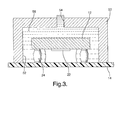
- a microelectronic assembly 10 comprises an integrated circuit die 12 mounted onto a substrate 14 in a flip chip arrangement.
- Substrate 14 is formed of a transparent material.
- a preferred material is glass.
- the substrate may be formed of a polymeric thin film or a polymer glass laminate, such as an FR4 board.
- Die 12 is formed of a semiconductor material, preferably silicon, and comprises an active face 16 that includes a central region 18 surrounded by a perimeter region 20.
- An optical feature 22 is formed on the active face at the central region.
- die 12 may be an digital imaging device that includes, as feature 22, an array of optical sensors and related circuitry for sensing and processing light to produce an image, such as a digital picture.
- feature 22 may be detector for receiving an optical signal, or an element for emitting an optical signal.
- die 12 is attached to substrate 14 by a plurality of solder bump interconnections 24.
- die 12 comprises bond pads 26 distributed about the perimeter region in a perimeter array.
- Substrate 14 includes bond pads 28 in a corresponding arrangement to register with bond pads 26.
- Connections 24 are formed of near-eutectic tin-lead solder alloy or other suitable solder alloy and bond to pads 26 and 28 to attach die 12 to substrate 14.
- Connections 24 are also adapted for transmitting electrical signals to and from die 12 for processing.
- solder bump interconnections are used in the preferred embodiment, the assembly may suitably comprise stud bump connections wherein a bump, typically formed of gold, is affixed to the bond pad on the die and attached to the substrate pad by solder or conductive adhesive.
- bump interconnections refers to solder bump interconnections, stud bump interconnections or other suitable interconnections formed within the gap to mechanically and electrically attach the die to the substrate.
- die 12 is attached such that optical feature 22 faces substrate 14 and is spaced apart by a gap 30.
- assembly 10 further comprises an overmolded polymeric encapsulant 32 to protect die 12 on substrate 14.
- encapsulant 32 forms a continuous body that overlies rear face 34 of die 12 opposite active face 16 and bonds to the surface of substrate 14 about the die.
- the encapsulant 32 may be disposed about the die without covering the rear face.
- encapsulant 32 extends within gap 30 to encapsulate interconnections 24.
- the encapsulant composition suitably comprises particulate inorganic filler, such as silica particles, dispersed in a thermoset polymeric matrix, which is preferably an epoxy polymer.
- the encapsulant in general, it is desired to formulate the encapsulant to contain particulate silica or other filler in an amount, typically between about 75% and 90%, to adjust the CTE to within a desired range.
- the desired CTE is dependent upon the nature of the substrate, and is between about 6 and 10 ppm per C for a preferred glass substrate.
- the high filler content renders the encapsulant opaque.
- the encapsulant commonly includes a carbon powder addition, typically less than 1%, that imparts a black color.
- a suitable encapsulant material is commercially available from Cookson Semiconductor Inc. under the trade designation 200.302B.
- the encapsulant encloses the interconnections 24 within gap 30 and preferably exhibits a CTE comparable to the substrate material.
- die 12 and substrate 14 are subjected to cyclic heating and cooling caused by ambient temperature fluctuations, or as the result of heat generated by the die during operation.
- Encapsulant 32 surrounds the interconnections to reduce stress that would otherwise result from differences in the expansion or contraction of the die and substrate.
- encapsulant 32 also forms a barrier to protect the interconnections from the atmosphere that would otherwise tend to cause corrosion of the solder alloy, and reinforces the interconnections against damage due to vibration or other mechanical forces.
- encapsulant 32 within gap 30 is limited to the perimeter region 18 and does not extend within the central region 18. In this manner, encapsulant 32 defines an optical window 36 adjacent optical feature 22 on die 12. During use, light, indicated by arrow 38, propagates through substrate 14 and through optical window 36 and is received by optical feature 22 for detection and processing. In an alternate embodiment wherein feature 22 emits light, the emitted light is transmitted through window 36 and substrate 14. In any event, the absence of encapsulant material allows the light to be transmitted through the optical window without interference.
- microelectronic assembly 10 is manufactured by initially attaching die 12 to substrate 14 by a flip chip process.
- Suitable flip chip processes are well known.
- a preferred process comprises distributing a microsphere of a suitable solder alloy onto each bond pad 26 on die 12, and heating and cooling the die to reflow the solder and form a solder bump bonded to the die bond pad.
- the die with the solder bumps is then arranged on the substrate such that each bump rests in contact with a corresponding bond pad on the substrate.
- the arrangement is then heated and cooled to bond the solder bump to the bond pad on the substrate, as well as the die, to thereby physically attach the die to the substrate and to concurrently electrically connect the bond pad on the die to the corresponding bond pad on the substrate.
- a mold 50 is positioned about the die on the substrate. Mold 50 engages the substrate about the die attach region, so that the mold and substrate cooperate to form a molding cavity 52.
- a charge of an encapsulant precursor material 56 is injected into cavity 52 through an opening 54 in mold 50.
- the material comprises particulate silica filler dispersed in a liquid phase that contains curable epoxy polymer compound.
- cavity 52 is evacuated prior to injecting the polymeric material to facilitate charging and minimize gas bubbles in the product encapsulant.
- pressure is applied to the material to increase flow into the cavity. The applied pressure initiates flow of the material into the gap about the interconnections.
- the applied pressure is reduced to a second value that limits flow of the material into the gap.
- flow of the material is confined to the perimeter region, and the window is formed adjacent the central region.
- the material is cured within the mold at about 165 °C, thereby forming the encapsulant, whereafter the mold is removed.
- the encapsulant is formed of an epoxy material containing particulate silica filler.
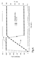
- the charge of precursor material is preheated to 85 °C and 125 °C.
- a pressure of about 600 psi is applied to inject the charge into the cavity.
- the fill rate of the cavity is shown by line 62.
- the applied pressure is rapidly reduced to about 100 psi to complete filling of the cavity.
- the material is heated to about 165 °C to cure the epoxy material and form the product encapsulant.
- a high injection molding pressure to minimize processing time and avoid settling of the particulate filler, thereby producing a uniform encapsulant composition.
- the high applied pressure also produces flow into the underchip gap.
- a pressure of at least about 350 psi to 750 psi is sufficient to inject the material and initiate underchip flow.
- the pressure is reduced to a level that restrict further flow into the gap.
- a pressure less than about 150 psi is suitable to prevent gap fill.
- this invention provides a flip chip microelectronic assembly having an overmolded encapsulant that defines an optical window for transmitting light to and from the active face of the die. Despite the window, the encapsulant extends within the gap sufficient to protect the solder bump interconnections. It is a particular advantage of this invention that the encapsulant material may be formulated to exhibit a coefficient of thermal expansion comparable to the die and substrate. As a result, the encapsulant is effective to reinforce the interconnections to withstand thermally induced stresses due to cyclic heating during use. In commercial materials, adjustment of the coefficient of thermal expansion is accomplished by addition of a filler that renders the encapsulant opaque. Nevertheless, this invention permits use of conventional materials assuring sufficient flow of the encapsulant about the interconnection to provide adequate protection, while forming a widow to assure optical access to the die active face.
Landscapes
- Solid State Image Pick-Up Elements (AREA)
- Structures Or Materials For Encapsulating Or Coating Semiconductor Devices Or Solid State Devices (AREA)
- Encapsulation Of And Coatings For Semiconductor Or Solid State Devices (AREA)
Applications Claiming Priority (2)
| Application Number | Priority Date | Filing Date | Title |
|---|---|---|---|
| US815529 | 2001-03-23 | ||
| US10/815,529 US20050224967A1 (en) | 2004-04-01 | 2004-04-01 | Microelectronic assembly with underchip optical window, and method for forming same |
Publications (2)
| Publication Number | Publication Date |
|---|---|
| EP1583160A2 true EP1583160A2 (de) | 2005-10-05 |
| EP1583160A3 EP1583160A3 (de) | 2008-07-02 |
Family
ID=34887746
Family Applications (1)
| Application Number | Title | Priority Date | Filing Date |
|---|---|---|---|
| EP05075731A Withdrawn EP1583160A3 (de) | 2004-04-01 | 2005-03-29 | Microelektronischer Aufbau mit optischem Fenster auf der Chip-Unterseite und dessen Herstellung |
Country Status (2)
| Country | Link |
|---|---|
| US (2) | US20050224967A1 (de) |
| EP (1) | EP1583160A3 (de) |
Cited By (1)
| Publication number | Priority date | Publication date | Assignee | Title |
|---|---|---|---|---|
| CN110676326A (zh) * | 2018-06-18 | 2020-01-10 | 日月光半导体制造股份有限公司 | 光学封装装置 |
Families Citing this family (11)
| Publication number | Priority date | Publication date | Assignee | Title |
|---|---|---|---|---|
| US20060055032A1 (en) * | 2004-09-14 | 2006-03-16 | Kuo-Chin Chang | Packaging with metal studs formed on solder pads |
| DE102006032073B4 (de) * | 2006-07-11 | 2016-07-07 | Intel Deutschland Gmbh | Elektrisch leitfähiger Verbund aus einem Bauelement und einer Trägerplatte |
| US8519324B2 (en) * | 2006-09-15 | 2013-08-27 | Nec Corporation | Laser projector for projecting and displaying an image based on the raster scanning of a laser beam |
| CN101393922B (zh) * | 2008-10-30 | 2011-06-15 | 旭丽电子(广州)有限公司 | 镜头模组及其制作方法 |
| KR101362398B1 (ko) | 2012-07-10 | 2014-02-13 | 앰코 테크놀로지 코리아 주식회사 | 반도체 패키지 및 그 제조 방법 |
| US20130075894A1 (en) * | 2011-09-23 | 2013-03-28 | Texas Instruments Incorporated | Integrated circuit and method of making |
| CN104040397B (zh) * | 2012-01-31 | 2016-01-27 | 惠普发展公司,有限责任合伙企业 | 用于光电引擎的组合底部填充挡墙和电互连结构 |
| KR102005771B1 (ko) | 2012-02-24 | 2019-10-01 | 삼성전자주식회사 | 무선 통신 네트워크에서 ip 주소 할당 방법 및 장치 |
| US8890274B2 (en) * | 2012-07-11 | 2014-11-18 | Taiwan Semiconductor Manufacturing Company, Ltd. | Interconnect structure for CIS flip-chip bonding and methods for forming the same |
| US11502029B2 (en) * | 2019-07-19 | 2022-11-15 | Stmicroelectronics Pte Ltd | Thin semiconductor chip using a dummy sidewall layer |
| CN116682791A (zh) * | 2022-05-10 | 2023-09-01 | 台湾积体电路制造股份有限公司 | 封装件及其形成方法 |
Family Cites Families (10)
| Publication number | Priority date | Publication date | Assignee | Title |
|---|---|---|---|---|
| EP0840369A4 (de) * | 1995-06-30 | 2001-12-19 | Toshiba Kk | Elektronisches bauteil und herstellungsverfahren dafür |
| US5682066A (en) * | 1996-08-12 | 1997-10-28 | Motorola, Inc. | Microelectronic assembly including a transparent encapsulant |
| JPH1064956A (ja) * | 1996-08-20 | 1998-03-06 | Fujitsu Ltd | フェースダウンボンディング半導体装置 |
| US5895229A (en) * | 1997-05-19 | 1999-04-20 | Motorola, Inc. | Microelectronic package including a polymer encapsulated die, and method for forming same |
| TW460927B (en) * | 1999-01-18 | 2001-10-21 | Toshiba Corp | Semiconductor device, mounting method for semiconductor device and manufacturing method for semiconductor device |
| US6571466B1 (en) * | 2000-03-27 | 2003-06-03 | Amkor Technology, Inc. | Flip chip image sensor package fabrication method |
| US6661084B1 (en) * | 2000-05-16 | 2003-12-09 | Sandia Corporation | Single level microelectronic device package with an integral window |
| US7323360B2 (en) * | 2001-10-26 | 2008-01-29 | Intel Corporation | Electronic assemblies with filled no-flow underfill |
| US6800946B2 (en) * | 2002-12-23 | 2004-10-05 | Motorola, Inc | Selective underfill for flip chips and flip-chip assemblies |
| US7141884B2 (en) * | 2003-07-03 | 2006-11-28 | Matsushita Electric Industrial Co., Ltd. | Module with a built-in semiconductor and method for producing the same |
-
2004
- 2004-04-01 US US10/815,529 patent/US20050224967A1/en not_active Abandoned
-
2005
- 2005-03-29 EP EP05075731A patent/EP1583160A3/de not_active Withdrawn
-
2006
- 2006-09-15 US US11/521,741 patent/US20070007668A1/en not_active Abandoned
Cited By (2)
| Publication number | Priority date | Publication date | Assignee | Title |
|---|---|---|---|---|
| CN110676326A (zh) * | 2018-06-18 | 2020-01-10 | 日月光半导体制造股份有限公司 | 光学封装装置 |
| CN110676326B (zh) * | 2018-06-18 | 2023-07-18 | 日月光半导体制造股份有限公司 | 光学封装装置 |
Also Published As
| Publication number | Publication date |
|---|---|
| EP1583160A3 (de) | 2008-07-02 |
| US20050224967A1 (en) | 2005-10-13 |
| US20070007668A1 (en) | 2007-01-11 |
Similar Documents
| Publication | Publication Date | Title |
|---|---|---|
| US8034652B2 (en) | Solid state imaging device and manufacturing method thereof | |
| US6774481B2 (en) | Solid-state image pickup device | |
| US6191360B1 (en) | Thermally enhanced BGA package | |
| US7135769B2 (en) | Semiconductor packages and methods of manufacturing thereof | |
| US20050224967A1 (en) | Microelectronic assembly with underchip optical window, and method for forming same | |
| US7321455B2 (en) | Microelectronic devices and methods for packaging microelectronic devices | |
| EP1861880B1 (de) | Verfahren zur herstellung eines halbleiter-bildgebungsbauelements | |
| CN103915393B (zh) | 光电封装体及其制造方法 | |
| US6034333A (en) | Frame embedded in a polymeric encapsulant | |
| US8680669B2 (en) | Electronic component, electronic module, and method for manufacturing the same | |
| US20080061447A1 (en) | Wire-bonded package with electrically insulating wire encapsulant and thermally conductive overmold | |
| CN1192041A (zh) | 半导体器件的制造方法 | |
| US20030234452A1 (en) | Optical integrated circuit element package and process for making the same | |
| US6972497B2 (en) | Optical semiconductor device and method of manufacture | |
| US20060256222A1 (en) | CIS Package and Method Thereof | |
| KR20080023996A (ko) | 반도체 패키지 | |
| US7776648B2 (en) | High thermal performance packaging for circuit dies | |
| US20070178627A1 (en) | Flip-chip semiconductor device and method for fabricating the same | |
| KR102081612B1 (ko) | 반도체 패키지 및 이것의 제조 방법 | |
| US20080315405A1 (en) | Heat spreader in a flip chip package | |
| KR100674501B1 (ko) | 플립 칩 본딩 기술을 이용한 반도체 칩 실장 방법 | |
| CN111370337A (zh) | 降低封装翘曲方法 | |
| CN107637186A (zh) | 具有用于传动装置控制单元的阿尔法射线保护的电子装置模块以及传动装置控制单元 | |
| US6629633B1 (en) | Chip size image sensor bumped package fabrication method | |
| US20090179290A1 (en) | Encapsulated imager packaging |
Legal Events
| Date | Code | Title | Description |
|---|---|---|---|
| PUAI | Public reference made under article 153(3) epc to a published international application that has entered the european phase |
Free format text: ORIGINAL CODE: 0009012 |
|
| AK | Designated contracting states |
Kind code of ref document: A2 Designated state(s): AT BE BG CH CY CZ DE DK EE ES FI FR GB GR HU IE IS IT LI LT LU MC NL PL PT RO SE SI SK TR |
|
| AX | Request for extension of the european patent |
Extension state: AL BA HR LV MK YU |
|
| PUAL | Search report despatched |
Free format text: ORIGINAL CODE: 0009013 |
|
| AK | Designated contracting states |
Kind code of ref document: A3 Designated state(s): AT BE BG CH CY CZ DE DK EE ES FI FR GB GR HU IE IS IT LI LT LU MC NL PL PT RO SE SI SK TR |
|
| AX | Request for extension of the european patent |
Extension state: AL BA HR LV MK YU |
|
| 17P | Request for examination filed |
Effective date: 20090105 |
|
| AKX | Designation fees paid |
Designated state(s): AT BE BG CH CY CZ DE DK EE ES FI FR GB GR HU IE IS IT LI LT LU MC NL PL PT RO SE SI SK TR |
|
| 17Q | First examination report despatched |
Effective date: 20090423 |
|
| STAA | Information on the status of an ep patent application or granted ep patent |
Free format text: STATUS: THE APPLICATION IS DEEMED TO BE WITHDRAWN |
|
| 18D | Application deemed to be withdrawn |
Effective date: 20090904 |