EP1580871A1 - Quasi-aktive leistungsfaktorkorrekturschaltung f r ein schaltnetzteil - Google Patents
Quasi-aktive leistungsfaktorkorrekturschaltung f r ein schaltnetzteil Download PDFInfo
- Publication number
- EP1580871A1 EP1580871A1 EP03769171A EP03769171A EP1580871A1 EP 1580871 A1 EP1580871 A1 EP 1580871A1 EP 03769171 A EP03769171 A EP 03769171A EP 03769171 A EP03769171 A EP 03769171A EP 1580871 A1 EP1580871 A1 EP 1580871A1
- Authority
- EP
- European Patent Office
- Prior art keywords
- converter
- current
- input
- voltage
- power factor
- Prior art date
- Legal status (The legal status is an assumption and is not a legal conclusion. Google has not performed a legal analysis and makes no representation as to the accuracy of the status listed.)
- Withdrawn
Links
Images






Classifications
-
- H—ELECTRICITY
- H02—GENERATION; CONVERSION OR DISTRIBUTION OF ELECTRIC POWER
- H02M—APPARATUS FOR CONVERSION BETWEEN AC AND AC, BETWEEN AC AND DC, OR BETWEEN DC AND DC, AND FOR USE WITH MAINS OR SIMILAR POWER SUPPLY SYSTEMS; CONVERSION OF DC OR AC INPUT POWER INTO SURGE OUTPUT POWER; CONTROL OR REGULATION THEREOF
- H02M1/00—Details of apparatus for conversion
- H02M1/42—Circuits or arrangements for compensating for or adjusting power factor in converters or inverters
- H02M1/4208—Arrangements for improving power factor of AC input
- H02M1/425—Arrangements for improving power factor of AC input using a single converter stage both for correction of AC input power factor and generation of a high frequency AC output voltage
-
- H—ELECTRICITY
- H02—GENERATION; CONVERSION OR DISTRIBUTION OF ELECTRIC POWER
- H02M—APPARATUS FOR CONVERSION BETWEEN AC AND AC, BETWEEN AC AND DC, OR BETWEEN DC AND DC, AND FOR USE WITH MAINS OR SIMILAR POWER SUPPLY SYSTEMS; CONVERSION OF DC OR AC INPUT POWER INTO SURGE OUTPUT POWER; CONTROL OR REGULATION THEREOF
- H02M3/00—Conversion of DC power input into DC power output
- H02M3/22—Conversion of DC power input into DC power output with intermediate conversion into AC
- H02M3/24—Conversion of DC power input into DC power output with intermediate conversion into AC by static converters
- H02M3/28—Conversion of DC power input into DC power output with intermediate conversion into AC by static converters using discharge tubes with control electrode or semiconductor devices with control electrode to produce the intermediate AC
- H02M3/325—Conversion of DC power input into DC power output with intermediate conversion into AC by static converters using discharge tubes with control electrode or semiconductor devices with control electrode to produce the intermediate AC using devices of a triode or a transistor type requiring continuous application of a control signal
- H02M3/335—Conversion of DC power input into DC power output with intermediate conversion into AC by static converters using discharge tubes with control electrode or semiconductor devices with control electrode to produce the intermediate AC using devices of a triode or a transistor type requiring continuous application of a control signal using semiconductor devices only
-
- Y—GENERAL TAGGING OF NEW TECHNOLOGICAL DEVELOPMENTS; GENERAL TAGGING OF CROSS-SECTIONAL TECHNOLOGIES SPANNING OVER SEVERAL SECTIONS OF THE IPC; TECHNICAL SUBJECTS COVERED BY FORMER USPC CROSS-REFERENCE ART COLLECTIONS [XRACs] AND DIGESTS
- Y02—TECHNOLOGIES OR APPLICATIONS FOR MITIGATION OR ADAPTATION AGAINST CLIMATE CHANGE
- Y02B—CLIMATE CHANGE MITIGATION TECHNOLOGIES RELATED TO BUILDINGS, e.g. HOUSING, HOUSE APPLIANCES OR RELATED END-USER APPLICATIONS
- Y02B70/00—Technologies for an efficient end-user side electric power management and consumption
- Y02B70/10—Technologies improving the efficiency by using switched-mode power supplies [SMPS], i.e. efficient power electronics conversion e.g. power factor correction or reduction of losses in power supplies or efficient standby modes
Definitions
- the present invention is relative to single phase AC to DC converter with power factor correction function (so that the power factor of the input current is at a power factor in excess of that of an otherwise comparable low-power-factor converter design). It can be used on in switching mode power supply and electronics ballast.
- PFC power factor correction
- PFC circuits are classified into two groups. First group is defined as active PFC circuits, and second group is defined as passive PFC circuits.
- the very popular Boost-type PFC circuit is an active PFC circuit. It can shape the input current and make the total harmonic distortion (THD) very low.
- THD total harmonic distortion
- the efficiency of the active PFC circuit is lower than one of passive PFC circuit, due to extra switching circuit.
- the control of the active PFC is complicated, resulting in increased manufacturing cost and reduced reliability of the circuit.
- the passive PFC due to no active control switch in the circuit, the passive PFC can work in higher efficiency, but THD of the passive PFC is higher and size of the passive components is big.
- the concept of single power stage converter with PFC was presented for several years.
- some extra passive components are added to a regular converter.
- the extra components are working in the converter's switching frequency.
- the size of the extra component is small due to higher operating switching frequency.
- the main task of the active switch of the converter is to regulate the output power.
- the active switch involves a part of task to shape the input current. Due to both input and output current controlled by the active switch, the loss on the active switch is higher and the efficiency of the whole system is lower.
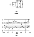
- valley-fill circuit Based on the existed PFC circuits, there are a lot of papers and patents about valley-fill circuit. The basic valley-fill circuit is shown in Fig.1. Valley-fill circuit can provide better performance than other passive types of PFC circuits.
- the power line directly feeds energy (e.g. electrical energy) to the load through the rectifier diodes for approximately 120 degrees around the peek voltage.
- energy e.g. electrical energy
- Two storage capacitors C1 and C2 feed energy to the load through diodes D1 and D2 for approximately 60 degrees near the zero line crossing points.
- Most of the input energy being first fed to the load, with a small portion of the input energy being first fed to the two storage capacitors C1 and C2, and then fed to the load through capacitors C1 and C2.
- energy e.g. electrical energy
- valley-fill circuit Problems with the valley-fill circuit are a pulsating line current charges the capacitors near the peak power line voltage, resulting in a deteriorated PF (of about 0.95) and a high THD (e.g. about 40%).
- the output of the valley-fill circuit exhibits a large ripple from the half of the power line peak voltage to the power line peak voltage, with the ripple frequency being equal to twice the line frequency.
- Japanese Pat. No. HEI 8-205520 illustrated in Fig.5 describes the load current of a PFC converter as being discontinuous, and discloses that the insertion of a suitable inductor L1 in the input power line avoids pulsating of the power line current. Because an instantaneous line voltage is higher than the voltage of each DC bulk capacitor C1 and C2, while being less than the sum of the voltages of the two capacitors, the inserted inductor provides a boost function to boost the sum of the voltage of the two capacitors.
- this disclosure fails to solve the above-described problem that exists at the input current during the approximate 60 degree dead time near the zero line crossing points.
- U.S. Pat. No. 5,986,901 illustrated in Fig.6 discloses the use of the high frequency discontinuous input current of the converter to drive a charge pump circuit Z and the inserted input inductor.
- the charge pump circuit shapes the input current during the approximate 60 degree dead time, and the input inductor provides a boost function to boost the sum of the voltage of the two capacitors. Because the charge pump circuit and the inserted input inductor are driven with the discontinuous input current automatically, the active switch or switches in the converter would not be exposed to extra current or voltage stresses.
- the disclosure needs several passive components to implement the charge pump circuit. The cost of the disclosure is still high.
- the present invention is based on a valley-fill circuit, but the 60 degree dead time and the pulsating current of the valley-fill PFC circuit are eliminated, while maintaining a high operating efficiency.
- an energy storage device such as, for example, a coupled inductor circuit
- the coupled inductor circuit is employed to reduce (or eliminate) the power line's pulsating line current and to help boost performance of the auxiliary PFC circuit.
- the present invention enables one to avoid the use of active switch and control circuit for a PFC while keeping the advantages of a passive PFC circuit; namely, high efficiency, resulting in a lowered manufacturing cost.
- the PFC function automatically acts when the line voltage is less than the voltage on a pair of the storage capacitors.
- a power factor correction circuit includes a system that shapes an input current of a power line during predetermined period proximate a zero line crossing point of the input voltage, and a system that minimizes a pulsating of the input current.
- an output of the power factor correction circuit is provided to a discontinuous power source, such as, for example, a discontinuous current load that is suitable for most power converter circuits as a following power stage, a discontinuous current input buck converter, a discontinuous current input full bridge converter, a discontinuous current input full bridge inverter, a discontinuous current input half bridge converter, a discontinuous current input half bridge inverter, or a discontinuous current input buck-boost converter, a discontinuous current input flyback converter.
- a discontinuous current load such as, for example, a discontinuous current load that is suitable for most power converter circuits as a following power stage, a discontinuous current input buck converter, a discontinuous current input full bridge converter, a discontinuous current input full bridge inverter, a discontinuous current input half bridge converter, a discontinuous current input half bridge inverter, or a discontinuous current input buck-boost converter, a discontinuous current input flyback converter.
- the coupled inductor circuit comprises a multi-winding coupled inductor on one magnetic core.
- One winding of the coupled inductor is connected between the output of the rectifier and the valley-fill PFC converter as well as the output load of the valley-fill PFC converter.
- At least a second winding of the coupled inductor is connected to at least one DC bulk storage capacitance device of the valley-fill PFC converter.
- the current released from the DC bulk storage capacitance device of the valley-fill PFC converter can be stored in magnetic energy in the coupled inductor and as the output load current of the valley-fill PFC converter is zero, that is, discontinuous, the energy stored in the coupled inductor will release to the two DC bulk storage capacitance devices of the valley-fill PFC converter and other energy storage device through the rectifier and input AC line of the valley-fill PFC converter during the approximate 60 degree dead time.
- a switching power supply having an AC-to-DC converting device that converts an AC input line voltage to a DC voltage, an energy storage device (such as, for example, a valley-fill circuit and other energy storage device) that stores electrical energy in which the stored energy is released to a load during a predetermined period of the AC input line voltage, and an auxiliary power factor corrector that operates, after a release of the electrical energy (such as, for example, a high frequency discontinuous current), stored in the energy storage device, to shape the AC input line current during the predetermined period.
- the predetermined period comprises a period proximate a zero voltage crossing of the AC input voltage.
- a device which limits the current slew rate that limits a current input slew rate of the AC-DC converter device.
- the current slew rate limiting device comprises an electromotive force generator, such as, for example, the couple inductors.
- the present invention discloses a passive PFC circuit that exhibits a high operating efficiency.
- a block diagram of a preferred embodiment is shown in Fig. 7.
- a driving source of an auxiliary PFC circuit Z such as, for example, a coupled inductor is coupled to at least one leg of the valley-fill circuit to shape the input current during the 60 degree dead time near the zero line crossing points.
- the load of PFC converter comprises a discontinuous current source that exhibits a minimum dead time. During the dead time, the load current is zero or negative.
- the auxiliary PFC's driving source is coupled from at least one leg of the valley-fill circuit.
- the leg (or legs) is (are) composed of a pair of diodes and a pair of DC bulk capacitors.
- the driving source couple from the legs is a high frequency unipolar current source due to the series diodes.
- Fig. 8 illustrates a circuit of the preferred embodiment of the present invention.
- the preferred embodiment of the present invention comprises a differential filter made up of inductor Lf and capacitor Cf, a bridge rectifier BR, an inserted electromotive force generating device (such as, for example, a coupled inductor C_Inductor with three windings L1, L2 and L3), three valley-fill diodes D1, D2 and D3, two DC bulk capacitors C1 and C2, a resonant capacitor Cr and a discontinuous power source, such as, for example, a buck, a buck-boost, a forward, a flyback, a resonant inverter circuit, or any other equivalent discontinuous power load.
- a discontinuous power source such as, for example, a buck, a buck-boost, a forward, a flyback, a resonant inverter circuit, or any other equivalent discontinuous power load.
- the auxiliary PFC circuit comprises the coupled inductor with three windings.
- the coupled inductor's windings couple the driving source from the legs of the valley-fill circuit to shape the input current through the coupled inductor's magnetic field.
- the coupled inductor is also used to limit (minimize) the slew rate of the pulsating current and to serve as a boost function to help PFC performance.
- the discontinuous power (current) load is generated by the switching converter, such as, for example, a buck converter, a buck-boost converter, a flyback converter, a forward converter, a resonant converter, or any other type of switching converter.
- the switching converter such as, for example, a buck converter, a buck-boost converter, a flyback converter, a forward converter, a resonant converter, or any other type of switching converter.
- a direct feed mode (corresponding to a situation in which an instantaneous input line voltage is higher than the voltage of each DC bulk capacitor C1 and C2)
- a couple boost mode (corresponding to a situation in which an instantaneous input line voltage is lower than the voltage of each DC bulk capacitor C1 and C2).
- the output voltage of the rectifier bridge is higher than the voltage on each DC bulk capacitors C1 and C2, but less than the sum of voltage on each DC bulk capacitors C1 and C2.
- the input line will directly feed the energy to the load and the resonant capacitor Cr through C_inductor's winding L1 and the rectifier. Because the load current passes through L1 and the bridge rectifier BR, there is energy stored in L1. As the load current is changed from the fixed value down to zero, the energy stored in L 1 will release to the resonant capacitor Cr and two DC bulk capacitors C1 and C2 in series through D3.
- each switching period can be divided as two intervals. During the first interval, the input power line will directly feed the energy to the load and store the energy in L1. During the second interval, the input power line will charge the resonant capacitor Cr and two DC bulk capacitors through C_Inductor's winding L1 and D3.
- Couple Boost mode
- the input AC voltage is lower than the voltage on each DC bulk capacitor. Because the input AC voltage is lower than the voltage on each DC bulk capacitor, as the load current is changed from zero to a fixed value, the resonant capacitor Cr releases the stored energy and the voltage on Cr decreases. As the voltage on Cr is less than the voltage of the two DC bulk capacitors, the two DC bulk capacitors C1 and C2 will release the stored energy to the load and the resonant capacitor Cr in parallel.
- the current passes through windings L2 and L3 of the coupled inductor C_Inductor. Energy is stored in the coupled inductor C_Inductor windings. It is coupled inductor C _Inductor that resonates with the resonant capacitor Cr.
- the coupled inductor windings L2 and L3 continue to resonate with Cr.
- the voltage on Cr increases.
- diodes D1 and D2 turn off and the stored magnetic energy in the coupled inductor is transferred from the windings L2 and L3 to the winding L1.
- the coupled inductor C_Inductor will release the stored magnetic energy to the resonant capacitor Cr and bulk DC capacitors C1, C2 through C_Inductor's winding L1.
- the input power line will also release or feed energy to the resonant capacitor Cr and bulk DC capacitors C1, C2.
- each switching period can also be divided as three intervals.
- two DC bulk capacitors C1 and C2 release the stored energy to the load and store the energy in C_Inductor windings L2 and L3.
- the windings L2 and L3 resonate with the resonant capacitor Cr to transfer the stored magnetic energy from the windings L2 and L3 to the winding L1.
- the coupled inductor's stored energy and the input power line will charge the resonant capacitor Cr and bulk DC capacitors C1 and C2 through the coupled inductor C_Inductor's winding L1.
- the problem of the input current during the 60 degree dead-time near the zero line crossings can be solved. Because the currents in the branches of D1 and D2 are discontinuous, it is possible to use a high frequency coupled inductor coupled to a unipolar high frequency current source, having an instant current that varies from a fixed value to zero. There is current through D1 and D2 only during the 60 degree dead time, and the couple boost mode automatically works during that period to shape the input current. The circuit's circulating current is low. It is the L1's winding current that can be used to absorb the input energy from the power line as the instantaneous output voltage of the rectifier is lower than that of C1 or C2.
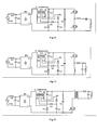
- a buck circuit 100 is provided as a following power stage, in which the buck circuit works in a continuous or discontinuous current mode.
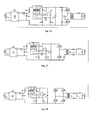
- Fig.10 illustrates a third embodiment of the present invention.
- a discharge lamp such as, for example, a high intensity discharge (HID) lamp is driven by the PFC converter.
- a full bridge inverter 200 outputs a low frequency square AC current source.
- Fig. 11 illustrates a fourth embodiment of the present invention.
- a half bridge 300 is employed (used) to drive the discharge lamp, such as, for example, a fluorescent lamp, with a high frequency sinusoidal AC current.
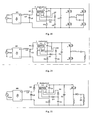
- Fig. 12 to 18 illustrate the fifth, sixth, seventh, eighth, ninth, tenth and eleventh embodiments of the present invention.
- the PFC converter is interfaced to a discontinuous current input buck-boost converter 400.
- the sixth embodiment illustrates the PFC converter of the present invention being interfaced to a discontinuous current input flyback converter 500.
- the seventh embodiment illustrates the PFC converter of the present invention being interfaced to a discontinuous current input forward converter 600.
- the eighth embodiment (Fig.15) illustrates the PFC converter of the present invention being interfaced to a two-switch forward converter 700.
- the ninth embodiment illustrates the PFC converter of the present invention being interfaced to a two-switch flyback converter 800.
- the tenth embodiment illustrates the PFC converter of the present invention being interfaced to a half-bridge DC-DC converter 900.
- the eleventh embodiment illustrates the PFC converter of the present invention being interfaced to a full-bridge DC-DC converter 1000.
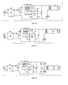
- Fig. 19 to 28 illustrate the modified topologies shown in Fig.9 to Fig.18, that is, the low pass filters are shifted from AC side to DC side.
- the diode Df is inserted to make the current in L1 unipolar.
- the benefit of low pass filter in DC side is that the rectifier can be low speed.
- Fig. 31 illustrates the modified topology for the topology shown in Fig.8.
- the operation concept is the same.
- the difference of two topologies is the multi-winding couple inductor C_Inductor.
- the couple inductor has three separated windings.
- the couple inductor has two separated windings but one winding has a tapping.
- the couple coefficiency can be higher and the manufacture cost can be lower. All circuits shown in Fig. 9 to Fig. 18 can use the circuit shown in Fig. 31 for power factor correction function.
- Fig. 32 illustrates the modified topologies shown in Fig.8, that is, the low pass filters are shifted from AC side to DC side. As the low pass filter is shifted from AC side to DC side, the diode Df is inserted to make the current in L1 unipolar. All circuits shown in Fig.19 to Fig. 28 can use the circuit shown in Fig.32 for power factor correction function.
- the present invention provides several significant improvements over prior art devices.
- the PFC converter of the present invention provides an improved PFC function, as compared to prior art.
- the present invention does not impose any additional current or voltage stresses on the switches.
- the improved valley-fill power stage of the instant invention is passive and fewer additional components. As a result, the efficiency and reliability of the PFC stage of the present invention is very high and the manufacture cost is low.
Landscapes
- Engineering & Computer Science (AREA)
- Power Engineering (AREA)
- Dc-Dc Converters (AREA)
- Rectifiers (AREA)
Applications Claiming Priority (3)
| Application Number | Priority Date | Filing Date | Title |
|---|---|---|---|
| US287828 | 2002-11-05 | ||
| US10/287,828 US6909622B2 (en) | 2002-11-05 | 2002-11-05 | Quasi active power factor correction circuit for switching power supply |
| PCT/CN2003/000930 WO2004042903A1 (en) | 2002-11-05 | 2003-11-03 | A quasi-active power factor correction circuit for switching power supply |
Publications (2)
| Publication Number | Publication Date |
|---|---|
| EP1580871A1 true EP1580871A1 (de) | 2005-09-28 |
| EP1580871A4 EP1580871A4 (de) | 2006-03-01 |
Family
ID=32175765
Family Applications (1)
| Application Number | Title | Priority Date | Filing Date |
|---|---|---|---|
| EP03769171A Withdrawn EP1580871A4 (de) | 2002-11-05 | 2003-11-03 | Quasi-aktive leistungsfaktorkorrekturschaltung f r ein schaltnetzteil |
Country Status (5)
| Country | Link |
|---|---|
| US (1) | US6909622B2 (de) |
| EP (1) | EP1580871A4 (de) |
| AU (1) | AU2003280554A1 (de) |
| TW (1) | TW200633356A (de) |
| WO (1) | WO2004042903A1 (de) |
Families Citing this family (35)
| Publication number | Priority date | Publication date | Assignee | Title |
|---|---|---|---|---|
| DE102004001618A1 (de) * | 2004-01-09 | 2005-08-11 | Patent-Treuhand-Gesellschaft für elektrische Glühlampen mbH | Schaltungsanordnung zum Betrieb von Lichtquellen |
| US7541746B2 (en) * | 2005-09-15 | 2009-06-02 | Infocus Corporation | Lamp driver circuit with power factor correction circuit coupled to direct-current to direct-current power converter |
| US7719202B2 (en) * | 2006-10-23 | 2010-05-18 | Zippy Technology Corp. | Light emitting diode driving circuit |
| US7436128B2 (en) * | 2006-10-23 | 2008-10-14 | Zippy Technology Corp. | Driving circuit for hot cathode fluorescent lamps |
| US9108263B2 (en) * | 2007-04-30 | 2015-08-18 | Illinois Tool Works Inc. | Welding power source with automatic variable high frequency |
| WO2009134756A1 (en) * | 2008-04-29 | 2009-11-05 | Cirrus Logic, Inc. | Cascaded switching power converter for coupling a photovoltaic energy source to power mains |
| CN102132628B (zh) * | 2008-08-25 | 2014-03-12 | 马克西姆综合产品公司 | 固态照明装置中的功率因数校正和固态照明装置的调光 |
| TWI381619B (zh) * | 2009-04-01 | 2013-01-01 | Delta Electronics Inc | 單相與三相雙重升降壓功率因數校正電路及其控制方法 |
| US7923862B2 (en) * | 2009-10-06 | 2011-04-12 | General Electric Company | Reactive power regulation and voltage support for renewable energy plants |
| US9466984B2 (en) * | 2009-10-26 | 2016-10-11 | General Electric Company | Power ramp rate control for renewable variable power generation systems |
| US8773085B2 (en) | 2011-03-22 | 2014-07-08 | Ledillion Technologies Inc. | Apparatus and method for efficient DC-to-DC conversion through wide voltage swings |
| TWI437410B (zh) | 2011-09-30 | 2014-05-11 | Ind Tech Res Inst | 降壓式功率因數修正系統 |
| KR20130134786A (ko) * | 2012-05-31 | 2013-12-10 | 주식회사 실리콘웍스 | Led 램프 구동을 위한 전원 회로 및 전원 공급 방법 그리고 플라이백 트랜스포머의 일차측 제어 회로 |
| TWI477044B (zh) * | 2012-08-10 | 2015-03-11 | Univ Nat Kaohsiung Marine | Step-down rectifier |
| TWI469479B (zh) * | 2012-08-27 | 2015-01-11 | Ind Tech Res Inst | 被動式功率因數校正電路、應用其之電子裝置與其操作方法 |
| PT2923531T (pt) * | 2012-11-21 | 2023-08-17 | Versitech Ltd | Controlador para iluminação led e método de controlo de iluminação led |
| TWI466421B (zh) * | 2012-12-05 | 2014-12-21 | Hep Tech Co Ltd | Method of Activation Method of Passive AC and DC Converter and Its Function Correction Circuit |
| CN103856077B (zh) * | 2012-12-06 | 2016-12-21 | 东林科技股份有限公司 | 被动式功因校正交直流转换装置的功因校正电路的动作方法 |
| US9214855B2 (en) | 2013-05-03 | 2015-12-15 | Cooper Technologies Company | Active power factor correction circuit for a constant current power converter |
| US9000736B2 (en) | 2013-05-03 | 2015-04-07 | Cooper Technologies Company | Power factor correction algorithm for arbitrary input waveform |
| US9190901B2 (en) | 2013-05-03 | 2015-11-17 | Cooper Technologies Company | Bridgeless boost power factor correction circuit for constant current input |
| US9548794B2 (en) | 2013-05-03 | 2017-01-17 | Cooper Technologies Company | Power factor correction for constant current input with power line communication |
| WO2015103641A1 (en) * | 2014-01-06 | 2015-07-09 | Maxat Touzelbaev | Valley-fill power factor correction circuit with active conduction angle control |
| CN104113201A (zh) * | 2014-07-07 | 2014-10-22 | 魏其萃 | 高功率因数低总谐波失真准有源功率因数校正电路及方法 |
| US10270253B2 (en) | 2015-05-14 | 2019-04-23 | Varentec, Inc. | System and method for regulating the reactive power flow of one or more inverters coupled to an electrical grid |
| CN104981065A (zh) * | 2015-06-23 | 2015-10-14 | 成都亿信标准认证集团有限公司 | 具有填谷电路的led驱动装置 |
| CN105162315B (zh) * | 2015-08-21 | 2017-09-29 | 魏其萃 | 电荷泵式低总谐波失真高功率因数校正装置及方法 |
| CN108254675A (zh) * | 2018-03-14 | 2018-07-06 | 奥克斯空调股份有限公司 | Pfc电路故障检测装置、方法及变频空调 |
| CN110289755B (zh) * | 2019-06-26 | 2021-04-06 | 南京理工大学 | 高功率因数DCM Buck-Flyback PFC变换器 |
| WO2021263231A1 (en) * | 2020-06-26 | 2021-12-30 | Ohmium International, Inc. | Impedance monitoring of a modular electrolysis system |
| CN112688554B (zh) * | 2021-03-12 | 2021-07-02 | 深圳原能电器有限公司 | 一种单级pfc变换器及控制方法 |
| US12597616B2 (en) | 2022-01-19 | 2026-04-07 | Ohmium International, Inc. | System and method for controlling hydrogen stack current and load |
| US12470062B2 (en) | 2022-04-18 | 2025-11-11 | Ohmium International, Inc. | Frequency droop to coordinate hydrogen production |
| US12394991B2 (en) | 2022-10-14 | 2025-08-19 | Ohmium International, Inc. | Systems and circuits for connecting components of a hydrogen plant to a power source |
| CN118249638B (zh) * | 2024-03-26 | 2024-11-05 | 西南交通大学 | 无输入电流死区的混合模态无桥降压型pfc变换器 |
Family Cites Families (13)
| Publication number | Priority date | Publication date | Assignee | Title |
|---|---|---|---|---|
| US3913002A (en) * | 1974-01-02 | 1975-10-14 | Gen Electric | Power circuits for obtaining a high power factor electronically |
| JPH08196077A (ja) * | 1994-11-18 | 1996-07-30 | Toshiba Corp | 電力変換装置及びこれを利用した空気調和装置 |
| CN1187749A (zh) * | 1996-12-23 | 1998-07-15 | 通用电气公司 | 具有功率因数校正的气体放电灯镇流器 |
| US6038146A (en) * | 1997-06-13 | 2000-03-14 | Computer Products, Incorporated | High power factors, single stage harmonics correction converter |
| US6118673A (en) * | 1998-06-01 | 2000-09-12 | Virginia Power Technologies, Inc. | Single-stage AC/DC converters with saturable conductor PFC |
| US5986901A (en) * | 1998-07-09 | 1999-11-16 | Matsushita Electric Works R&D Laboratory, Inc. | Power factor correction circuit for a power supply |
| US6023037A (en) * | 1998-11-05 | 2000-02-08 | Lincoln Global, Inc. | Electric ARC welder and plasma cutter |
| TW431059B (en) * | 1999-01-04 | 2001-04-21 | Skynet Electronic Co Ltd | Power factor correction circuit |
| DE19946242A1 (de) * | 1999-09-27 | 2001-04-05 | Grundfos As | Frequenzumrichter für einen Elektromotor |
| US6751104B2 (en) * | 2000-02-02 | 2004-06-15 | The Regents Of The University Of California | Single-stage power factor correction method to reduce energy storage capacitor voltage and circuit for same |
| EP1178710B1 (de) * | 2000-02-14 | 2008-09-10 | Mitsubishi Denki Kabushiki Kaisha | Starter fuer entladungslampe und beleuchtungsanlage |
| CN1114987C (zh) * | 2000-10-19 | 2003-07-16 | 南京航空航天大学 | 新型单级功率因数校正交/直变换器 |
| JP3987949B2 (ja) * | 2001-02-26 | 2007-10-10 | サンケン電気株式会社 | 交流直流変換回路 |
-
2002
- 2002-11-05 US US10/287,828 patent/US6909622B2/en not_active Expired - Fee Related
-
2003
- 2003-11-03 EP EP03769171A patent/EP1580871A4/de not_active Withdrawn
- 2003-11-03 AU AU2003280554A patent/AU2003280554A1/en not_active Abandoned
- 2003-11-03 WO PCT/CN2003/000930 patent/WO2004042903A1/zh not_active Ceased
-
2005
- 2005-03-15 TW TW094107760A patent/TW200633356A/zh unknown
Also Published As
| Publication number | Publication date |
|---|---|
| AU2003280554A1 (en) | 2004-06-07 |
| EP1580871A4 (de) | 2006-03-01 |
| US6909622B2 (en) | 2005-06-21 |
| TW200633356A (en) | 2006-09-16 |
| US20040085788A1 (en) | 2004-05-06 |
| WO2004042903A1 (en) | 2004-05-21 |
Similar Documents
| Publication | Publication Date | Title |
|---|---|---|
| US6909622B2 (en) | Quasi active power factor correction circuit for switching power supply | |
| US5986901A (en) | Power factor correction circuit for a power supply | |
| JP3697915B2 (ja) | 電子バラスト回路 | |
| CN108539984B (zh) | 开关电源电路的pfwm控制系统 | |
| CN1156200C (zh) | 镇流系统 | |
| CN108390555B (zh) | 用于Boost与桥式DC-DC转换电路组合的开关电源的PFWM控制方法 | |
| US20020011801A1 (en) | Power feedback power factor correction scheme for multiple lamp operation | |
| CN111478600A (zh) | 一种用于双有源桥式单级ac-dc变换器的控制方法 | |
| CN101136584B (zh) | 一种降低开关损耗的单级功率因数校正电路 | |
| CN1064178A (zh) | 高功率因数电源 | |
| CN109661072B (zh) | Llc谐振变换器、led驱动电路及其控制方法 | |
| CN101588139A (zh) | 高功率因数隔离降压型功率因数校正变换器 | |
| KR102664416B1 (ko) | 브릿지리스 pfc 컨버터와 위상 천이 풀브릿지 dc-dc 컨버터가 통합된 ac-dc 컨버터 | |
| CN100514807C (zh) | 一种降低emi的单级功率因数校正电路 | |
| CN111740622B (zh) | 一种单级pfc的llc电路 | |
| CN105978327A (zh) | 一种升压变换器及其控制方法 | |
| JP2000003798A (ja) | 放電ランプ点灯装置および照明装置 | |
| CN209930559U (zh) | Llc谐振变换器和led驱动电路 | |
| CN109194165A (zh) | 交流-直流功率变换器 | |
| KR20220081108A (ko) | 브릿지리스 pfc 컨버터와 공진형 dc-dc 컨버터가 통합된 ac-dc 컨버터 | |
| CN112689363A (zh) | 电源转换器 | |
| CN100473251C (zh) | 荧光灯的调光控制装置与方法 | |
| JPH02202365A (ja) | 電源装置 | |
| JP4527959B2 (ja) | 高周波インバータ装置 | |
| JPH0678537A (ja) | スイッチング電源装置 |
Legal Events
| Date | Code | Title | Description |
|---|---|---|---|
| PUAI | Public reference made under article 153(3) epc to a published international application that has entered the european phase |
Free format text: ORIGINAL CODE: 0009012 |
|
| 17P | Request for examination filed |
Effective date: 20050523 |
|
| AK | Designated contracting states |
Kind code of ref document: A1 Designated state(s): AT BE BG CH CY CZ DE DK EE ES FI FR GB GR HU IE IT LI LU MC NL PT RO SE SI SK TR |
|
| AX | Request for extension of the european patent |
Extension state: AL LT LV MK |
|
| DAX | Request for extension of the european patent (deleted) | ||
| A4 | Supplementary search report drawn up and despatched |
Effective date: 20060118 |
|
| RIC1 | Information provided on ipc code assigned before grant |
Ipc: H02M 3/335 20060101ALI20060112BHEP Ipc: G05F 1/70 20060101ALI20060112BHEP Ipc: H02M 1/00 20060101AFI20040525BHEP |
|
| 17Q | First examination report despatched |
Effective date: 20100504 |
|
| STAA | Information on the status of an ep patent application or granted ep patent |
Free format text: STATUS: THE APPLICATION IS DEEMED TO BE WITHDRAWN |
|
| 18D | Application deemed to be withdrawn |
Effective date: 20100915 |