EP1580864A1 - Mobiles Gerät mit Bildsensoren zum Laden einer Batterie - Google Patents
Mobiles Gerät mit Bildsensoren zum Laden einer Batterie Download PDFInfo
- Publication number
- EP1580864A1 EP1580864A1 EP05251035A EP05251035A EP1580864A1 EP 1580864 A1 EP1580864 A1 EP 1580864A1 EP 05251035 A EP05251035 A EP 05251035A EP 05251035 A EP05251035 A EP 05251035A EP 1580864 A1 EP1580864 A1 EP 1580864A1
- Authority
- EP
- European Patent Office
- Prior art keywords
- image sensor
- battery
- pixels
- mobile device
- battery charger
- Prior art date
- Legal status (The legal status is an assumption and is not a legal conclusion. Google has not performed a legal analysis and makes no representation as to the accuracy of the status listed.)
- Granted
Links
- 238000000034 method Methods 0.000 claims abstract description 15
- 239000004065 semiconductor Substances 0.000 claims description 2
- 230000000295 complement effect Effects 0.000 claims 1
- 229910044991 metal oxide Inorganic materials 0.000 claims 1
- 150000004706 metal oxides Chemical class 0.000 claims 1
- 238000003384 imaging method Methods 0.000 description 7
- 230000001413 cellular effect Effects 0.000 description 2
- 238000004891 communication Methods 0.000 description 2
- 238000010586 diagram Methods 0.000 description 2
- 238000005516 engineering process Methods 0.000 description 2
- 239000000463 material Substances 0.000 description 2
- 230000005540 biological transmission Effects 0.000 description 1
- 230000006835 compression Effects 0.000 description 1
- 238000007906 compression Methods 0.000 description 1
- 230000008676 import Effects 0.000 description 1
- 239000004973 liquid crystal related substance Substances 0.000 description 1
- 238000004519 manufacturing process Methods 0.000 description 1
- 238000012986 modification Methods 0.000 description 1
- 230000004048 modification Effects 0.000 description 1
Images


Classifications
-
- H—ELECTRICITY
- H02—GENERATION; CONVERSION OR DISTRIBUTION OF ELECTRIC POWER
- H02J—CIRCUIT ARRANGEMENTS OR SYSTEMS FOR SUPPLYING OR DISTRIBUTING ELECTRIC POWER; SYSTEMS FOR STORING ELECTRIC ENERGY
- H02J7/00—Circuit arrangements for charging or depolarising batteries or for supplying loads from batteries
-
- H—ELECTRICITY
- H04—ELECTRIC COMMUNICATION TECHNIQUE
- H04N—PICTORIAL COMMUNICATION, e.g. TELEVISION
- H04N25/00—Circuitry of solid-state image sensors [SSIS]; Control thereof
- H04N25/70—SSIS architectures; Circuits associated therewith
- H04N25/709—Circuitry for control of the power supply
-
- H—ELECTRICITY
- H02—GENERATION; CONVERSION OR DISTRIBUTION OF ELECTRIC POWER
- H02J—CIRCUIT ARRANGEMENTS OR SYSTEMS FOR SUPPLYING OR DISTRIBUTING ELECTRIC POWER; SYSTEMS FOR STORING ELECTRIC ENERGY
- H02J2207/00—Indexing scheme relating to details of circuit arrangements for charging or depolarising batteries or for supplying loads from batteries
- H02J2207/40—Indexing scheme relating to details of circuit arrangements for charging or depolarising batteries or for supplying loads from batteries adapted for charging from various sources, e.g. AC, DC or multivoltage
Definitions
- the present invention relates to mobile devices with image sensors, and more particularly, to image sensors that selectively charge the battery in the mobile device.
- CMOS image sensors have proved to be less expensive to manufacture than CCD imaging devices.
- CMOS devices are superior in performance.
- the necessary signal processing logic on a CMOS image sensor can be integrated alongside the imaging circuitry, thus allowing for a single integrated chip to form a complete stand-alone imaging device.
- CCD imaging devices still have some advantages.
- Image sensors are used to produce an image representing an object.
- the primary building block for an image formed by an image sensor is a pixel.
- Image sensors typically include a two-dimensional array of pixels arranged in rows and columns. The number, size, and spacing of the pixels determine the resolution of the image generated by the imaging device.
- the pixels of an image sensor are semiconductor devices that transform incident light photons into current signals. The photosignals are proportional to the amount of light reflected from an object to be imaged.
- pixels belonging to the same column are usually connected at a common output node.
- a column readout circuit reads out and amplifies the photosignals from each pixel in the individual column.
- the pixels are read out row-by-row by asserting a row select signal to each pixel of the selected row.
- the signals are processed by signal processing circuitry to create an image representing the object.
- PDAs Personal digital assistants
- CCD imager sensors consume less power than CCD image sensors
- both types of image sensors drain the battery.
- Power consumption is an issue in portable electronic devices because the charge in a typical battery lasts for a relatively short time.
- the device is generally coupled to an AC outlet or another power source. As such, the mobility of the device is reduced during charging. Accordingly, a need exists to reduce the frequency with which the battery of a mobile device must be recharged.
- a mobile device includes a rechargeable battery, a battery charger electrically coupled to the battery, and an image sensor operably coupled to the battery charger to selectively charge the battery.
- the image sensor is configured to capture images and provide current to charge the battery.
- the image sensor can be a CMOS image sensor or a CCD image sensor.
- the mobile device may further include a housing, with the battery, battery charger, and image sensor contained within the housing.
- the image sensor includes an array of pixels and a timing/control circuit for controlling the pixels to selectively provide constant current from the pixels to the battery charger.
- the array of pixels can be arranged in columns, and the timing/control circuit can selectively control the pixels so that multiple pixels in an individual column provide current to the battery charger simultaneously.
- the mobile device further includes a signal processor and a switch to (a) direct current from the pixels to the signal processor when the image sensor captures images, and (b) direct current from the pixels to the battery charger when the battery charger charges the battery.
- a method includes capturing an image with an image sensor in the mobile device, and charging a battery in the mobile device with the image sensor. Charging the battery can occur before and/or after capturing the image.
- capturing the image includes powering the image sensor with the battery.
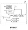
- FIG. 1 is a schematic representation of a mobile device 100 including an image sensor 110 in accordance with one embodiment of the invention.
- the mobile device 100 can be a cellular phone, a personal digital assistant (PDA), a video game console, a digital camera, a digital camcorder, a computing device, a wireless communication device, or another portable electronic device.
- the image sensor 110 is configured to selectively capture images of desired objects and provide current to recharge a battery in the mobile device 100.
- the illustrated mobile device 100 includes a signal processor 160, memory 170 electrically coupled to the signal processor 160, and a display 180 electrically coupled to the signal processor 160.
- the signal processor 160 is operably coupled to the image sensor 110 for processing signals generated by an array of pixels 120 on the image sensor 110. For example, when the image sensor 110 captures an image, the signal processor 160 can compress the signals (using image compression schemes such as JPEG, M-JPEG or MPEG) to reduce the data size and route the compressed signals to the memory 170. Moreover, the signal processor 160 can condition the signals from the image sensor 110 so that they are compatible with the display 180.
- the signal processor 160 can include one or more image encoders and decoders, memory, processor, microcontrollers, buffer, routers, timing circuitry, analog-to-digital converters, calibration circuitry, control circuitry, image processing circuitry (such as chromaticity), luminance signal processing circuitry, and/or other circuitry to process signals generated by the image sensor 110.
- the memory 170 can include volatile memory and/or non-volatile memory for storing signals from the signal processor 160.
- the display 180 can be attached, embedded, or otherwise native to the mobile device 100 to display signals from the signal processor 160.
- the display 180 can be one of a variety of display types suitable for mobile devices, such as liquid crystal display (LCD) or touchscreen.
- the display 180 can be a monochrome or color display.
- the mobile device 100 may also include a transceiver configured to transmit and receive wireless signals to and from another wireless device, and the signal processor 160 can compress and/or condition the signals for transmission to another device.
- the components of the mobile device 100 may be embodied as hardware, firmware, and/or software.
- the image sensor 110 and the signal processor 160 may comprise one chip, and the memory 170 may comprise yet another chip.
- the functionality of two or more chips may be embodied in a single chip such as a system-on-chip (SOC).
- SOC system-on-chip
- one or more components illustrated in Figure 1 may be omitted depending on the mobile device.
- more than one memory unit or a detachable or swappable memory unit may be included in the mobile device 100.
- the illustrated mobile device 100 further includes a battery 150 and a battery charger 152 both of which are contained within the housing of the device 100.
- the battery 150 powers the image sensor 110 and the other components of the device 100, and the battery charger 152 is operably coupled to the image sensor 110 to selectively charge the battery 150. More specifically, when the image sensor 110 is not capturing an image, the pixels 120 can provide signals or current to the battery charger 152 for charging the battery 150.
- the mobile device 100 includes a switch 140 movable between a first position (shown in Figure 1) and a second position (not shown).
- the switch 140 directs current from the image sensor 110 to the signal processor 160 so that the mobile device 100 can capture images.
- the switch 140 directs current from the image sensor 110 to the battery charger 152 for charging the battery 150.
- the switch 140 can be operably coupled to an actuatable switch (not shown) on the mobile device 100 that a user actuates to capture an image. In this case, the switch 140 moves from the second position to the first position when the user actuates the switch. After the image is captured, the switch 140 can move back to the second position.
- the image sensor 110 can be a single-chip color CMOS image sensor, such as those manufactured by Omnivision Technologies, Inc. of Sunnyvale, California, the assignee of the present invention.
- CMOS image sensors provide advantages over image sensors that use charge-coupled devices (CCDs), in that CCD image sensors have large sizes and power consumption that are not well suited for mobile devices.
- CCDs charge-coupled devices
- the image sensor can be a CCD.
- the illustrated image sensor 110 includes an array of pixels 120 and a timing/control circuit 130 operably coupled to the pixels 120.
- the timing/control circuit 130 operates the pixels 120 so that the pixels 120 produce signals either (a) in a sequence for the signal processor 160 to process, or (b) continuously and simultaneously for use in charging the battery 150.
- the timing/control circuit 130 can be operably coupled to the switch 140 and/or the actuatable switch discussed above so that the current from the pixels 120 is provided to the signal processor 160 or battery charger 152.
- Figure 2 is an enlarged schematic representation of the two-dimensional array of pixels 120 of Figure 1.
- the pixels 120 are arranged in columns 122 and rows 123, and although the illustrated embodiment includes seven columns 122 and four rows 123, other embodiments may include a different number of rows and columns.
- the individual pixels 120 are configured to convert incident light into an electrical signal, with the strength of the signal corresponding to the amount of light impinging on the pixel 120. These electrical signals can be used to charge the battery 150 ( Figure 1) or produce a digital image of the object reflecting light towards the pixels 120.
- the individual pixels 120 include a photodiode for generating an electrical signal and a transistor for controlling when the signal is output.
- Each pixel 120 in an individual column 122 outputs the electrical signal to a column signal line 124, which in turn transmits the signal to a column readout circuit 125.
- the column readout circuits 125 are shown at the "bottom" of Figure 2 for convenience purposes, the column readout circuits 125 can be placed almost anywhere on the integrated circuit relative to the array of pixels 120.
- the photodiodes when the image sensor 110 is used to capture an image of an object, the photodiodes generate electrical signals corresponding to the amount of light striking the pixels 120.
- the timing/control circuit 130 operates the pixels 120 so that the electrical signals of the pixels 120 are read out sequentially row-by-row. More specifically, one pixel 120 in each column 122 transmits its signal to the column readout circuit 125 at a single time. After the signals from one row 123 of pixels 120 are transmitted and read out at the column readout circuit 125, a subsequent row 123 of pixels 120 transmits signals to the column readout circuit 125. These signals are in turn transmitted from the column readout circuits 125 to the signal processor 160.
- the timing/control circuit 130 operates the pixels 120 so that the electrical signals from most, if not all, of the pixels 120 are transmitted simultaneously to the corresponding column readout circuits 125. Accordingly, more than one pixel 120 in each column 122 simultaneously transmits signals to the corresponding column readout circuit 125. Moreover, the pixels 120 continuously transmit signals to provide continuous current. The current from the pixels 120 is provided to the battery charger 152 to charge the battery 150.
- FIG. 3 is a flow diagram illustrating the operation of the mobile device 100 in accordance with one method of an invention.
- the user actuates a switch to capture an image of an object.
- the switch 140 moves to the first position and the pixels 120 provide signals sequentially row-by-row to the column readout circuits 125 and, in turn, to the signal processor 160.
- the signal processor 160 provides image data to the display 180 and/or the memory 170.
- the switch 140 moves from the first position to the second position and the pixels 120 simultaneously provide continuous current to the charger 152 for charging the battery 150.
- the image sensor 110 is configured to capture images and provide current to charge the battery 150. As such, the image sensor 110 can provide current from the pixels 120 to the battery charger 152 when the image sensor 110 is not capturing an image.
- An advantage of this feature is that the frequency with which the mobile device 100 must be plugged into an AC power outlet to recharge the battery 150 is reduced.
Landscapes
- Engineering & Computer Science (AREA)
- Multimedia (AREA)
- Signal Processing (AREA)
- Power Engineering (AREA)
- Charge And Discharge Circuits For Batteries Or The Like (AREA)
- Transforming Light Signals Into Electric Signals (AREA)
- Secondary Cells (AREA)
- Studio Devices (AREA)
Applications Claiming Priority (2)
| Application Number | Priority Date | Filing Date | Title |
|---|---|---|---|
| US10/808,655 US7405763B2 (en) | 2004-03-24 | 2004-03-24 | Mobile devices having an image sensor for charging a battery |
| US808655 | 2004-03-24 |
Publications (2)
| Publication Number | Publication Date |
|---|---|
| EP1580864A1 true EP1580864A1 (de) | 2005-09-28 |
| EP1580864B1 EP1580864B1 (de) | 2007-11-28 |
Family
ID=34862074
Family Applications (1)
| Application Number | Title | Priority Date | Filing Date |
|---|---|---|---|
| EP05251035A Expired - Lifetime EP1580864B1 (de) | 2004-03-24 | 2005-02-23 | Mobiles Gerät mit Bildsensoren zum Laden einer Batterie |
Country Status (6)
| Country | Link |
|---|---|
| US (2) | US7405763B2 (de) |
| EP (1) | EP1580864B1 (de) |
| CN (1) | CN100394640C (de) |
| AT (1) | ATE379868T1 (de) |
| DE (1) | DE602005003497T2 (de) |
| TW (1) | TWI305698B (de) |
Families Citing this family (15)
| Publication number | Priority date | Publication date | Assignee | Title |
|---|---|---|---|---|
| US7405763B2 (en) * | 2004-03-24 | 2008-07-29 | Omnivision Technologies, Inc. | Mobile devices having an image sensor for charging a battery |
| DE102008034279B4 (de) * | 2008-07-22 | 2012-04-26 | Fraunhofer-Gesellschaft zur Förderung der angewandten Forschung e.V. | Verfahren zum energieautarken Betrieb einer Vorrichtung sowie eine energieautarke Vorrichtung mit einem oder mehreren lichtempfindlichen Sensorelementen |
| US8629386B2 (en) * | 2009-02-27 | 2014-01-14 | The Hong Kong University Of Science And Technology | Method and apparatus for energy harvesting using CMOS sensor |
| KR101070612B1 (ko) * | 2009-09-29 | 2011-10-10 | 한국과학기술원 | 이미지 센서, 이의 동작 방법, 및 이를 포함하는 이미지 픽업 장치 |
| JP6174011B2 (ja) | 2011-05-12 | 2017-08-02 | デピュー シンセス プロダクツ, インコーポレーテッドDePuy Synthes Products, Inc. | 最小垂直相互接続を有するハイブリッド画像センサに対する積み重ねスキームを用いた画素アレイの領域最適化 |
| US9105538B2 (en) * | 2011-06-14 | 2015-08-11 | Moon J. Kim | Dynamically configurable photovoltaic cell array |
| TWI568134B (zh) * | 2011-10-24 | 2017-01-21 | 仁寶電腦工業股份有限公司 | 充電控制方法 |
| CN104486987A (zh) | 2012-07-26 | 2015-04-01 | 橄榄医疗公司 | 具有最小面积单片式cmos图像传感器的相机系统 |
| WO2014134501A2 (en) | 2013-02-28 | 2014-09-04 | Olive Medical Corporation | Videostroboscopy of vocal chords with cmos sensors |
| BR112015023206A2 (pt) | 2013-03-15 | 2017-08-22 | Olive Medical Corp | Sincronização de sensor de imagem sem temporizador de entrada e temporizador de transmissão de dados |
| JP6419774B2 (ja) | 2013-03-15 | 2018-11-07 | デピュイ・シンセス・プロダクツ・インコーポレイテッド | 内視鏡適用における画像センサi/o及びコンダクタ数の最少化 |
| WO2016112204A1 (en) | 2015-01-07 | 2016-07-14 | Nayar Shree K | Circuits for self-powered image sensors |
| US9407845B1 (en) * | 2015-03-26 | 2016-08-02 | Amazon Technologies, Inc. | Self powering camera |
| US10403656B2 (en) * | 2016-07-14 | 2019-09-03 | Purdue Research Foundation | Energy harvesting configurable image sensor |
| US11538847B2 (en) | 2018-02-23 | 2022-12-27 | The Regents Of The University Of Michigan | Imaging sensor and pixel structure for simultaneous imaging and energy harvesting |
Citations (5)
| Publication number | Priority date | Publication date | Assignee | Title |
|---|---|---|---|---|
| JPH0263330A (ja) * | 1988-08-30 | 1990-03-02 | Ricoh Co Ltd | 光電変換装置 |
| WO2000038415A1 (en) * | 1998-12-22 | 2000-06-29 | California Institute Of Technology | Highly miniaturized, battery operated, digital wireless camera |
| JP2003008958A (ja) * | 2001-06-21 | 2003-01-10 | Fuji Film Microdevices Co Ltd | 撮像装置 |
| EP1309178A2 (de) * | 2001-11-06 | 2003-05-07 | Omnivision Technologies Inc. | Signalausleseschaltung ohne Gleichstromverbrauch für einem CMOS Bildsensor |
| US6803553B1 (en) * | 2001-05-23 | 2004-10-12 | Pixim, Inc. | Image sensor with charge recycling |
Family Cites Families (18)
| Publication number | Priority date | Publication date | Assignee | Title |
|---|---|---|---|---|
| JPH026330A (ja) | 1988-03-07 | 1990-01-10 | Sanyo Electric Co Ltd | 超電導材料及び超電導体単結晶の製造方法 |
| GB9524483D0 (en) * | 1995-11-30 | 1996-01-31 | Philips Electronics Nv | Light sensing array device and apparatus incorporating such |
| US6721008B2 (en) * | 1998-01-22 | 2004-04-13 | Eastman Kodak Company | Integrated CMOS active pixel digital camera |
| JP2000050132A (ja) * | 1998-07-29 | 2000-02-18 | Fuji Photo Film Co Ltd | 電子カメラおよびその動作制御方法 |
| US6778212B1 (en) * | 2000-02-22 | 2004-08-17 | Pixim, Inc. | Digital image sensor with on -chip programmable logic |
| JP2002094873A (ja) * | 2000-09-14 | 2002-03-29 | Fuji Photo Film Co Ltd | デジタルカメラ |
| CA2351025A1 (en) * | 2001-06-19 | 2002-12-19 | Symagery Microsystems Inc. | Method and apparatus for controlling power consumption in an active pixel sensor array |
| US6914227B2 (en) * | 2001-06-25 | 2005-07-05 | Canon Kabushiki Kaisha | Image sensing apparatus capable of outputting image by converting resolution by adding and reading out a plurality of pixels, its control method, and image sensing system |
| JP3539414B2 (ja) * | 2001-09-25 | 2004-07-07 | 株式会社日立製作所 | 情報記録装置 |
| JP2003179820A (ja) * | 2001-12-11 | 2003-06-27 | Hitachi Ltd | Cmos型固体撮像素子を用いた撮像システムおよび撮像装置 |
| US7068319B2 (en) * | 2002-02-01 | 2006-06-27 | Micron Technology, Inc. | CMOS image sensor with a low-power architecture |
| US6730900B2 (en) * | 2002-02-05 | 2004-05-04 | E-Phocus, Inc. | Camera with MOS or CMOS sensor array |
| JP2004112422A (ja) * | 2002-09-19 | 2004-04-08 | Canon Inc | 撮像装置 |
| US7782377B2 (en) * | 2003-02-26 | 2010-08-24 | Canon Kabushiki Kaisha | Image sensing apparatus, control method therefor, storage medium, and program to create correction data |
| US20040257463A1 (en) * | 2003-06-17 | 2004-12-23 | Goris Andrew C. | User interface for digital camera having nonvolatile memory for storing intermediate data for advanced processing and capable of slowing, delaying and/or suspending advanced processing during low battery conditions |
| US7405763B2 (en) * | 2004-03-24 | 2008-07-29 | Omnivision Technologies, Inc. | Mobile devices having an image sensor for charging a battery |
| US7605398B2 (en) * | 2005-08-26 | 2009-10-20 | National Chung Cheng University | Apparatus of high dynamic-range CMOS image sensor and method thereof |
| US8629386B2 (en) * | 2009-02-27 | 2014-01-14 | The Hong Kong University Of Science And Technology | Method and apparatus for energy harvesting using CMOS sensor |
-
2004
- 2004-03-24 US US10/808,655 patent/US7405763B2/en active Active
-
2005
- 2005-02-04 TW TW094103710A patent/TWI305698B/zh not_active IP Right Cessation
- 2005-02-23 DE DE602005003497T patent/DE602005003497T2/de not_active Expired - Fee Related
- 2005-02-23 EP EP05251035A patent/EP1580864B1/de not_active Expired - Lifetime
- 2005-02-23 AT AT05251035T patent/ATE379868T1/de not_active IP Right Cessation
- 2005-03-23 CN CNB2005100601042A patent/CN100394640C/zh not_active Expired - Lifetime
-
2008
- 2008-05-27 US US12/127,158 patent/US7936394B2/en not_active Expired - Lifetime
Patent Citations (5)
| Publication number | Priority date | Publication date | Assignee | Title |
|---|---|---|---|---|
| JPH0263330A (ja) * | 1988-08-30 | 1990-03-02 | Ricoh Co Ltd | 光電変換装置 |
| WO2000038415A1 (en) * | 1998-12-22 | 2000-06-29 | California Institute Of Technology | Highly miniaturized, battery operated, digital wireless camera |
| US6803553B1 (en) * | 2001-05-23 | 2004-10-12 | Pixim, Inc. | Image sensor with charge recycling |
| JP2003008958A (ja) * | 2001-06-21 | 2003-01-10 | Fuji Film Microdevices Co Ltd | 撮像装置 |
| EP1309178A2 (de) * | 2001-11-06 | 2003-05-07 | Omnivision Technologies Inc. | Signalausleseschaltung ohne Gleichstromverbrauch für einem CMOS Bildsensor |
Non-Patent Citations (2)
| Title |
|---|
| PATENT ABSTRACTS OF JAPAN vol. 014, no. 239 (E - 0930) 21 May 1990 (1990-05-21) * |
| PATENT ABSTRACTS OF JAPAN vol. 2003, no. 05 12 May 2003 (2003-05-12) * |
Also Published As
| Publication number | Publication date |
|---|---|
| ATE379868T1 (de) | 2007-12-15 |
| US7405763B2 (en) | 2008-07-29 |
| TWI305698B (en) | 2009-01-21 |
| US7936394B2 (en) | 2011-05-03 |
| TW200601663A (en) | 2006-01-01 |
| DE602005003497D1 (de) | 2008-01-10 |
| DE602005003497T2 (de) | 2008-10-16 |
| EP1580864B1 (de) | 2007-11-28 |
| US20080225160A1 (en) | 2008-09-18 |
| US20050212957A1 (en) | 2005-09-29 |
| CN1674349A (zh) | 2005-09-28 |
| CN100394640C (zh) | 2008-06-11 |
Similar Documents
| Publication | Publication Date | Title |
|---|---|---|
| US7936394B2 (en) | Mobile devices having an image sensor for charging a battery | |
| US7286170B2 (en) | Solid-state image sensor, camera using the same, camera control system, and signal output device | |
| CN106341628B (zh) | 具有宽动态范围的图像传感器、像素电路和操作方法 | |
| US10529756B2 (en) | Imaging element and imaging apparatus | |
| CN102124566B (zh) | 用于3维合成像素的高增益读取电路 | |
| CN101193216B (zh) | 固态成像设备和成像装置 | |
| US10623673B2 (en) | Imaging device, imaging method, and imaging program | |
| US20130293753A1 (en) | Image data compression using stacked-chip image sensors | |
| KR20150020432A (ko) | 이미지 센서, 아날로그-디지털 컨버터 및 아날로그-디지털 변환 방법 | |
| CN108270981A (zh) | 像素单元及其成像方法和成像装置 | |
| KR20100095002A (ko) | 공유 처리되는 다중 이미지 센서 시스템 | |
| JP2008236620A (ja) | 固体撮像装置及び撮像装置 | |
| US12363446B2 (en) | Image sensor processing merged image and image processing system comprising the same | |
| CN113571538A (zh) | 像素结构、图像传感器、控制方法及装置、电子设备 | |
| US10306196B2 (en) | Pixel mixing device and method for controlling operation of same | |
| US20210021751A1 (en) | Image sensor and image processing system comprising the same | |
| US10075686B2 (en) | Color-image-data contamination correction device and imaging device, and method for controlling operation thereof | |
| JP2025147199A (ja) | 撮像素子及び撮像装置 | |
| US7019774B2 (en) | Imaging apparatus and mobile terminal incorporating same | |
| US9727948B2 (en) | Pixel interpolation device and operation control method | |
| WO2018055948A1 (ja) | 撮像装置、撮像装置の作動方法、撮像装置の作動プログラム | |
| JP2021044623A (ja) | 撮像装置及びその制御方法 | |
| US20050068435A1 (en) | Imaging device and imaging method | |
| US20170366771A1 (en) | Comparing circuit and an image sensor including a current stabilization circuit | |
| KR100827680B1 (ko) | 썸네일 데이터 전송 방법 및 장치 |
Legal Events
| Date | Code | Title | Description |
|---|---|---|---|
| PUAI | Public reference made under article 153(3) epc to a published international application that has entered the european phase |
Free format text: ORIGINAL CODE: 0009012 |
|
| AK | Designated contracting states |
Kind code of ref document: A1 Designated state(s): AT BE BG CH CY CZ DE DK EE ES FI FR GB GR HU IE IS IT LI LT LU MC NL PL PT RO SE SI SK TR |
|
| AX | Request for extension of the european patent |
Extension state: AL BA HR LV MK YU |
|
| 17P | Request for examination filed |
Effective date: 20051014 |
|
| AKX | Designation fees paid |
Designated state(s): AT BE BG CH CY CZ DE DK EE ES FI FR GB GR HU IE IS IT LI LT LU MC NL PL PT RO SE SI SK TR |
|
| GRAP | Despatch of communication of intention to grant a patent |
Free format text: ORIGINAL CODE: EPIDOSNIGR1 |
|
| GRAS | Grant fee paid |
Free format text: ORIGINAL CODE: EPIDOSNIGR3 |
|
| GRAA | (expected) grant |
Free format text: ORIGINAL CODE: 0009210 |
|
| AK | Designated contracting states |
Kind code of ref document: B1 Designated state(s): AT BE BG CH CY CZ DE DK EE ES FI FR GB GR HU IE IS IT LI LT LU MC NL PL PT RO SE SI SK TR |
|
| REG | Reference to a national code |
Ref country code: GB Ref legal event code: FG4D |
|
| REG | Reference to a national code |
Ref country code: IE Ref legal event code: FG4D |
|
| REG | Reference to a national code |
Ref country code: CH Ref legal event code: EP |
|
| REF | Corresponds to: |
Ref document number: 602005003497 Country of ref document: DE Date of ref document: 20080110 Kind code of ref document: P |
|
| PG25 | Lapsed in a contracting state [announced via postgrant information from national office to epo] |
Ref country code: ES Free format text: LAPSE BECAUSE OF FAILURE TO SUBMIT A TRANSLATION OF THE DESCRIPTION OR TO PAY THE FEE WITHIN THE PRESCRIBED TIME-LIMIT Effective date: 20080311 Ref country code: CH Free format text: LAPSE BECAUSE OF FAILURE TO SUBMIT A TRANSLATION OF THE DESCRIPTION OR TO PAY THE FEE WITHIN THE PRESCRIBED TIME-LIMIT Effective date: 20071128 Ref country code: SE Free format text: LAPSE BECAUSE OF FAILURE TO SUBMIT A TRANSLATION OF THE DESCRIPTION OR TO PAY THE FEE WITHIN THE PRESCRIBED TIME-LIMIT Effective date: 20080228 Ref country code: NL Free format text: LAPSE BECAUSE OF FAILURE TO SUBMIT A TRANSLATION OF THE DESCRIPTION OR TO PAY THE FEE WITHIN THE PRESCRIBED TIME-LIMIT Effective date: 20071128 Ref country code: LI Free format text: LAPSE BECAUSE OF FAILURE TO SUBMIT A TRANSLATION OF THE DESCRIPTION OR TO PAY THE FEE WITHIN THE PRESCRIBED TIME-LIMIT Effective date: 20071128 |
|
| NLV1 | Nl: lapsed or annulled due to failure to fulfill the requirements of art. 29p and 29m of the patents act | ||
| PG25 | Lapsed in a contracting state [announced via postgrant information from national office to epo] |
Ref country code: PL Free format text: LAPSE BECAUSE OF FAILURE TO SUBMIT A TRANSLATION OF THE DESCRIPTION OR TO PAY THE FEE WITHIN THE PRESCRIBED TIME-LIMIT Effective date: 20071128 Ref country code: BG Free format text: LAPSE BECAUSE OF FAILURE TO SUBMIT A TRANSLATION OF THE DESCRIPTION OR TO PAY THE FEE WITHIN THE PRESCRIBED TIME-LIMIT Effective date: 20080228 Ref country code: LT Free format text: LAPSE BECAUSE OF FAILURE TO SUBMIT A TRANSLATION OF THE DESCRIPTION OR TO PAY THE FEE WITHIN THE PRESCRIBED TIME-LIMIT Effective date: 20071128 Ref country code: FI Free format text: LAPSE BECAUSE OF FAILURE TO SUBMIT A TRANSLATION OF THE DESCRIPTION OR TO PAY THE FEE WITHIN THE PRESCRIBED TIME-LIMIT Effective date: 20071128 Ref country code: SI Free format text: LAPSE BECAUSE OF FAILURE TO SUBMIT A TRANSLATION OF THE DESCRIPTION OR TO PAY THE FEE WITHIN THE PRESCRIBED TIME-LIMIT Effective date: 20071128 Ref country code: IS Free format text: LAPSE BECAUSE OF FAILURE TO SUBMIT A TRANSLATION OF THE DESCRIPTION OR TO PAY THE FEE WITHIN THE PRESCRIBED TIME-LIMIT Effective date: 20080328 |
|
| PGFP | Annual fee paid to national office [announced via postgrant information from national office to epo] |
Ref country code: DE Payment date: 20080313 Year of fee payment: 4 |
|
| REG | Reference to a national code |
Ref country code: CH Ref legal event code: PL |
|
| PG25 | Lapsed in a contracting state [announced via postgrant information from national office to epo] |
Ref country code: AT Free format text: LAPSE BECAUSE OF FAILURE TO SUBMIT A TRANSLATION OF THE DESCRIPTION OR TO PAY THE FEE WITHIN THE PRESCRIBED TIME-LIMIT Effective date: 20071128 |
|
| ET | Fr: translation filed | ||
| PG25 | Lapsed in a contracting state [announced via postgrant information from national office to epo] |
Ref country code: CZ Free format text: LAPSE BECAUSE OF FAILURE TO SUBMIT A TRANSLATION OF THE DESCRIPTION OR TO PAY THE FEE WITHIN THE PRESCRIBED TIME-LIMIT Effective date: 20071128 Ref country code: DK Free format text: LAPSE BECAUSE OF FAILURE TO SUBMIT A TRANSLATION OF THE DESCRIPTION OR TO PAY THE FEE WITHIN THE PRESCRIBED TIME-LIMIT Effective date: 20071128 |
|
| PG25 | Lapsed in a contracting state [announced via postgrant information from national office to epo] |
Ref country code: SK Free format text: LAPSE BECAUSE OF FAILURE TO SUBMIT A TRANSLATION OF THE DESCRIPTION OR TO PAY THE FEE WITHIN THE PRESCRIBED TIME-LIMIT Effective date: 20071128 Ref country code: BE Free format text: LAPSE BECAUSE OF FAILURE TO SUBMIT A TRANSLATION OF THE DESCRIPTION OR TO PAY THE FEE WITHIN THE PRESCRIBED TIME-LIMIT Effective date: 20071128 Ref country code: RO Free format text: LAPSE BECAUSE OF FAILURE TO SUBMIT A TRANSLATION OF THE DESCRIPTION OR TO PAY THE FEE WITHIN THE PRESCRIBED TIME-LIMIT Effective date: 20071128 |
|
| PG25 | Lapsed in a contracting state [announced via postgrant information from national office to epo] |
Ref country code: PT Free format text: LAPSE BECAUSE OF FAILURE TO SUBMIT A TRANSLATION OF THE DESCRIPTION OR TO PAY THE FEE WITHIN THE PRESCRIBED TIME-LIMIT Effective date: 20080428 |
|
| PLBE | No opposition filed within time limit |
Free format text: ORIGINAL CODE: 0009261 |
|
| STAA | Information on the status of an ep patent application or granted ep patent |
Free format text: STATUS: NO OPPOSITION FILED WITHIN TIME LIMIT |
|
| PG25 | Lapsed in a contracting state [announced via postgrant information from national office to epo] |
Ref country code: MC Free format text: LAPSE BECAUSE OF NON-PAYMENT OF DUE FEES Effective date: 20080228 |
|
| PGFP | Annual fee paid to national office [announced via postgrant information from national office to epo] |
Ref country code: IE Payment date: 20080520 Year of fee payment: 4 |
|
| 26N | No opposition filed |
Effective date: 20080829 |
|
| PGFP | Annual fee paid to national office [announced via postgrant information from national office to epo] |
Ref country code: FR Payment date: 20080327 Year of fee payment: 4 |
|
| PG25 | Lapsed in a contracting state [announced via postgrant information from national office to epo] |
Ref country code: GR Free format text: LAPSE BECAUSE OF FAILURE TO SUBMIT A TRANSLATION OF THE DESCRIPTION OR TO PAY THE FEE WITHIN THE PRESCRIBED TIME-LIMIT Effective date: 20080229 Ref country code: EE Free format text: LAPSE BECAUSE OF FAILURE TO SUBMIT A TRANSLATION OF THE DESCRIPTION OR TO PAY THE FEE WITHIN THE PRESCRIBED TIME-LIMIT Effective date: 20071128 |
|
| PG25 | Lapsed in a contracting state [announced via postgrant information from national office to epo] |
Ref country code: CY Free format text: LAPSE BECAUSE OF FAILURE TO SUBMIT A TRANSLATION OF THE DESCRIPTION OR TO PAY THE FEE WITHIN THE PRESCRIBED TIME-LIMIT Effective date: 20071128 |
|
| GBPC | Gb: european patent ceased through non-payment of renewal fee |
Effective date: 20090223 |
|
| REG | Reference to a national code |
Ref country code: FR Ref legal event code: ST Effective date: 20091030 |
|
| PG25 | Lapsed in a contracting state [announced via postgrant information from national office to epo] |
Ref country code: DE Free format text: LAPSE BECAUSE OF NON-PAYMENT OF DUE FEES Effective date: 20090901 Ref country code: IE Free format text: LAPSE BECAUSE OF NON-PAYMENT OF DUE FEES Effective date: 20090223 |
|
| PG25 | Lapsed in a contracting state [announced via postgrant information from national office to epo] |
Ref country code: GB Free format text: LAPSE BECAUSE OF NON-PAYMENT OF DUE FEES Effective date: 20090223 Ref country code: FR Free format text: LAPSE BECAUSE OF NON-PAYMENT OF DUE FEES Effective date: 20090302 |
|
| PG25 | Lapsed in a contracting state [announced via postgrant information from national office to epo] |
Ref country code: HU Free format text: LAPSE BECAUSE OF FAILURE TO SUBMIT A TRANSLATION OF THE DESCRIPTION OR TO PAY THE FEE WITHIN THE PRESCRIBED TIME-LIMIT Effective date: 20080529 Ref country code: LU Free format text: LAPSE BECAUSE OF NON-PAYMENT OF DUE FEES Effective date: 20080223 |
|
| PG25 | Lapsed in a contracting state [announced via postgrant information from national office to epo] |
Ref country code: TR Free format text: LAPSE BECAUSE OF FAILURE TO SUBMIT A TRANSLATION OF THE DESCRIPTION OR TO PAY THE FEE WITHIN THE PRESCRIBED TIME-LIMIT Effective date: 20071128 |
|
| PG25 | Lapsed in a contracting state [announced via postgrant information from national office to epo] |
Ref country code: IT Free format text: LAPSE BECAUSE OF NON-PAYMENT OF DUE FEES Effective date: 20080229 |