EP1579528B1 - Transition entre un guide d onde rectangulaire et une ligne microruban - Google Patents
Transition entre un guide d onde rectangulaire et une ligne microruban Download PDFInfo
- Publication number
- EP1579528B1 EP1579528B1 EP03810852A EP03810852A EP1579528B1 EP 1579528 B1 EP1579528 B1 EP 1579528B1 EP 03810852 A EP03810852 A EP 03810852A EP 03810852 A EP03810852 A EP 03810852A EP 1579528 B1 EP1579528 B1 EP 1579528B1
- Authority
- EP
- European Patent Office
- Prior art keywords
- microstrip line
- waveguide
- substrate
- transition
- rib
- Prior art date
- Legal status (The legal status is an assumption and is not a legal conclusion. Google has not performed a legal analysis and makes no representation as to the accuracy of the status listed.)
- Expired - Lifetime
Links
- 230000007704 transition Effects 0.000 title claims description 28
- 239000000758 substrate Substances 0.000 claims description 29
- 239000006260 foam Substances 0.000 claims description 17
- 238000001465 metallisation Methods 0.000 claims description 7
- 229920002994 synthetic fiber Polymers 0.000 claims description 6
- 150000003949 imides Chemical class 0.000 claims description 3
- 229920000193 polymethacrylate Polymers 0.000 claims 1
- 238000004519 manufacturing process Methods 0.000 description 5
- 241000195940 Bryophyta Species 0.000 description 4
- 235000011929 mousse Nutrition 0.000 description 4
- 230000005540 biological transmission Effects 0.000 description 3
- 230000008859 change Effects 0.000 description 2
- 238000005516 engineering process Methods 0.000 description 2
- 238000003754 machining Methods 0.000 description 2
- 238000000034 method Methods 0.000 description 2
- 230000006978 adaptation Effects 0.000 description 1
- 230000003321 amplification Effects 0.000 description 1
- 230000000712 assembly Effects 0.000 description 1
- 238000000429 assembly Methods 0.000 description 1
- 230000015572 biosynthetic process Effects 0.000 description 1
- 230000001680 brushing effect Effects 0.000 description 1
- 230000015556 catabolic process Effects 0.000 description 1
- 210000004027 cell Anatomy 0.000 description 1
- 239000004020 conductor Substances 0.000 description 1
- 230000008878 coupling Effects 0.000 description 1
- 238000010168 coupling process Methods 0.000 description 1
- 238000005859 coupling reaction Methods 0.000 description 1
- 238000005520 cutting process Methods 0.000 description 1
- 238000006731 degradation reaction Methods 0.000 description 1
- 238000010586 diagram Methods 0.000 description 1
- 238000001914 filtration Methods 0.000 description 1
- 238000013012 foaming technology Methods 0.000 description 1
- 238000007731 hot pressing Methods 0.000 description 1
- 239000000463 material Substances 0.000 description 1
- 239000003607 modifier Substances 0.000 description 1
- 238000003199 nucleic acid amplification method Methods 0.000 description 1
- 239000002984 plastic foam Substances 0.000 description 1
- 229920007790 polymethacrylimide foam Polymers 0.000 description 1
- 230000008569 process Effects 0.000 description 1
- 230000009467 reduction Effects 0.000 description 1
- 238000003856 thermoforming Methods 0.000 description 1
Images
Classifications
-
- H—ELECTRICITY
- H01—ELECTRIC ELEMENTS
- H01P—WAVEGUIDES; RESONATORS, LINES, OR OTHER DEVICES OF THE WAVEGUIDE TYPE
- H01P5/00—Coupling devices of the waveguide type
- H01P5/08—Coupling devices of the waveguide type for linking dissimilar lines or devices
- H01P5/10—Coupling devices of the waveguide type for linking dissimilar lines or devices for coupling balanced lines or devices with unbalanced lines or devices
- H01P5/107—Hollow-waveguide/strip-line transitions
-
- H—ELECTRICITY
- H01—ELECTRIC ELEMENTS
- H01P—WAVEGUIDES; RESONATORS, LINES, OR OTHER DEVICES OF THE WAVEGUIDE TYPE
- H01P5/00—Coupling devices of the waveguide type
- H01P5/08—Coupling devices of the waveguide type for linking dissimilar lines or devices
-
- Y—GENERAL TAGGING OF NEW TECHNOLOGICAL DEVELOPMENTS; GENERAL TAGGING OF CROSS-SECTIONAL TECHNOLOGIES SPANNING OVER SEVERAL SECTIONS OF THE IPC; TECHNICAL SUBJECTS COVERED BY FORMER USPC CROSS-REFERENCE ART COLLECTIONS [XRACs] AND DIGESTS
- Y10—TECHNICAL SUBJECTS COVERED BY FORMER USPC
- Y10T—TECHNICAL SUBJECTS COVERED BY FORMER US CLASSIFICATION
- Y10T29/00—Metal working
- Y10T29/49—Method of mechanical manufacture
- Y10T29/49002—Electrical device making
- Y10T29/49016—Antenna or wave energy "plumbing" making
Definitions
- the invention relates to a transition between a rectangular waveguide and a microstrip line.
- the waveguide structures are often well suited for the realization of passive functions with low losses and high performance (antenna source such as corrugated cones, polarizers, filters, diplexers) more particularly at very high frequencies (centimetric bands and millimeter).
- the planar structures are on their side very well adapted for the low cost and large volume production of devices incorporating passive and active functions using conventional printed circuit manufacturing processes at frequencies up to the millimetric bands.
- the antenna source, the filter and the polarizer, if any are made in waveguide technology while the rest of the signal processing functions (weak amplification noise, mixing and intermediate filtering) are performed in conventional printed circuit technology.
- European Patent No. 0350324 discloses a transition between a waveguide structure and a microstrip transmission line in which a conductive line is supported within the waveguide perpendicularly to its axis and the microstrip transmission line. extends transversely across the wall of the waveguide in a position producing an energy coupling between the microstrip transmission line and the conductive line.
- a guided structure is formed on a microwave substrate.
- the rectangular waveguide is made by a double-sided metallization of the microwave substrate associated with metallized holes to make the lateral faces of the rectangular waveguide.
- the object of the invention is to propose a transition between a rectangular waveguide and a microstrip line that can be manufactured at low cost without assembling several parts.
- the transition is characterized in that it consists of a ribbed rectangular waveguide made in a bar of synthetic material whose metallized base under the rib is extended in the form of a plate of synthetic material constituting a substrate for the microstrip line, the rib having a bottom extending between the upper plane of the ribbed waveguide and the upper plane of the substrate and the microstrip line being disposed on the upper plane of the substrate in the extension of the bottom of the rib.
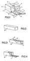
- FIG. 1 shows a block diagram of a transition according to the invention between a rectangular waveguide and a microstrip line.
- Figures 2 to 4 illustrate the process of manufacturing a transition according to the invention.
- a transition between a rectangular waveguide and a microstrip line is constituted by a ribbed rectangular waveguide G made in a plastic foam bar which also serves as a substrate for the microstrip line.
- the foam bar made of synthetic material, for example a polymethacryl imide foam known for its electrical characteristics close to those of air, for its mechanical characteristics of rigidity and lightness and for its weakness. cost, extends in a longitudinal direction A between two ends 1.2 between which is formed a shoulder 3 which extends perpendicular to the longitudinal direction A.
- This shoulder 3 defines an upper plane 4 of the ribbed waveguide and a top plane 5 of the substrate.
- the upper plane 5 of the substrate is offset perpendicularly to the longitudinal direction of the bar with a height H relative to the upper plane 4 of the ribbed waveguide, the height H corresponding to the height of the rib of the ribbed waveguide.
- the bottom of the rib 6 of the waveguide G extends between the upper plane 4 of the waveguide and the upper plane 5 of the substrate through the shoulder 3.
- the bottom and the lateral walls of the rib 6 are metallized, the metallization of the bottom of the rib 6 continuing on the upper plane 5 of the substrate to form the microstrip line 7.
- the metallized base 8 of the ribbed waveguide which extends under the rib 6 thus extends in the form of a foam plate constituting the substrate for the microstrip line.
- This metallized base thus serves as a ground plane for the microstrip line 7.
- the lateral faces 9 and 10 of the foam bar defining the ribbed rectangular waveguide are also metallized to the limit of the shoulder 3, although the metallization of the lateral flanks of the plate constituting the substrate of the microstrip line may not not degrade the electrical behavior of the microstrip line.
- the bottom of the rib 6, at the junction with the microstrip line 7, is at a distance E from the ground plane of the microstrip line, this distance E corresponding to the thickness of the substrate at the junction with the ribbed waveguide.
- the bottom of the rib 6 has a linear profile which allows to achieve simply by machining, stamping, hot pressing or cutting the foam bar.
- the rib 6 is centered in the width of the foam bar and its dimensions can be adjusted according to the desired working frequency range by ensuring an adequate stepwise transition from the quasi-TEM propagation mode of the microstrip line to the fundamental mode of the microstrip. guide. Such a gradual transition is made according to a given profile, linear, exponential or otherwise. And as a general rule, the minimum length of the profile obtained to ensure correct adaptation over the entire operating range must be of the order of a fraction of the wavelength (for example a quarter of the wavelength) corresponding to the lowest frequency.
- the microstrip line 7 may have a width identical to that of the rib or larger but it is well known that the width of a microstrip line depends on the thickness of the substrate on which it is arranged as well as its permittivity. Thus, it is possible to adjust the height of the substrate in the junction plane so as to obtain an identical width, or as close as possible to that of the rib. Then, to return to the thickness of the most suitable substrate, for the microstrip line 7, it is sufficient to gradually vary the thickness of the foam plate constituting the substrate in the longitudinal direction A.
- This thickness variation is made at quasi-constant characteristic impedance simultaneously modifying the width of the microstrip line which avoids passing through quarter-wave-type impedance transformers with discontinuous variation of line width which are at the origin of performance degradations ( losses, reduction of bandwidth).
- the impedance matching of the microstrip line is illustrated by a continuous linear decrease (represented in dashed line by 11) of the thickness of the substrate in the direction A and by a continuous linear decrease (represented as a line interrupted by 12) the width of the microstrip line over a certain length L of the microstrip line.
- Figures 2 to 4 illustrate a method of manufacturing the transition according to the invention in foam technology.
- a foam bar 20 is previously formed into a rectangular cross-sectional shape with dimensions that correspond to the inner dimensions of a rectangular waveguide for mono modal prior operation in the desired frequency range. Then, the foam bar is worked by machining, thermoforming, stamping or other to form the rib 6. The delimiting operation of the rib 6 in the section of the waveguide G can be extended at the section of the microstrip line 7.
- a complete metallization of the foam block 20 can then to be carried out, the metallization of the rib and the formation of the microstrip line being done simultaneously. Non-directive metallization by projection or brushing may be used.
- the foam block is cut transversely at the end of the rib 6 to form the plate-like substrate 5 of the microstrip line.
- the transition according to the invention is therefore carried out in one piece using a material of low permittivity, generating low losses and having good mechanical strength which contributes to obtaining a microstrip line whose dimensions are in agreement with those of the waveguide section. Furthermore, the realization of the transition according to the invention makes it possible to obtain an electrical and physical continuity between the waveguide and the microstrip line without the use of impedance transformers of the discontinuous change in line width type.
Landscapes
- Waveguides (AREA)
- Waveguide Aerials (AREA)
Description
- L'invention concerne une transition entre un guide d'onde rectangulaire' et une ligne microruban. Les structures en guide d'onde sont souvent bien adaptées pour la réalisation de fonctions passives à faibles pertes et à hautes performances (source d'antenne tels que cornets corrugués, polariseurs, filtres, diplexeurs) plus particulièrement aux très hautes fréquences (bandes centimétriques et millimétriques). Les structures planaires sont de leur côté très bien adaptées pour la production à bas coût et en grand volume de dispositifs intégrant des fonctions passives et actives utilisant les procédés de fabrication de circuits imprimés classiques à des fréquences pouvant aller jusqu'aux bandes millimétriques. Par exemple, dans une tête de réception satellite, assez souvent la source d'antenne, le filtre et le polariseur s'il y a lieu sont réalisés en technologie guide d'onde alors que le reste des fonctions de traitement du signal (amplification faible bruit, mélange et filtrages intermédiaires) sont réalisées en technologie circuit imprimé classique.
- Le brevet européen n°0350324 décrit une transition entre une structure guide d'onde et une ligne de transmission microruban selon laquelle une ligne conductrice est supportée à l'intérieur du guide d'onde de façon perpendiculaire à son axe et la ligne de transmission microruban s'étend transversalement à travers la paroi du guide d'onde dans une position produisant un couplage d'énergie entre la ligne de transmission microruban et la ligne conductrice.
- Le document IEEE -1995 - CESLT - page 1502 - « An improved approach to implement a microstrip to waveguide transition » - G. Zarba, G: Bertin, L. Accatino, P. Besso- décrit une transition entre un guide d'onde nervuré et une ligne microruban disposée sur un substrat. Dans la réalisation décrite, le substrat est glissé sous la partie nervurée du guide d'onde pour lui assurer une bonne stabilité mécanique et un assemblage aisé.
- Le document IEEEProceedings of APMC 2001, Taipei, Taiwan, ROC - page 543 - « A broadband Microstrip to Waveguide Transition using Planar Technique »- décrit une transition en bande Ka (26-40 GHz) qui est obtenue en insérant le substrat micro-onde, sur lequel est gravée une ligne microruban effilée, dans un guide d'onde rectangulaire partiellement rempli d'un diélectrique pour assurer une transition sans contact avec le conducteur chaud de la ligne microruban.
- Le document IEEE MICROWAVE AND WIRELESS COMPONENTS LETTERS, Vol 11, N°2, Février 2001 - page 68 - « Integrated Microstrip and Rectangular Waveguide in Planar Form » - Dominique Deslandes et Ke Wu - Cheg -Jung Lee, Hsien-Shun Wu & Ching-Kuang C. Tzuang - présente une version planaire d'une transition en bande ka (25-31 GHz). Une structure guidée est réalisée sur un substrat micro-onde. Le guide d'onde rectangulaire est réalisé par une métallisation double face du substrat micro-onde associée à des trous métallisés pour réaliser les faces latérales du guide d'onde rectangulaire.
- Le document US 6,265,950 B1 décrit un exemple de transition entre un guide d'onde rectangulaire et une ligne microruban ainsi que son procédé de fabrication.
- Ces réalisations d'une transition entre une structure en guide d'onde et une structure planaire s'avèrent relativement complexes à réaliser et requièrent des assemblages de plusieurs pièces qui doivent être d'autant plus précis que les fréquences de travail sont élevées. Par ailleurs, elles requièrent des substrats micro-onde de bonne qualité pour éviter les pertes diélectriques mais dont le coût est élevé.
- Le but de l'invention est de proposer une transition entre un guide d'onde rectangulaire et une ligne microruban qui peut être fabriquée à faible coût sans assemblage de plusieurs pièces.
- Selon l'invention, la transition est caractérisée en ce qu'elle consiste en un guide d'onde rectangulaire nervuré réalisé dans un barreau en matière synthétique dont la base métallisée sous la nervure se prolonge sous la forme d'une plaque en matière synthétique constituant un substrat pour la ligne microruban, la nervure ayant un fond s'étendant entre le plan supérieur du guide d'onde nervuré et le plan supérieur du substrat et la ligne microruban étant disposée sur le plan supérieur du substrat dans le prolongement du fond de la nervure.
- Selon des particularités de la transition selon l'invention :
- le fond de la nervure a un profil linéaire.
- la plaque en mousse constituant le substrat a une épaisseur qui varie selon une direction longitudinale pour modifier la largeur de la ligne microruban en maitenant son impédance caractéristique quasiment constante.
- la matiière synthétique est une mousse diélectrique présentant des caractéristiques électriques proches de celles de l'air, et
- la mousse est une mousse d'imide de polymétacrylate.
- D'autres caractéristiques et avantages de la transition selon l'invention apparaîtront encore mieux à la lecture de la description qui suit illustrée par les dessins.
- La figure 1 montre un schéma de principe d'une transition selon l'invention entre un guide d'onde rectangulaire et une ligne microruban.
- Les figures 2 à 4 illustrent le processus de fabrication d'une transition selon l'invention.
- Sur la figure 1, une transition entre un guide d'onde rectangulaire et une ligne microruban est constituée par un guide d'onde rectangulaire nervuré G réalisé dans un barreau de mousse en matière synthétique qui sert également de substrat pour la ligne microruban.
- Comme visible sur la figure 1, le barreau de mousse en matière synthétique, par exemple une mousse d'imide de polymétacrylate connu pour ses caractéristiques électriques proches de celles de l'air, pour ses caractéristiques mécaniques de rigidité et de légèreté et pour son faible coût de revient, s'étend selon une direction longitudinale A entre deux extrémités 1,2 entre lesquelles est formé un épaulement 3 qui s'étend perpendiculairement à la direction longitudinale A. Cet épaulement 3 définit un plan supérieur 4 du guide d'onde nervuré et un plan supérieur 5 du substrat. Le plan supérieur 5 du substrat est décalé perpendiculairement à la direction longitudinale du barreau d'une hauteur H par rapport au plan supérieur 4 du guide d'onde nervuré, la hauteur H correspondant à la hauteur de la nervure du guide d'onde nervuré.
- Le fond de la nervure 6 du guide d'onde G s'étend entre le plan supérieur 4 du guide d'onde et le plan supérieur 5 du substrat à travers l'épaulement 3. Le fond et les parois latérales de la nervure 6 sont métallisés, la métallisation du fond de la nervure 6 se poursuivant sur le plan supérieur 5 du substrat pour constituer la ligne microruban 7.
- La base métallisée 8 du guide d'onde nervuré qui s'étend sous la nervure 6 se prolonge donc sous la forme d'une plaque en mousse constituant le substrat pour la ligne microruban. Cette base métallisée sert donc de plan de masse pour la ligne microruban 7.
- Les faces latérales 9 et 10 du barreau de mousse définissant le guide d'onde rectangulaire nervuré sont également métallisées jusqu'à la limite de l'épaulement 3 bien que la métallisation des flancs latéraux de la plaque constituant le substrat de la ligne microruban puisse ne pas dégrader le comportement électrique de la ligne microruban.
- Comme visible sur la figure 1, le fond de la nervure 6, à la jonction avec la ligne microruban 7, est à une distance E du plan de masse de la ligne microruban, cette distance E correspondant à l'épaisseur du substrat à la jonction avec le guide d'onde nervuré.
- Sur la figure 1, le fond de la nervure 6 a un profil linéaire ce qui permet de la réaliser simplement par usinage, emboutissage, pressage à chaud ou par découpe du barreau de mousse.
- La nervure 6 est centrée dans la largeur du barreau de mousse et ses dimensions peuvent être ajustées en fonction de la plage de fréquence de travail souhaitée en assurant un passage progressif adequat du mode de propagation quasi-TEM de la ligne microruban vers le mode fondamental du guide. Un tel passage progressif, se fait selon un profil donné, linéaire, exponentiel ou autre. Et en règle générale, la longueur minimale du profil obtenu pour assurer une adaptation correcte sur toute la plage de fonctionnement doit être de l'ordre d'une fraction de la longueur d'onde (par exemple un quart de la longueur d'onde) correspondant à la fréquence la plus basse.
- A la jonction du fond de la nervure 6, la ligne microruban 7 peut avoir une largeur identique à celle de la nervure ou plus grande mais on sait bien que la largeur d'une ligne microruban dépend de l'épaisseur du substrat sur lequel elle est disposée ainsi que de sa permittivité. Ainsi, il est possible d'ajuster la hauteur du substrat dans le plan de jonction de manière à obtenir une largeur identique, ou la plus proche possible de celle de la nervure. Ensuite pour revenir à l'épaisseur de substrat la plus adaptée, pour la ligne microruban 7, il suffit de faire varier progressivement l'épaisseur de la plaque en mousse constituant le substrat selon la direction longitudinale A. Cette variation d'épaisseur se fait à impédance caractéristique quasi-constante en modifiant simultanément la largeur de la ligne microruban ce qui évite de passer par des transformateurs d'impédance de type quart-d'onde à variation discontinue de largeur de lignes qui sont à l'origine de dégradations de performances (pertes, réduction de la largeur de bande). Sur la figure 1, l'adaptation d'impédance de la ligne microruban est illustrée par une diminution continue linéaire (représentée en trait interrompu par 11) de l'épaisseur du substrat selon la direction A et par une diminution continue linéaire (représentée en trait interrompu par 12) de la largeur de la ligne microruban sur une certaine longueur L de la ligne microruban.
- Les figure 2 à 4 illustrent un mode de fabrication de la transition selon l'invention en technologie mousse. Un barreau de mousse 20 est préalablement mis sous une forme rectangulaire en section transversale avec des dimensions qui correspondent aux dimensions intérieures d'un guide d'onde rectangulaire pour un fonctionnement a priori mono modal dans la plage de fréquence souhaitée. Ensuite, le barreau de mousse est travaillé par usinage, thermoformage, emboutissage ou autre pour former la nervure 6. L'opération de délimitation de la nervure 6 dans la section du guide d'onde G peut être prolongée au niveau de la section de la ligne microruban 7. Une métallisation complète du bloc de mousse 20 peut ensuite être effectuée, la métallisation de la nervure et la formation de la ligne microruban se faisant de façon simultanée. On pourra utiliser une métallisation non directive par projection ou au pinceau. Ensuite, le bloc de mousse est découpé transversalement à l'extrémité de la nervure 6 pour former le substrat 5 en forme de plaque de la ligne microruban.
- La transition selon l'invention est donc réalisée en une seule pièce en utilisant un matériau de faible permittivité, engendrant de faibles pertes et ayant une bonne tenue mécanique ce qui contribue à l'obtention d'une ligne microruban dont les dimensions sont en accord avec celles de la section guide d'onde. Par ailleurs, la réalisation de la transition selon l'invention permet d'obtenir une continuité électrique et physique entre le guide d'onde et la ligne microruban sans recours à des transformateurs d'impédance de type changement discontinu de largeur de lignes.
Claims (5)
- Une transition entre un guide d onde rectangulaire et une ligne microruban, caractérisée en ce qu'elle consiste en un barreau (20) en matière synthétique comportant une première partie dont les faces latérales sont métallisées pour former un guide d'onde (G) et une deuxième partie prolongeant la première partie et formant un substrat pour une ligne microruban, ledit barreau présentant entre la partie formant guide d'onde et la partie formant substrat un épaulement (3) définissant un plan supérieur (4) de la partie formant guide d'onde et un plan supérieur (5) de la partie formant substrat, et comportant entre les deux plans supérieurs une nervure (6) ayant un fond et des parois métallisés ledit fond s'étendant entre les deux plans supérieurs, la métallisation du fond se prolongeant par la ligne microruban (7) réalisée sur le substrat, la base commune (8) à la première et à la deuxième parties étant entièrement métallisée.
- La transition selon la revendication 1, dans laquelle le fond de la nervure (6) a un profil linéaire.
- La transition selon la revendication 1 ou 2, dans laquelle la deuxième partie formant substrat a une épaisseur qui varie dans une direction prolongeant la première partie pour modifier la largeur de la ligne microruban (7) en maintenant son impédance caractéristique quasiment constante.
- La transition selon l'une des revendications 1 à 3, dans laquelle le matériau synthétique est une mousse diélectrique.
- La transition selon la revendication 4, dans laquelle la mousse diélectrique est une mousse d'imide de polymétacrylate.
Applications Claiming Priority (3)
| Application Number | Priority Date | Filing Date | Title |
|---|---|---|---|
| FR0300045 | 2003-01-03 | ||
| FR0300045A FR2849720B1 (fr) | 2003-01-03 | 2003-01-03 | Transition entre un guide d'onde rectangulaire et une ligne microruban |
| PCT/FR2003/050201 WO2004066432A1 (fr) | 2003-01-03 | 2003-12-22 | Transition entre un guide d'onde rectangulaire et une ligne microruban |
Publications (2)
| Publication Number | Publication Date |
|---|---|
| EP1579528A1 EP1579528A1 (fr) | 2005-09-28 |
| EP1579528B1 true EP1579528B1 (fr) | 2006-05-17 |
Family
ID=32524679
Family Applications (1)
| Application Number | Title | Priority Date | Filing Date |
|---|---|---|---|
| EP03810852A Expired - Lifetime EP1579528B1 (fr) | 2003-01-03 | 2003-12-22 | Transition entre un guide d onde rectangulaire et une ligne microruban |
Country Status (11)
| Country | Link |
|---|---|
| US (1) | US7382212B2 (fr) |
| EP (1) | EP1579528B1 (fr) |
| JP (1) | JP4263176B2 (fr) |
| KR (1) | KR100998207B1 (fr) |
| CN (1) | CN1322628C (fr) |
| AU (1) | AU2003302294A1 (fr) |
| BR (1) | BR0317729A (fr) |
| DE (1) | DE60305349T2 (fr) |
| FR (1) | FR2849720B1 (fr) |
| MX (1) | MXPA05007249A (fr) |
| WO (1) | WO2004066432A1 (fr) |
Families Citing this family (13)
| Publication number | Priority date | Publication date | Assignee | Title |
|---|---|---|---|---|
| US8305280B2 (en) * | 2009-11-04 | 2012-11-06 | Raytheon Company | Low loss broadband planar transmission line to waveguide transition |
| KR101902558B1 (ko) | 2010-07-02 | 2018-10-01 | 누보트로닉스, 인크. | 3차원 마이크로구조체 |
| US8552813B2 (en) | 2011-11-23 | 2013-10-08 | Raytheon Company | High frequency, high bandwidth, low loss microstrip to waveguide transition |
| US9065163B1 (en) | 2011-12-23 | 2015-06-23 | Nuvotronics, Llc | High frequency power combiner/divider |
| US9405064B2 (en) * | 2012-04-04 | 2016-08-02 | Texas Instruments Incorporated | Microstrip line of different widths, ground planes of different distances |
| US8952752B1 (en) | 2012-12-12 | 2015-02-10 | Nuvotronics, Llc | Smart power combiner |
| FR3010835B1 (fr) | 2013-09-19 | 2015-09-11 | Inst Mines Telecom Telecom Bretagne | Dispositif de jonction entre une ligne de transmission imprimee et un guide d'ondes dielectrique |
| DE102015221142A1 (de) | 2014-10-31 | 2016-05-19 | Anritsu Corporation | Übertragungsleitungs-Umwandlungsstruktur für ein Millimeterwellenband |
| CN106024921B (zh) * | 2016-06-30 | 2017-09-15 | 浙江大学 | 悬挂型可见光及近红外波段硅基光波导集成光电探测器 |
| CN106061093B (zh) * | 2016-08-04 | 2019-08-23 | 同方威视技术股份有限公司 | 用于电子直线加速器的波导系统以及电子直线加速器 |
| KR102674456B1 (ko) | 2017-01-26 | 2024-06-13 | 주식회사 케이엠더블유 | 전송선로-도파관 전이 장치 |
| US11664568B2 (en) * | 2019-06-11 | 2023-05-30 | Intel Corporation | Waveguides including at least one ridge associated with at least one dielectric core and the waveguides are surrounded by a conductive shell |
| JP2024064072A (ja) * | 2022-10-27 | 2024-05-14 | 古野電気株式会社 | 高周波回路、および、レーダ装置 |
Family Cites Families (8)
| Publication number | Priority date | Publication date | Assignee | Title |
|---|---|---|---|---|
| US2897461A (en) * | 1953-09-14 | 1959-07-28 | Boeing Co | Wave guide construction |
| US3265995A (en) * | 1964-03-18 | 1966-08-09 | Bell Telephone Labor Inc | Transmission line to waveguide junction |
| US3932823A (en) * | 1975-04-23 | 1976-01-13 | The United States Of America As Represented By The Secretary Of The Navy | Microstrip to waveguide adapter |
| JPH0435203A (ja) * | 1990-05-25 | 1992-02-06 | Sumitomo Electric Ind Ltd | マイクロ波デバイス |
| JPH05335816A (ja) * | 1992-06-03 | 1993-12-17 | Japan Radio Co Ltd | 導波管−マイクロストリップ線路変換器 |
| DE19636890C1 (de) * | 1996-09-11 | 1998-02-12 | Bosch Gmbh Robert | Übergang von einem Hohlleiter auf eine Streifenleitung |
| US6242984B1 (en) * | 1998-05-18 | 2001-06-05 | Trw Inc. | Monolithic 3D radial power combiner and splitter |
| DK1055264T3 (da) | 1998-12-10 | 2007-04-30 | Raytheon Co | Overgang fra bredbåndsmikrostrip til parallel-plade-bölgeleder |
-
2003
- 2003-01-03 FR FR0300045A patent/FR2849720B1/fr not_active Expired - Fee Related
- 2003-12-22 JP JP2004567029A patent/JP4263176B2/ja not_active Expired - Fee Related
- 2003-12-22 BR BR0317729-7A patent/BR0317729A/pt not_active IP Right Cessation
- 2003-12-22 CN CNB2003801081523A patent/CN1322628C/zh not_active Expired - Fee Related
- 2003-12-22 WO PCT/FR2003/050201 patent/WO2004066432A1/fr not_active Ceased
- 2003-12-22 KR KR1020057012057A patent/KR100998207B1/ko not_active Expired - Fee Related
- 2003-12-22 DE DE60305349T patent/DE60305349T2/de not_active Expired - Lifetime
- 2003-12-22 EP EP03810852A patent/EP1579528B1/fr not_active Expired - Lifetime
- 2003-12-22 AU AU2003302294A patent/AU2003302294A1/en not_active Abandoned
- 2003-12-22 MX MXPA05007249A patent/MXPA05007249A/es active IP Right Grant
- 2003-12-22 US US10/540,642 patent/US7382212B2/en not_active Expired - Lifetime
Also Published As
| Publication number | Publication date |
|---|---|
| KR100998207B1 (ko) | 2010-12-07 |
| AU2003302294A1 (en) | 2004-08-13 |
| CN1322628C (zh) | 2007-06-20 |
| BR0317729A (pt) | 2005-11-22 |
| FR2849720B1 (fr) | 2005-04-15 |
| FR2849720A1 (fr) | 2004-07-09 |
| US7382212B2 (en) | 2008-06-03 |
| MXPA05007249A (es) | 2005-09-08 |
| JP4263176B2 (ja) | 2009-05-13 |
| KR20050089078A (ko) | 2005-09-07 |
| DE60305349D1 (de) | 2006-06-22 |
| DE60305349T2 (de) | 2007-05-10 |
| CN1735995A (zh) | 2006-02-15 |
| WO2004066432A1 (fr) | 2004-08-05 |
| US20060152298A1 (en) | 2006-07-13 |
| JP2006513655A (ja) | 2006-04-20 |
| EP1579528A1 (fr) | 2005-09-28 |
Similar Documents
| Publication | Publication Date | Title |
|---|---|---|
| EP3840124B1 (fr) | Antenne à onde de fuite en technologie afsiw | |
| US20210399427A1 (en) | Self-filtering wideband millimeter wave antenna | |
| EP3843202B1 (fr) | Cornet pour antenne satellite bi-bande ka a polarisation circulaire | |
| EP2510574B1 (fr) | Dispositif de transition hyperfréquence entre une ligne à micro-ruban et un guide d'onde rectangulaire | |
| EP1433223B1 (fr) | Antenne fil-plaque multifrequences | |
| EP1579528A1 (fr) | Transition entre un guide d onde rectangulaire et une ligne microruban | |
| EP1576696A1 (fr) | Une antenne de faible volume notamment pour radiotelephones portatifs | |
| EP2643886B1 (fr) | Antenne planaire a bande passante elargie | |
| EP1751820B1 (fr) | Antenne planaire à plots conducteurs à partir du plan de masse et/ou d'au moins un élément rayonnant, et procédé de fabrication correspondant | |
| FR3095303A1 (fr) | Ecran polariseur a cellule(s) polarisante(s) radiofrequence(s) large bande | |
| Estrada et al. | A new broadband quasi Yagi–Uda antenna with an EBG-truncated ground plane | |
| FR2836286A1 (fr) | Accord dielectrique de faible cout de filtres plan e | |
| Abdel-Rahman | Design and development of high gain wideband microstrip antenna and DGS filters using numerical experimentation approach | |
| EP3047535B1 (fr) | Dispositif de jonction entre une ligne de transmission imprimée et un guide d'ondes diélectrique | |
| FR2866987A1 (fr) | Antenne planaire multibandes | |
| EP2409361A1 (fr) | Antenne a double ailettes | |
| Li et al. | Ultra-wideband printed elliptical slot antenna | |
| FR2853143A1 (fr) | Filtre flottant hyperfrequence en structure guide d'onde | |
| EP0991135A1 (fr) | Antenne sélective à commutation en fréquence | |
| FR2911998A1 (fr) | Antenne large bande | |
| FR2901062A1 (fr) | Dispositif rayonnant a cavite(s) resonnante(s) a air a fort rendement de surface, pour une antenne reseau | |
| Damaj | Versatile intricate antenna | |
| KR20020023740A (ko) | Nrd 가이드 회로 일체형 혼 안테나 | |
| FR3118836A1 (fr) | Dispositif d’antenne sur circuit imprimé et procédé de réalisation d’antenne(s) sur circuit(s) imprimé(s) | |
| EP0865097A1 (fr) | Procédé et dispositif de fabrication en guides d'ondes à fentes, notamment utilisables pour des longueurs d'ondes millimétriques |
Legal Events
| Date | Code | Title | Description |
|---|---|---|---|
| PUAI | Public reference made under article 153(3) epc to a published international application that has entered the european phase |
Free format text: ORIGINAL CODE: 0009012 |
|
| 17P | Request for examination filed |
Effective date: 20050624 |
|
| AK | Designated contracting states |
Kind code of ref document: A1 Designated state(s): AT BE BG CH CY CZ DE DK EE ES FI FR GB GR HU IE IT LI LU MC NL PT RO SE SI SK TR |
|
| AX | Request for extension of the european patent |
Extension state: AL LT LV MK |
|
| RAP1 | Party data changed (applicant data changed or rights of an application transferred) |
Owner name: THOMSON LICENSING |
|
| GRAP | Despatch of communication of intention to grant a patent |
Free format text: ORIGINAL CODE: EPIDOSNIGR1 |
|
| DAX | Request for extension of the european patent (deleted) | ||
| RBV | Designated contracting states (corrected) |
Designated state(s): DE FR GB IT |
|
| GRAS | Grant fee paid |
Free format text: ORIGINAL CODE: EPIDOSNIGR3 |
|
| GRAA | (expected) grant |
Free format text: ORIGINAL CODE: 0009210 |
|
| AK | Designated contracting states |
Kind code of ref document: B1 Designated state(s): DE FR GB IT |
|
| REG | Reference to a national code |
Ref country code: GB Ref legal event code: FG4D Free format text: NOT ENGLISH |
|
| REF | Corresponds to: |
Ref document number: 60305349 Country of ref document: DE Date of ref document: 20060622 Kind code of ref document: P |
|
| GBT | Gb: translation of ep patent filed (gb section 77(6)(a)/1977) |
Effective date: 20060706 |
|
| PLBE | No opposition filed within time limit |
Free format text: ORIGINAL CODE: 0009261 |
|
| STAA | Information on the status of an ep patent application or granted ep patent |
Free format text: STATUS: NO OPPOSITION FILED WITHIN TIME LIMIT |
|
| 26N | No opposition filed |
Effective date: 20070220 |
|
| PGFP | Annual fee paid to national office [announced via postgrant information from national office to epo] |
Ref country code: IT Payment date: 20101224 Year of fee payment: 8 |
|
| PG25 | Lapsed in a contracting state [announced via postgrant information from national office to epo] |
Ref country code: IT Free format text: LAPSE BECAUSE OF NON-PAYMENT OF DUE FEES Effective date: 20121222 |
|
| REG | Reference to a national code |
Ref country code: FR Ref legal event code: PLFP Year of fee payment: 13 |
|
| REG | Reference to a national code |
Ref country code: FR Ref legal event code: PLFP Year of fee payment: 14 |
|
| REG | Reference to a national code |
Ref country code: DE Ref legal event code: R082 Ref document number: 60305349 Country of ref document: DE Representative=s name: DEHNS, DE Ref country code: DE Ref legal event code: R082 Ref document number: 60305349 Country of ref document: DE Representative=s name: DEHNS PATENT AND TRADEMARK ATTORNEYS, DE Ref country code: DE Ref legal event code: R082 Ref document number: 60305349 Country of ref document: DE Representative=s name: HOFSTETTER, SCHURACK & PARTNER PATENT- UND REC, DE |
|
| REG | Reference to a national code |
Ref country code: FR Ref legal event code: PLFP Year of fee payment: 15 |
|
| REG | Reference to a national code |
Ref country code: FR Ref legal event code: TP Owner name: THOMSON LICENSING DTV, FR Effective date: 20180830 |
|
| REG | Reference to a national code |
Ref country code: GB Ref legal event code: 732E Free format text: REGISTERED BETWEEN 20180927 AND 20181005 |
|
| REG | Reference to a national code |
Ref country code: DE Ref legal event code: R082 Ref document number: 60305349 Country of ref document: DE Representative=s name: DEHNS, DE Ref country code: DE Ref legal event code: R081 Ref document number: 60305349 Country of ref document: DE Owner name: INTERDIGITAL MADISON PATENT HOLDINGS, FR Free format text: FORMER OWNER: THOMSON LICENSING, BOULOGNE BILLANCOURT, FR Ref country code: DE Ref legal event code: R082 Ref document number: 60305349 Country of ref document: DE Representative=s name: DEHNS PATENT AND TRADEMARK ATTORNEYS, DE |
|
| PGFP | Annual fee paid to national office [announced via postgrant information from national office to epo] |
Ref country code: FR Payment date: 20191224 Year of fee payment: 17 |
|
| PGFP | Annual fee paid to national office [announced via postgrant information from national office to epo] |
Ref country code: GB Payment date: 20191226 Year of fee payment: 17 Ref country code: DE Payment date: 20200131 Year of fee payment: 17 |
|
| REG | Reference to a national code |
Ref country code: DE Ref legal event code: R119 Ref document number: 60305349 Country of ref document: DE |
|
| GBPC | Gb: european patent ceased through non-payment of renewal fee |
Effective date: 20201222 |
|
| PG25 | Lapsed in a contracting state [announced via postgrant information from national office to epo] |
Ref country code: FR Free format text: LAPSE BECAUSE OF NON-PAYMENT OF DUE FEES Effective date: 20201231 |
|
| PG25 | Lapsed in a contracting state [announced via postgrant information from national office to epo] |
Ref country code: DE Free format text: LAPSE BECAUSE OF NON-PAYMENT OF DUE FEES Effective date: 20210701 Ref country code: GB Free format text: LAPSE BECAUSE OF NON-PAYMENT OF DUE FEES Effective date: 20201222 |