EP1579263B1 - Konfigurierbares beugendes optisches element - Google Patents
Konfigurierbares beugendes optisches element Download PDFInfo
- Publication number
- EP1579263B1 EP1579263B1 EP03781112A EP03781112A EP1579263B1 EP 1579263 B1 EP1579263 B1 EP 1579263B1 EP 03781112 A EP03781112 A EP 03781112A EP 03781112 A EP03781112 A EP 03781112A EP 1579263 B1 EP1579263 B1 EP 1579263B1
- Authority
- EP
- European Patent Office
- Prior art keywords
- sub
- elements
- grating
- diffractive
- optical
- Prior art date
- Legal status (The legal status is an assumption and is not a legal conclusion. Google has not performed a legal analysis and makes no representation as to the accuracy of the status listed.)
- Expired - Lifetime
Links
- 230000003287 optical effect Effects 0.000 title claims abstract description 38
- 230000003595 spectral effect Effects 0.000 claims abstract description 21
- 238000000034 method Methods 0.000 description 4
- 239000000758 substrate Substances 0.000 description 4
- 238000001914 filtration Methods 0.000 description 3
- 238000005459 micromachining Methods 0.000 description 3
- 238000004611 spectroscopical analysis Methods 0.000 description 3
- XUIMIQQOPSSXEZ-UHFFFAOYSA-N Silicon Chemical compound [Si] XUIMIQQOPSSXEZ-UHFFFAOYSA-N 0.000 description 2
- 238000013461 design Methods 0.000 description 2
- 238000005516 engineering process Methods 0.000 description 2
- 238000012545 processing Methods 0.000 description 2
- 229910052710 silicon Inorganic materials 0.000 description 2
- 239000010703 silicon Substances 0.000 description 2
- 238000001228 spectrum Methods 0.000 description 2
- 238000003491 array Methods 0.000 description 1
- 230000005540 biological transmission Effects 0.000 description 1
- 230000015572 biosynthetic process Effects 0.000 description 1
- 238000005100 correlation spectroscopy Methods 0.000 description 1
- 238000000354 decomposition reaction Methods 0.000 description 1
- 230000001934 delay Effects 0.000 description 1
- 230000001066 destructive effect Effects 0.000 description 1
- 238000001093 holography Methods 0.000 description 1
- 230000010365 information processing Effects 0.000 description 1
- 239000012212 insulator Substances 0.000 description 1
- 238000004519 manufacturing process Methods 0.000 description 1
- 239000011159 matrix material Substances 0.000 description 1
- 238000005259 measurement Methods 0.000 description 1
- 239000013307 optical fiber Substances 0.000 description 1
- 230000000737 periodic effect Effects 0.000 description 1
- 230000010363 phase shift Effects 0.000 description 1
- 229910021420 polycrystalline silicon Inorganic materials 0.000 description 1
- 229920005591 polysilicon Polymers 0.000 description 1
- 238000003786 synthesis reaction Methods 0.000 description 1
- 230000002194 synthesizing effect Effects 0.000 description 1
Images

Classifications
-
- G—PHYSICS
- G02—OPTICS
- G02B—OPTICAL ELEMENTS, SYSTEMS OR APPARATUS
- G02B5/00—Optical elements other than lenses
- G02B5/18—Diffraction gratings
- G02B5/1828—Diffraction gratings having means for producing variable diffraction
Definitions
- This invention relates to a configurable diffractive optical element comprising an array of diffractive sub-elements having a reflective surface.
- the decomposition of light into its component frequencies (wavelengths) is fundamental to optical spectroscopy.
- a class of optical devices is provided that serve as configurable spectral filters.
- the devices receive an incident beam composed of light of different frequencies. They direct part of the light in a certain direction or onto a focal point.
- the devices consist of a system of movable diffractive microstructures on a substrate. By applying different voltages to the device, we alter the relative positions of the microstructures and thus we also alter the spectral composition of the diffracted light.
- Spectral filters are important for all kinds of optical measurements.
- spectral filter in a broad sense to describe all devices that selectively remove light with specific frequencies, totally or partially, from a lightpath. If the properties of the filter can be changed over time by applying different voltages, temperatures or other means of actuation we call it a tunable or configurable filter.
- tunable and configurable filter There is no clear distinction between tunable and configurable except that the latter implies that a larger range of possible filter functions can be realized.
- Configurable optical filters are particularly important for spectroscopy.
- One example is the tiltable grating of a conventional monochromator. By our definitions this is an example of a tunable (or configurable) optical filter.
- a diffractive optical element is a generalized 1- or 2-dimensional optical grating or hologram, made to synthesize a light field by exposing different parts of an incident light beam to different phase delays and/or amplitude modulations.
- MEMS micro-electromechanical systems
- With current silicon micromachining technology it is not difficult to make moving parts with dimensions less than 10 micrometer.
- a configurable DOE CDOE
- the top of such moving parts will be an optical surface: Mirrors, gratings or more complex structures for filtering or focusing.
- each surface a diffractive sub-element. Their relative positions can be tuned with a resolution much less than typical optical wavelengths, and the interference between reflections from the different parts determines the resulting light field.
- the Polychromator A CDOE for synthesizing spectral filters
- the Polychromator has been designed and implemented by G.B. Hocker et al. "The polychromator: A programmable mems diffraction grating for synthetic spectra.” In Solid-State Sensor and Actuator Workshop, pages 89-91, Hilton Head Island, South Carolina, June 2000 .
- This device is an electrostatically controlled array of beams. The beams can move vertically and the top of each beam is reflecting and plays the role as a grating element.
- the underlying theory of synthetic filters is given by Michael B. Sinclair et al.
- optical apparatus for forming correlation spectrometers and optical processors.
- the optical apparatus comprises one or more diffractive optical elements formed on a substrate for receiving light from a source and processing the incident light.
- the optical apparatus includes an addressing element for alternately addressing each diffractive optical element thereof to produce for one unit of time a first correlation with the incident light, and to produce for a different unit of time a second correlation with the incident light that is different from the first correlation.
- the optical apparatus is in the form of a correlation spectrometer; and in other embodiments, the apparatus is in the form of an optical processor.
- the optical apparatus comprises a plurality of diffractive optical elements on a common substrate for forming first and second gratings that alternately intercept the incident light for different units of time.
- the optical apparatus includes an electrically-programmable diffraction grating that may be alternately switched between a plurality of grating states thereof for processing the incident light.
- the optical apparatus may be formed, at least in part, by a micromachining process.
- Electrically-programmable diffraction grating describes an electrically-programmable diffraction grating.
- the programmable grating includes a substrate having a plurality of electrodes formed thereon and a moveable grating element above each of the electrodes.
- the grating elements are electrostatically programmable to form a diffraction grating for diffracting an incident beam of light as it is reflected from the upper surfaces of the grating elements.
- the programmable diffraction grating formed by a micromachining process, has applications for optical information processing (e.g. optical correlators and computers), for multiplexing and demultiplexing a plurality of light beams of different wavelengths (e.g. for optical fiber communications), and for forming spectrometers (e.g. correlation and scanning spectrometers).
- a device of this type has the disadvantage of having to control a large number of elements to achieve high spectral resolution within a narrow spectral range.
- the invention also provides focusing of the light beam, eliminating the need for additional optical components.
- Fig. 1 which illustrates the known art
- p ( x ) rect ( x / d ).
- the highest optical frequency that can be resolved is proportional to Nd, the product of the number of grating elements and the grating period, while the cutoff frequency or free spectral range is given by the first zero of the sinc envelope function:
- Fig 2 illustrates a grating array according to an example wherein the flat top of the beams according to the known art described above is replaced with a short grating with a grating period d s . ⁇ d.
- p ( x ) rect ( x / d ) exp ( i 2 ⁇ x / d s ).
- P ( k x ) sinc ( k x d / 2 ⁇ -d / d s ).
- This is essentially a shifting of the sinc envelope of Eq 5 to the frequency of our choice.
- the frequency shift is determined by the ratio between the two grating periods.
- MEMS devices are based on SOI structures with lateral movement actuated by electrostatic comb drives. These structures are stiffer and also easier to fabricate than the multilayer polysilicon process often used to make beam structures with vertical movement.
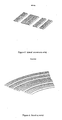
- Fig. 4 illustrates a focusing device according to an example. Extending to sub-elements with arbitrary shapes, it is possible to make focusing configurable spectral filters. If we shape the sub-elements as Fresnel Zones corresponding to a given focal length, it can be shown that the intensity in the focus is the same as for a one-dimensional beam array or array of gratings.
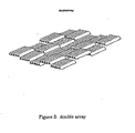
- Fig. 5 illustrates a double array according to an example providing a two-dimensional matrix of mirror elements, each comprising a diffractive grating at the surface.
- each sub-element is provided with a grating.
- the grating on each sub-element may be provided with any suitable grating period without other limitations than the ones present in the production of ordinary gratings.
- the dimensions of the diffractive sub-elements according to the invention preferably should correspond to a number of periods for the gratings on each sub-elements, e.g. in the order of 100 ⁇ m.
- the beams or sub-elements according to figures 2 , 4 and 5 may be moved in a directions perpendicular to the element surface. In figure 3 , however, as described above, the positions of the sub-elements may be shifted in the lateral direction parallel to the surface. Any combinations of these movements are of course possible, although more complicated to obtain in practice. Typically the movement relative to direction of the incoming or reflected light should be in the order of 1 ⁇ 2 the wavelength of the light.
Landscapes
- Physics & Mathematics (AREA)
- General Physics & Mathematics (AREA)
- Optics & Photonics (AREA)
- Mechanical Light Control Or Optical Switches (AREA)
- Diffracting Gratings Or Hologram Optical Elements (AREA)
- Prostheses (AREA)
- Optical Couplings Of Light Guides (AREA)
- Eyeglasses (AREA)
- Glass Compositions (AREA)
- Light Guides In General And Applications Therefor (AREA)
Claims (3)
- Einstellbares beugendes optisches Element, umfassend eine Anordnung aus rechteckigen beugenden Subelementen gleicher Größe, welche jeweils eine reflektierende Oberfläche aufweisen, wobei jedes Subelement angepasst ist, um in der Vertikalrichtung bezüglich der Oberfläche des Elements steuerbar bewegt zu werden, und wobei eine Anzahl der Subelemente mit einem Reflexionsbeugungsgitter mit einer Anzahl von ausgewählten Spektralcharakteristiken versehen ist,
dadurch gekennzeichnet, dass das Gitter an der Anzahl von Subelementen ein eine Beugungslinse bildendes fokussierendes beugendes Muster ist. - Beugendes optisches Element nach Anspruch 1, wobei die physikalische Größe des Subelements wesentlich größer ist als die typische räumliche Periode des Beugungsgitters an den Subelementen.
- Beugendes optisches Element nach Anspruch 1, wobei die Anordnung von Subelementen eine zweidimensionale Anordnung ist.
Applications Claiming Priority (3)
| Application Number | Priority Date | Filing Date | Title |
|---|---|---|---|
| NO20026279 | 2002-12-30 | ||
| NO20026279A NO318360B1 (no) | 2002-12-30 | 2002-12-30 | Konfigurerbart diffraktiv optisk element |
| PCT/NO2003/000437 WO2004059365A1 (en) | 2002-12-30 | 2003-12-22 | Configurable diffractive optical element |
Publications (2)
| Publication Number | Publication Date |
|---|---|
| EP1579263A1 EP1579263A1 (de) | 2005-09-28 |
| EP1579263B1 true EP1579263B1 (de) | 2010-12-01 |
Family
ID=19914344
Family Applications (1)
| Application Number | Title | Priority Date | Filing Date |
|---|---|---|---|
| EP03781112A Expired - Lifetime EP1579263B1 (de) | 2002-12-30 | 2003-12-22 | Konfigurierbares beugendes optisches element |
Country Status (14)
| Country | Link |
|---|---|
| US (2) | US7286292B2 (de) |
| EP (1) | EP1579263B1 (de) |
| JP (1) | JP5294532B2 (de) |
| CN (1) | CN100380171C (de) |
| AT (1) | ATE490486T1 (de) |
| AU (1) | AU2003288806A1 (de) |
| CA (1) | CA2511398C (de) |
| DE (1) | DE60335211D1 (de) |
| DK (1) | DK1579263T3 (de) |
| ES (1) | ES2357348T3 (de) |
| IL (1) | IL168578A (de) |
| NO (1) | NO318360B1 (de) |
| PT (1) | PT1579263E (de) |
| WO (1) | WO2004059365A1 (de) |
Families Citing this family (12)
| Publication number | Priority date | Publication date | Assignee | Title |
|---|---|---|---|---|
| US7420737B2 (en) * | 2005-12-21 | 2008-09-02 | Intel Corporation | Reconfigurable zone plate lens |
| DE102007047010B4 (de) * | 2007-10-01 | 2010-05-12 | Fraunhofer-Gesellschaft zur Förderung der angewandten Forschung e.V. | Mikromechanisches Bauelement zur Modulation von elektromagnetischer Strahlung und optisches System mit demselben |
| DE102007051520B4 (de) * | 2007-10-19 | 2021-01-14 | Seereal Technologies S.A. | Komplexwertiger räumlicher Lichtmodulator, räumliche Lichtmodulationseinrichtung und Verfahren zur Modulation eines Wellenfeldes |
| NO333724B1 (no) | 2009-08-14 | 2013-09-02 | Sintef | En mikromekanisk rekke med optisk reflekterende overflater |
| US8072684B2 (en) * | 2010-01-25 | 2011-12-06 | Toyota Motor Engineering & Manufacturing North America, Inc. | Optical device using laterally-shiftable diffraction gratings |
| GB2497295A (en) | 2011-12-05 | 2013-06-12 | Gassecure As | Method and system for gas detection |
| DE102012219655B4 (de) * | 2012-10-26 | 2018-10-25 | Albert-Ludwigs-Universität Freiburg | Optisches element und herstellung desselben |
| DE102017211910A1 (de) * | 2017-07-12 | 2019-01-17 | Dr. Johannes Heidenhain Gmbh | Diffraktiver Biosensor |
| TWI655457B (zh) * | 2017-10-27 | 2019-04-01 | National Taiwan University Of Science And Technology | 寬通頻帶光柵濾波器結構及其運作方法 |
| CN108802881B (zh) * | 2018-05-21 | 2022-03-08 | 苏州大学 | 一种高衍射效率光栅结构和制备方法 |
| US11675114B2 (en) * | 2018-07-23 | 2023-06-13 | Ii-Vi Delaware, Inc. | Monolithic structured light projector |
| GB201820293D0 (en) | 2018-12-13 | 2019-01-30 | Draeger Safety Ag & Co Kgaa | Gas sensor |
Citations (6)
| Publication number | Priority date | Publication date | Assignee | Title |
|---|---|---|---|---|
| US5757536A (en) * | 1995-08-30 | 1998-05-26 | Sandia Corporation | Electrically-programmable diffraction grating |
| US6172796B1 (en) * | 1998-12-18 | 2001-01-09 | Eastman Kodak Company | Multilevel electro-mechanical grating device and a method for operating a multilevel mechanical and electro-mechanical grating device |
| US6381061B2 (en) * | 1999-11-19 | 2002-04-30 | Nokia Corporation | Pixel structure having deformable material and method for forming a light valve |
| US20020105725A1 (en) * | 2000-12-18 | 2002-08-08 | Sweatt William C. | Electrically-programmable optical processor with enhanced resolution |
| US20020113860A1 (en) * | 2000-12-21 | 2002-08-22 | Eastman Kodak Company | Electromechanical grating display system with segmented waveplate |
| US20020195418A1 (en) * | 2000-01-26 | 2002-12-26 | Eastman Kodak Company | Method for manufacturing a mechanical conformal grating device with improved contrast and lifetime |
Family Cites Families (19)
| Publication number | Priority date | Publication date | Assignee | Title |
|---|---|---|---|---|
| US4729658A (en) * | 1986-06-05 | 1988-03-08 | The Perkin-Elmer Corporation | Very wide spectral coverage grating spectrometer |
| US5701005A (en) * | 1995-06-19 | 1997-12-23 | Eastman Kodak Company | Color separating diffractive optical array and image sensor |
| US5774254A (en) * | 1997-06-26 | 1998-06-30 | Xerox Corporation | Fault tolerant light modulator display system |
| KR100294540B1 (ko) | 1997-12-31 | 2001-07-12 | 윤종용 | 가변형처핑격자 |
| JP2000221313A (ja) * | 1999-01-29 | 2000-08-11 | Minolta Co Ltd | 動的回折素子 |
| JP4473975B2 (ja) * | 1999-04-16 | 2010-06-02 | キヤノン株式会社 | エンコーダ |
| JP3893809B2 (ja) * | 1999-09-29 | 2007-03-14 | コニカミノルタフォトイメージング株式会社 | 焦点位置を変更できる空間変調ユニット、光束偏向装置、焦点検出装置、およびカメラ |
| CA2352729A1 (en) | 2000-07-13 | 2002-01-13 | Creoscitex Corporation Ltd. | Blazed micro-mechanical light modulator and array thereof |
| JP2002074727A (ja) * | 2000-09-01 | 2002-03-15 | Samsung Electro Mech Co Ltd | ダイナミック制御回折格子並びに情報記録再生装置と情報再生装置 |
| JP2002122809A (ja) * | 2000-10-18 | 2002-04-26 | Canon Inc | 投射型表示装置 |
| US20020097508A1 (en) * | 2001-01-24 | 2002-07-25 | Konica Corporation | Objective lens for use in optical pickup apparatus and optical pickup apparatus |
| JP4437376B2 (ja) * | 2001-03-27 | 2010-03-24 | 株式会社リコー | 面発光レーザ素子の製造方法 |
| US6829092B2 (en) | 2001-08-15 | 2004-12-07 | Silicon Light Machines, Inc. | Blazed grating light valve |
| US6639722B2 (en) | 2001-08-15 | 2003-10-28 | Silicon Light Machines | Stress tuned blazed grating light valve |
| US7046410B2 (en) * | 2001-10-11 | 2006-05-16 | Polychromix, Inc. | Actuatable diffractive optical processor |
| US6959132B2 (en) * | 2002-03-13 | 2005-10-25 | Pts Corporation | One-to-M wavelength routing element |
| US20040218172A1 (en) * | 2003-01-24 | 2004-11-04 | Deverse Richard A. | Application of spatial light modulators for new modalities in spectrometry and imaging |
| KR100619335B1 (ko) * | 2004-06-03 | 2006-09-12 | 삼성전기주식회사 | 근접장을 이용한 광변조기 |
| US20060132766A1 (en) * | 2004-12-21 | 2006-06-22 | Bruce Richman | Continuously tunable external cavity diode laser |
-
2002
- 2002-12-30 NO NO20026279A patent/NO318360B1/no not_active IP Right Cessation
-
2003
- 2003-12-22 US US10/541,317 patent/US7286292B2/en not_active Expired - Lifetime
- 2003-12-22 AU AU2003288806A patent/AU2003288806A1/en not_active Abandoned
- 2003-12-22 WO PCT/NO2003/000437 patent/WO2004059365A1/en not_active Ceased
- 2003-12-22 JP JP2004563061A patent/JP5294532B2/ja not_active Expired - Lifetime
- 2003-12-22 PT PT03781112T patent/PT1579263E/pt unknown
- 2003-12-22 DE DE60335211T patent/DE60335211D1/de not_active Expired - Lifetime
- 2003-12-22 EP EP03781112A patent/EP1579263B1/de not_active Expired - Lifetime
- 2003-12-22 CN CNB2003801079538A patent/CN100380171C/zh not_active Expired - Lifetime
- 2003-12-22 DK DK03781112.2T patent/DK1579263T3/da active
- 2003-12-22 AT AT03781112T patent/ATE490486T1/de active
- 2003-12-22 CA CA2511398A patent/CA2511398C/en not_active Expired - Lifetime
- 2003-12-22 ES ES03781112T patent/ES2357348T3/es not_active Expired - Lifetime
-
2005
- 2005-05-15 IL IL168578A patent/IL168578A/en not_active IP Right Cessation
-
2007
- 2007-09-19 US US11/857,605 patent/US7463420B2/en not_active Expired - Lifetime
Patent Citations (6)
| Publication number | Priority date | Publication date | Assignee | Title |
|---|---|---|---|---|
| US5757536A (en) * | 1995-08-30 | 1998-05-26 | Sandia Corporation | Electrically-programmable diffraction grating |
| US6172796B1 (en) * | 1998-12-18 | 2001-01-09 | Eastman Kodak Company | Multilevel electro-mechanical grating device and a method for operating a multilevel mechanical and electro-mechanical grating device |
| US6381061B2 (en) * | 1999-11-19 | 2002-04-30 | Nokia Corporation | Pixel structure having deformable material and method for forming a light valve |
| US20020195418A1 (en) * | 2000-01-26 | 2002-12-26 | Eastman Kodak Company | Method for manufacturing a mechanical conformal grating device with improved contrast and lifetime |
| US20020105725A1 (en) * | 2000-12-18 | 2002-08-08 | Sweatt William C. | Electrically-programmable optical processor with enhanced resolution |
| US20020113860A1 (en) * | 2000-12-21 | 2002-08-22 | Eastman Kodak Company | Electromechanical grating display system with segmented waveplate |
Non-Patent Citations (3)
| Title |
|---|
| KOWARZ M.W.; BRAZAS J.C.; PHALEN J.G.: "Conformal grating electromechanical system (GEMS) for high-speed digital light modulation", PROCEEDINGS OF THE IEEE 15TH. ANNUAL INTERNATIONAL CONFERENCE ON MICRO ELECTRO MECHANICAL SYSTEMS, vol. CONF.15, 1 January 2002 (2002-01-01), NEW YORK, NY : IEEE, US, pages 568 - 573, XP010577719 * |
| PAPE D.R.; HORNBECK L.J.: "CHARACTERISTICS OF THE DEFORMABLE MIRROR DEVICE FOR OPTICAL INFORMATION PROCESSING", OPTICAL ENGINEERING, vol. 22, no. 6, 1 November 1983 (1983-11-01), SOC. OF PHOTO-OPTICAL INSTRUMENTATION ENGINEERS. BELLINGHAM, pages 675 - 681, XP000955412 * |
| SWANSON G.J.: "Binary Optics Technology: Theoretical Limits on the Diffraction Efficiency of Multi-level Diffractive Optical Elements", TECHNICAL REPORT. MASSACHUSETTS INSTITUTE OF TECHNOLOGYLINCOLN LABORATORY, no. 914, 1 March 1991 (1991-03-01), pages COMPLETE 32, XP002102141 * |
Also Published As
| Publication number | Publication date |
|---|---|
| CN1732402A (zh) | 2006-02-08 |
| NO20026279D0 (no) | 2002-12-30 |
| IL168578A (en) | 2012-06-28 |
| AU2003288806A1 (en) | 2004-07-22 |
| ATE490486T1 (de) | 2010-12-15 |
| US7286292B2 (en) | 2007-10-23 |
| CA2511398C (en) | 2010-04-13 |
| ES2357348T3 (es) | 2011-04-25 |
| US7463420B2 (en) | 2008-12-09 |
| EP1579263A1 (de) | 2005-09-28 |
| US20080007833A1 (en) | 2008-01-10 |
| DK1579263T3 (da) | 2011-01-31 |
| PT1579263E (pt) | 2011-02-02 |
| NO318360B1 (no) | 2005-03-07 |
| CN100380171C (zh) | 2008-04-09 |
| CA2511398A1 (en) | 2004-07-15 |
| WO2004059365A1 (en) | 2004-07-15 |
| US20060103936A1 (en) | 2006-05-18 |
| JP2006512602A (ja) | 2006-04-13 |
| JP5294532B2 (ja) | 2013-09-18 |
| DE60335211D1 (de) | 2011-01-13 |
Similar Documents
| Publication | Publication Date | Title |
|---|---|---|
| US7463420B2 (en) | Configurable diffractive optical element | |
| TWI410698B (zh) | Space light modifiers with regular permutations of pixels | |
| Wang et al. | 2D broadband beamsteering with large-scale MEMS optical phased array | |
| US5477383A (en) | Optical array method and apparatus | |
| US6804429B2 (en) | Reconfigurable wavelength multiplexers and filters employing micromirror array in a gires-tournois interferometer | |
| US6903872B2 (en) | Electrically reconfigurable optical devices | |
| EP2174168B1 (de) | Optische anordnung mit einem paar beugender optischer elemente | |
| CA2352729A1 (en) | Blazed micro-mechanical light modulator and array thereof | |
| KR20090022596A (ko) | 회절형 광변조기 및 이를 포함하는 디스플레이 장치 | |
| WO2004031867A2 (en) | System and method for holographic fabrication and replication of diffractive optical elements for maskless lithography | |
| US20060017999A1 (en) | Diffraction-based pulse shaping with a 2D optical modulator | |
| US6480333B1 (en) | Diffractive optical elements on non-flat substrates using electron beam lithography | |
| Sagberg et al. | Micromechanical gratings for visible and near-infrared spectroscopy | |
| Ashida et al. | Conjugated mems phased arrays for large field of view random access scanning | |
| JP7377253B2 (ja) | ハイブリッド・コヒーレント及びスペクトルビーム結合のための回折光学素子 | |
| WO2005054904A2 (en) | Diffractive wave modulating devices | |
| Wang et al. | 160× 160 MEMS-based 2-D optical phased array | |
| EP3896523B1 (de) | Verfahren und vorrichtung zur erzeugung von (quasi-)periodischen interferenzmustern | |
| KR100783996B1 (ko) | 광의 회절 방법 및 회절 장치, 이들에 이용하는 회절 격자및 위치 인코더 장치 | |
| RU2458367C2 (ru) | Оптическое устройство с парой дифракционных оптических элементов | |
| Belikov et al. | Femtosecond direct space-to-time pulse with MEMS micromirror arrays | |
| Lacolle et al. | Reconfigurable near-infrared optical filter with a micromechanical diffractive Fresnel lens | |
| Belikov et al. | Programmable optical wavelength filter based on diffraction from a 2-d mems micromirror array | |
| Chambers et al. | Fabrication and evaluation of two-layer stratified volume diffractive optical elements | |
| Zamkotsian et al. | Development of a fully programmable MEMS diffraction grating |
Legal Events
| Date | Code | Title | Description |
|---|---|---|---|
| PUAI | Public reference made under article 153(3) epc to a published international application that has entered the european phase |
Free format text: ORIGINAL CODE: 0009012 |
|
| 17P | Request for examination filed |
Effective date: 20050602 |
|
| AK | Designated contracting states |
Kind code of ref document: A1 Designated state(s): AT BE BG CH CY CZ DE DK EE ES FI FR GB GR HU IE IT LI LU MC NL PT RO SE SI SK TR |
|
| AX | Request for extension of the european patent |
Extension state: AL LT LV MK |
|
| RAP1 | Party data changed (applicant data changed or rights of an application transferred) |
Owner name: THE BOARD OF TRUSTEES OF THE LELAND STANFORD JUNI Owner name: SINVENT AS |
|
| RIN1 | Information on inventor provided before grant (corrected) |
Inventor name: LACOLLE, MATTHIEU Inventor name: SAGBERG, HAKON Inventor name: LOVHAUGEN, ODD Inventor name: SOLGAARD, OLAV Inventor name: JOHANSEN, IB-RUNE |
|
| 17Q | First examination report despatched |
Effective date: 20061229 |
|
| RIN1 | Information on inventor provided before grant (corrected) |
Inventor name: LOVHAUGEN, ODD Inventor name: SOLGAARD, OLAV Inventor name: JOHANSEN, IB-RUNE Inventor name: LACOLLE, MATTHIEU Inventor name: SAGBERG, HAKON |
|
| RIN1 | Information on inventor provided before grant (corrected) |
Inventor name: LACOLLE, MATTHIEU Inventor name: SOLGAARD, OLAV Inventor name: SAGBERG, HAKON Inventor name: LOVHAUGEN, ODD Inventor name: JOHANSEN, IB-RUNE |
|
| GRAP | Despatch of communication of intention to grant a patent |
Free format text: ORIGINAL CODE: EPIDOSNIGR1 |
|
| GRAS | Grant fee paid |
Free format text: ORIGINAL CODE: EPIDOSNIGR3 |
|
| GRAA | (expected) grant |
Free format text: ORIGINAL CODE: 0009210 |
|
| AK | Designated contracting states |
Kind code of ref document: B1 Designated state(s): AT BE BG CH CY CZ DE DK EE ES FI FR GB GR HU IE IT LI LU MC NL PT RO SE SI SK TR |
|
| AX | Request for extension of the european patent |
Extension state: AL LT LV MK |
|
| REG | Reference to a national code |
Ref country code: GB Ref legal event code: FG4D |
|
| REG | Reference to a national code |
Ref country code: CH Ref legal event code: EP |
|
| REG | Reference to a national code |
Ref country code: IE Ref legal event code: FG4D |
|
| REF | Corresponds to: |
Ref document number: 60335211 Country of ref document: DE Date of ref document: 20110113 Kind code of ref document: P |
|
| REG | Reference to a national code |
Ref country code: DK Ref legal event code: T3 |
|
| REG | Reference to a national code |
Ref country code: PT Ref legal event code: SC4A Free format text: AVAILABILITY OF NATIONAL TRANSLATION Effective date: 20110128 |
|
| REG | Reference to a national code |
Ref country code: NL Ref legal event code: T3 |
|
| REG | Reference to a national code |
Ref country code: SE Ref legal event code: TRGR |
|
| REG | Reference to a national code |
Ref country code: ES Ref legal event code: FG2A Ref document number: 2357348 Country of ref document: ES Kind code of ref document: T3 Effective date: 20110425 |
|
| REG | Reference to a national code |
Ref country code: GR Ref legal event code: EP Ref document number: 20110400500 Country of ref document: GR Effective date: 20110412 |
|
| LTIE | Lt: invalidation of european patent or patent extension |
Effective date: 20101201 |
|
| PG25 | Lapsed in a contracting state [announced via postgrant information from national office to epo] |
Ref country code: BG Free format text: LAPSE BECAUSE OF FAILURE TO SUBMIT A TRANSLATION OF THE DESCRIPTION OR TO PAY THE FEE WITHIN THE PRESCRIBED TIME-LIMIT Effective date: 20110301 Ref country code: CY Free format text: LAPSE BECAUSE OF FAILURE TO SUBMIT A TRANSLATION OF THE DESCRIPTION OR TO PAY THE FEE WITHIN THE PRESCRIBED TIME-LIMIT Effective date: 20101201 Ref country code: SI Free format text: LAPSE BECAUSE OF FAILURE TO SUBMIT A TRANSLATION OF THE DESCRIPTION OR TO PAY THE FEE WITHIN THE PRESCRIBED TIME-LIMIT Effective date: 20101201 |
|
| PG25 | Lapsed in a contracting state [announced via postgrant information from national office to epo] |
Ref country code: MC Free format text: LAPSE BECAUSE OF NON-PAYMENT OF DUE FEES Effective date: 20101231 Ref country code: BE Free format text: LAPSE BECAUSE OF FAILURE TO SUBMIT A TRANSLATION OF THE DESCRIPTION OR TO PAY THE FEE WITHIN THE PRESCRIBED TIME-LIMIT Effective date: 20101201 Ref country code: CZ Free format text: LAPSE BECAUSE OF FAILURE TO SUBMIT A TRANSLATION OF THE DESCRIPTION OR TO PAY THE FEE WITHIN THE PRESCRIBED TIME-LIMIT Effective date: 20101201 Ref country code: EE Free format text: LAPSE BECAUSE OF FAILURE TO SUBMIT A TRANSLATION OF THE DESCRIPTION OR TO PAY THE FEE WITHIN THE PRESCRIBED TIME-LIMIT Effective date: 20101201 |
|
| PG25 | Lapsed in a contracting state [announced via postgrant information from national office to epo] |
Ref country code: RO Free format text: LAPSE BECAUSE OF FAILURE TO SUBMIT A TRANSLATION OF THE DESCRIPTION OR TO PAY THE FEE WITHIN THE PRESCRIBED TIME-LIMIT Effective date: 20101201 Ref country code: SK Free format text: LAPSE BECAUSE OF FAILURE TO SUBMIT A TRANSLATION OF THE DESCRIPTION OR TO PAY THE FEE WITHIN THE PRESCRIBED TIME-LIMIT Effective date: 20101201 |
|
| PLBE | No opposition filed within time limit |
Free format text: ORIGINAL CODE: 0009261 |
|
| STAA | Information on the status of an ep patent application or granted ep patent |
Free format text: STATUS: NO OPPOSITION FILED WITHIN TIME LIMIT |
|
| 26N | No opposition filed |
Effective date: 20110902 |
|
| REG | Reference to a national code |
Ref country code: DE Ref legal event code: R097 Ref document number: 60335211 Country of ref document: DE Effective date: 20110902 |
|
| PG25 | Lapsed in a contracting state [announced via postgrant information from national office to epo] |
Ref country code: LU Free format text: LAPSE BECAUSE OF NON-PAYMENT OF DUE FEES Effective date: 20101222 Ref country code: HU Free format text: LAPSE BECAUSE OF FAILURE TO SUBMIT A TRANSLATION OF THE DESCRIPTION OR TO PAY THE FEE WITHIN THE PRESCRIBED TIME-LIMIT Effective date: 20110602 |
|
| PG25 | Lapsed in a contracting state [announced via postgrant information from national office to epo] |
Ref country code: TR Free format text: LAPSE BECAUSE OF FAILURE TO SUBMIT A TRANSLATION OF THE DESCRIPTION OR TO PAY THE FEE WITHIN THE PRESCRIBED TIME-LIMIT Effective date: 20101201 |
|
| PGFP | Annual fee paid to national office [announced via postgrant information from national office to epo] |
Ref country code: IE Payment date: 20121219 Year of fee payment: 10 |
|
| PGFP | Annual fee paid to national office [announced via postgrant information from national office to epo] |
Ref country code: IT Payment date: 20121217 Year of fee payment: 10 |
|
| PGFP | Annual fee paid to national office [announced via postgrant information from national office to epo] |
Ref country code: AT Payment date: 20121227 Year of fee payment: 10 |
|
| REG | Reference to a national code |
Ref country code: AT Ref legal event code: MM01 Ref document number: 490486 Country of ref document: AT Kind code of ref document: T Effective date: 20131222 |
|
| REG | Reference to a national code |
Ref country code: IE Ref legal event code: MM4A |
|
| PG25 | Lapsed in a contracting state [announced via postgrant information from national office to epo] |
Ref country code: IE Free format text: LAPSE BECAUSE OF NON-PAYMENT OF DUE FEES Effective date: 20131222 |
|
| PG25 | Lapsed in a contracting state [announced via postgrant information from national office to epo] |
Ref country code: AT Free format text: LAPSE BECAUSE OF NON-PAYMENT OF DUE FEES Effective date: 20131222 |
|
| PG25 | Lapsed in a contracting state [announced via postgrant information from national office to epo] |
Ref country code: IT Free format text: LAPSE BECAUSE OF NON-PAYMENT OF DUE FEES Effective date: 20131231 |
|
| REG | Reference to a national code |
Ref country code: FR Ref legal event code: PLFP Year of fee payment: 13 |
|
| PG25 | Lapsed in a contracting state [announced via postgrant information from national office to epo] |
Ref country code: IT Free format text: LAPSE BECAUSE OF NON-PAYMENT OF DUE FEES Effective date: 20131222 |
|
| REG | Reference to a national code |
Ref country code: FR Ref legal event code: PLFP Year of fee payment: 14 |
|
| REG | Reference to a national code |
Ref country code: FR Ref legal event code: PLFP Year of fee payment: 15 |
|
| PGFP | Annual fee paid to national office [announced via postgrant information from national office to epo] |
Ref country code: FI Payment date: 20171218 Year of fee payment: 15 |
|
| PGFP | Annual fee paid to national office [announced via postgrant information from national office to epo] |
Ref country code: CH Payment date: 20171218 Year of fee payment: 15 |
|
| PG25 | Lapsed in a contracting state [announced via postgrant information from national office to epo] |
Ref country code: FI Free format text: LAPSE BECAUSE OF NON-PAYMENT OF DUE FEES Effective date: 20181222 |
|
| REG | Reference to a national code |
Ref country code: CH Ref legal event code: PL |
|
| PG25 | Lapsed in a contracting state [announced via postgrant information from national office to epo] |
Ref country code: CH Free format text: LAPSE BECAUSE OF NON-PAYMENT OF DUE FEES Effective date: 20181231 Ref country code: LI Free format text: LAPSE BECAUSE OF NON-PAYMENT OF DUE FEES Effective date: 20181231 |
|
| PGFP | Annual fee paid to national office [announced via postgrant information from national office to epo] |
Ref country code: SE Payment date: 20221216 Year of fee payment: 20 Ref country code: PT Payment date: 20221124 Year of fee payment: 20 Ref country code: NL Payment date: 20221214 Year of fee payment: 20 Ref country code: GB Payment date: 20221216 Year of fee payment: 20 Ref country code: FR Payment date: 20221214 Year of fee payment: 20 Ref country code: DK Payment date: 20221215 Year of fee payment: 20 Ref country code: DE Payment date: 20220623 Year of fee payment: 20 |
|
| PGFP | Annual fee paid to national office [announced via postgrant information from national office to epo] |
Ref country code: GR Payment date: 20221220 Year of fee payment: 20 |
|
| PGFP | Annual fee paid to national office [announced via postgrant information from national office to epo] |
Ref country code: ES Payment date: 20230117 Year of fee payment: 20 |
|
| REG | Reference to a national code |
Ref country code: DE Ref legal event code: R071 Ref document number: 60335211 Country of ref document: DE |
|
| REG | Reference to a national code |
Ref country code: NL Ref legal event code: MK Effective date: 20231221 |
|
| REG | Reference to a national code |
Ref country code: ES Ref legal event code: FD2A Effective date: 20240102 Ref country code: DK Ref legal event code: EUP Expiry date: 20231222 |
|
| REG | Reference to a national code |
Ref country code: GB Ref legal event code: PE20 Expiry date: 20231221 |
|
| PG25 | Lapsed in a contracting state [announced via postgrant information from national office to epo] |
Ref country code: GB Free format text: LAPSE BECAUSE OF EXPIRATION OF PROTECTION Effective date: 20231221 |
|
| PG25 | Lapsed in a contracting state [announced via postgrant information from national office to epo] |
Ref country code: ES Free format text: LAPSE BECAUSE OF EXPIRATION OF PROTECTION Effective date: 20231223 |
|
| REG | Reference to a national code |
Ref country code: SE Ref legal event code: EUG |
|
| PG25 | Lapsed in a contracting state [announced via postgrant information from national office to epo] |
Ref country code: GB Free format text: LAPSE BECAUSE OF EXPIRATION OF PROTECTION Effective date: 20231221 Ref country code: ES Free format text: LAPSE BECAUSE OF EXPIRATION OF PROTECTION Effective date: 20231223 |
|
| PG25 | Lapsed in a contracting state [announced via postgrant information from national office to epo] |
Ref country code: PT Free format text: LAPSE BECAUSE OF EXPIRATION OF PROTECTION Effective date: 20240104 |