EP1575340A2 - Doppelseitige Anzeigevorrichtung und Verfahren zu ihrer Herstellung - Google Patents
Doppelseitige Anzeigevorrichtung und Verfahren zu ihrer Herstellung Download PDFInfo
- Publication number
- EP1575340A2 EP1575340A2 EP05005049A EP05005049A EP1575340A2 EP 1575340 A2 EP1575340 A2 EP 1575340A2 EP 05005049 A EP05005049 A EP 05005049A EP 05005049 A EP05005049 A EP 05005049A EP 1575340 A2 EP1575340 A2 EP 1575340A2
- Authority
- EP
- European Patent Office
- Prior art keywords
- substrates
- lead wiring
- self
- display device
- emitting element
- Prior art date
- Legal status (The legal status is an assumption and is not a legal conclusion. Google has not performed a legal analysis and makes no representation as to the accuracy of the status listed.)
- Withdrawn
Links
Images


Classifications
-
- H—ELECTRICITY
- H05—ELECTRIC TECHNIQUES NOT OTHERWISE PROVIDED FOR
- H05B—ELECTRIC HEATING; ELECTRIC LIGHT SOURCES NOT OTHERWISE PROVIDED FOR; CIRCUIT ARRANGEMENTS FOR ELECTRIC LIGHT SOURCES, IN GENERAL
- H05B33/00—Electroluminescent light sources
- H05B33/12—Light sources with substantially two-dimensional [2D] radiating surfaces
- H05B33/26—Light sources with substantially two-dimensional [2D] radiating surfaces characterised by the composition or arrangement of the conductive material used as an electrode
-
- H—ELECTRICITY
- H10—SEMICONDUCTOR DEVICES; ELECTRIC SOLID-STATE DEVICES NOT OTHERWISE PROVIDED FOR
- H10K—ORGANIC ELECTRIC SOLID-STATE DEVICES
- H10K59/00—Integrated devices, or assemblies of multiple devices, comprising at least one organic light-emitting element covered by group H10K50/00
- H10K59/10—OLED displays
- H10K59/17—Passive-matrix OLED displays
- H10K59/179—Interconnections, e.g. wiring lines or terminals
-
- H—ELECTRICITY
- H10—SEMICONDUCTOR DEVICES; ELECTRIC SOLID-STATE DEVICES NOT OTHERWISE PROVIDED FOR
- H10K—ORGANIC ELECTRIC SOLID-STATE DEVICES
- H10K59/00—Integrated devices, or assemblies of multiple devices, comprising at least one organic light-emitting element covered by group H10K50/00
- H10K59/10—OLED displays
- H10K59/12—Active-matrix OLED [AMOLED] displays
- H10K59/128—Active-matrix OLED [AMOLED] displays comprising two independent displays, e.g. for emitting information from two major sides of the display
-
- H—ELECTRICITY
- H10—SEMICONDUCTOR DEVICES; ELECTRIC SOLID-STATE DEVICES NOT OTHERWISE PROVIDED FOR
- H10K—ORGANIC ELECTRIC SOLID-STATE DEVICES
- H10K59/00—Integrated devices, or assemblies of multiple devices, comprising at least one organic light-emitting element covered by group H10K50/00
- H10K59/10—OLED displays
- H10K59/12—Active-matrix OLED [AMOLED] displays
- H10K59/131—Interconnections, e.g. wiring lines or terminals
-
- H—ELECTRICITY
- H10—SEMICONDUCTOR DEVICES; ELECTRIC SOLID-STATE DEVICES NOT OTHERWISE PROVIDED FOR
- H10K—ORGANIC ELECTRIC SOLID-STATE DEVICES
- H10K59/00—Integrated devices, or assemblies of multiple devices, comprising at least one organic light-emitting element covered by group H10K50/00
- H10K59/10—OLED displays
- H10K59/17—Passive-matrix OLED displays
- H10K59/176—Passive-matrix OLED displays comprising two independent displays, e.g. for emitting information from two major sides of the display
-
- H—ELECTRICITY
- H10—SEMICONDUCTOR DEVICES; ELECTRIC SOLID-STATE DEVICES NOT OTHERWISE PROVIDED FOR
- H10K—ORGANIC ELECTRIC SOLID-STATE DEVICES
- H10K59/00—Integrated devices, or assemblies of multiple devices, comprising at least one organic light-emitting element covered by group H10K50/00
- H10K59/90—Assemblies of multiple devices comprising at least one organic light-emitting element
Definitions
- the present invention relates to a double-sided display device and a method of fabricating the same.
- EL organic electroluminescence
- PDP plasma display panel
- FED field emission display
- a display is formed by arranging self-emitting elements on a substrate. Therefore, the display devices have attracted attention as display devices which are advantageous over liquid crystal displays requiring a backlight in possibility of reduction of power consumption as well as of thickness.
- a double-sided display device enabling the display on both sides can be formed.
- a double-sided display device formed by an organic EL display device is disclosed.
- a sealing structure for blocking organic EL elements formed on a substrate from the outside air is required because the organic EL elements have a property of deteriorating its display performance when they are exposed to the outside air containing moisture and the like.
- substrates each being a transparent substrate on which an organic EL element is formed, are bonded to each other so that their faces carrying the organic EL elements face each other.
- the organic EL elements are sealed between the pair of substrates.
- a display plane is formed on the bottom face side of each of the substrates so that the display planes of the respective substrates are oriented in the opposite directions, thereby achieving the display on both sides.
- a lead wiring section is formed on an end of a substrate by a lead wiring led from a self-emitting element area in a sealing structure so as to connect a driving circuit component or a wiring substrate for supplying a driving signal to the self-emitting element area.
- the lead wiring section and a connecting section such as the driving circuit component or the wiring substrate are electrically connected with each other.
- the substrates are bonded to each other so that their lead wiring sections are oriented in different directions; the lead wiring section of one of the substrates does not overlap the lead wiring section of the other substrate.
- the lead wiring sections project in different directions. Therefore, the entire panel area is increased to correspondingly increase the space occupied by the display device when the display device is placed. Accordingly,there arises a problem that such a display device does not satisfy the requirement of reduction in size, which is requested for mounting it on small electronic equipment.
- the present invention has an object of coping with the above-described problems. Specifically, in a double-sided display device including: a pair of substrates, each including a self-emitting element area formed thereon, the substrates being bonded to each other so that their faces carrying the self-emitting element areas face each other; and display planes, each being formed on the side of a bottom face of each of the substrates, the display planes being formed so as to be oriented in opposite directions, the present invention has objects of allowing easy connection of lead wiring sections formed on the respective ends of the substrates with a driving circuit component, a wiring substrate, or the like, and enabling the reduction in space where a panel of the double-sided display device is placed or where the entire module including the driving circuit component, the wiring substrate, or the like is placed.
- a double-sided display device and a method of fabricating the same according to the present invention include at least a configuration according to each of the following independent aspects of the invention.
- a double-sided display device comprises: a pair of substrates each including a self-emitting element area formed thereon, the substrate being bonded to each other so that their faces carrying the self-emitting element areas face each other; and displays each being formed on the side of a bottom face of each of the substrates, the displays being formed so as to be oriented in opposite directions, wherein: a lead wiring section of the self-emitting element area formed on one of the substrates and a lead wiring section of the self-emitting element area formed on the other substrate are formed on the respective ends of the substrates on the same side; each of the lead wiring sections is formed on a part of the end of each of the substrates; and a cutout portion is formed in a part of the end of each of the substrates where the lead wiring section is not formed.
- a method of fabricating a double-sided display device comprises the steps of: forming the self-emitting element areas on the substrates, respectively, and forming lead wiring sections of the self-emitting element areas on parts of ends of the respective substrates, respectively; bonding the substrates to each other so that the lead wiring sections are positioned on the same side; and forming a cutout portion in a part of the end of each of the substrates where the lead wiring section is not formed.
- FIGS. 1A to 1C are explanatory views showing a structure of a double-sided display device according to an embodiment of the present invention
- Fig. 1A is a sectional view taken along the line I-I in Fig. 1B
- Fig. 1B is a plan view showing the double-sided display device
- Fig. 1C is a planviewwhenviewed from the side of one of substrates, on which a self-emitting element area is formed.
- a double-sided display device 1 has the following configuration.
- a pair of substrates 11A and 11B, on which self-emitting element areas 10A and 10B are respectively formed, are bonded to each other so that their faces carrying the self-emitting element areas 10A and 10B face each other.
- Display planes 1a and 1b are formed on the bottom face sides of the substrates 11A and 11B, respectively, so as to be oriented in opposite directions.
- Each of the self-emitting element areas 10A and 10B may be formed by a self-emitting element alone or the arrangement of a plurality of self-emitting elements.
- Each of the substrates 11A and 11B is formed of a transparent or semi-transparent substrate. Light emitted from the self-emitting element areas 10A and 10B can be obtained through the substrates 11A and 11B, thereby forming the display planes 1a and 1b on the respective bottom sides.
- a bonding layer 12 is interposed between the substrates 11A and 11B.
- a sealed space M surrounded by the substrates 11A and 11B and bonding layers 12 is formed. In the sealed space M , the self-emitting element areas 10A and 10B are formed.
- a lead wiring is led from each of the self-emitting element areas 10A and 10B formed in the sealed space M to the outside of the sealed space M .
- a lead wiring section 20A formed by putting lead wirings together is formed on an end of the substrate 11A, whereas a lead wiring section 20B is formed on an end of the substrate 11B in the same manner.
- the lead wiring section 20A of the self-emitting element area 10A formed on the substrate 11A and the lead wiring section 20B of the self-emitting element area 10B formed on the other substrate 11B are formed on the same side for both the substrates 11A and 11B.
- the lead wiring section 20A is formed on a part of one end of the substrate 11A, whereas the lead wiring section 20B is formed on a part of one end of the substrate 11B.
- a cutout portion 21A is formed in the end of the substrate 11A where the lead wiring section 20A is not formed, whereas a cutout portion 21B is formed in the end of the substrate 11B where the lead wiring section 20B is not formed (see Fig. 1C).
- the cutout portions 21A and 21B are formed by partially cutting the ends of the rectangular substrates 11A and 11B where the lead wiring sections 20A and 20B are formed so as to be on the outer side of the bonding layer 12.
- the cutout portions 21A and 21B are provided so that parts 20A 1 and 20B 1 , which do not overlap the lead wiring sections 20Aand20B, are formed at least partially when the substrates 11A and 11B are bonded to each other.
- the display planes 1a and 1b are formed on the respective bottom face sides of the substrates 11A and 11B so as to be opposed to each other.
- double-sided display for emitting light from both sides can be realized.
- the substrates 11A and 11B are bonded to each other so that the lead wiring sections 20A and 208 of the self-emitting element areas 10A and 10B formed on the substrates 11A and 11B are positioned on the same side of the substrates 11A and 11B, the area occupied by the entire device can be reduced as compared with the case where the substrates are bonded to each other so that lead wiring sections 20A and 20B are oriented in different directions.
- the lead wiring sections 20A and 20B are formed so as to be oriented in the same direction, a structure, in which a single driving circuit component or wiring substrate is connected to both the lead wiring sections 20A and 20B, can be achieved.
- each of the lead wiring sections 20A and 20B is formed in a part of one side of each of the substrates 11A and 11B.
- the cutout portions 21A and 21B are formed in a part of the side of the substrates where the lead wiring sections 20A and 20B are not formed. Accordingly, the parts 20A 1 and 20B 1 , which do not overlap the lead wiring sections 20A and 20B when the substrates 11A and 11B are bonded to each other, can be formed. As a result, the operation for connecting a driving circuit component or a wiring substrate to the lead wiring sections 20A and 20B can be facilitated.
- the example where the cutout portions 21A and 21B are formed in both the substrates 11A and 11B is given. However, the practical effects can be obtained to a certain degree if only one cutout portion is formed in either one of the substrates.
- Figs. 2, 3A, and 3B show variations of the above-described embodiments.
- Fig. 2 shows a variation where the lead wiring sections 20A and 20B are formed so as not to overlap each other. According to this structure, the operation of connecting a driving circuit component or a wiring substrate to the lead wiring sections 20A and 20B can be further facilitated in addition to the advantage of the above-described embodiment.
- Figs. 3A and 3B show a variation where the widths occupied by the lead wiring sections 20A and 20B are formed to differ from each other on one side of the substrates 11A and 11B.
- This structure is advantageous, for example, in the case where the display 1a on the side of the substrate 11A is used as a main screen, whereas the display 1b on the side of the substrate 11B side is used as a sub-screen having a smaller area than that of the main screen.
- the width of the lead wiring section 20B on the side of the sub-screen is set smaller than that of the lead wiring section 20A on the side of the main screen. As a result, the wiring density can be kept uniform.
- Figs. 4A and 4B are explanatory views showing a state where a wiring substrate (flexible wiring substrate) 2 is connected to the double-sided display device 1 according to the above-described embodiment of the present invention
- Fig. 4A is a sectional view taken along the line II-II in Fig. 4B and Fig. 4B is a plan view.
- connecting ends 2A and 2B branching from the single wiring substrate 2 are connected to the respective lead wiring sections 20A and 20B.
- the wiring substrate 2 has two branching ends .
- a terminal portion of the connecting end 2A for connection to the lead wiring section 20A is formed for one branching end of the wiring substrate 2 on the side of one face, whereas a terminal portion of the connecting end 2B for connection to the lead wiring section 20B is formed for the other branching end of the wiring substrate 2 on the other face side.
- the terminal portions of the wiring substrate 2 are formed on the branching connecting ends 2A and 2B so as to be on the surfaces different with each other.
- driving signals can be transmitted to the self-emitting element areas 10A and 10B through the lead wiring sections 20A and 20B by using the single wiring substrate 2.
- the connection with a driving circuit can be achieved by the single wiring substrate 2 even for double-sided display which substantially requires two driving paths. Therefore, the space for the entire unit including the wiring substrate 2 can be reduced.
- Figs. 5 and 6 are explanatory views, each showing an example of mounting a driving circuit element on the double-sided display device 1 according to the above-described embodiment.
- Fig. 5 shows an example of a COG (Chip On Glass), in which a driving circuit element (semiconductor chip) 3 is mounted on the lead wiring section 20A (or 20B) of the substrate 11A (or 11B).
- a driving circuit element semiconductor chip
- the self-emitting element area 10A on one side can be driven by the driving circuit element 3.
- signal input paths as indicated with arrows can also be formed so that the self-emitting element areas 10A and 10B on both sides are driven by the single driving circuit element 3. Since the double-sided display can also be driven by the single driving circuit element 3 with this structure, the reduction in the size of the entire unit can be achieved.
- Fig. 6 shows an example of a COF (Chip On Film) in which the driving circuit element (semiconductor chip) 3 is mounted on the wiring substrate 2.
- the driving circuit element semiconductor chip
- the self-emitting element area 10A on one side can be driven by the driving circuit element 3.
- signal input paths as indicated with arrows can also be formed so that the self-emitting element areas 10A and 10B on both sides are driven by the single driving circuit element 3. Since the double-sided display can also be driven by the single driving circuit element 3 with this structure, the reduction in the size of the entire unit can be achieved.
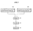
- Fig. 7 is an explanatory view showing a method of fabricating the double-sided display device according to the above-described embodiment.
- the fabrication method includes the steps of: fabricating the self-emitting element areas 10A and 10B on the substrates 11A and 11B, respectively, and forming the lead wiring sections 20A and 20B of the self-emitting element areas 10A and 10B in parts of the ends of the substrates 11A and 11B, respectively (lead wiring formation and element section formation step: S1A and S1B) ; bonding the substrates 11A and 11B to each other so that the lead wiring sections 20A and 20B are positioned on the same side (bonding step: S2); and forming the cutout portions 21A and 21B in the parts of the sides of the substrates 11A and 11B where the lead wiring sections 20A and 20B are not formed (cutting step: S3). Thereafter, an inspection step S4 is conducted as needed.
- the lead wiring sections 20A and 20B and the self-emitting element areas 10A and 10B are formed for the respective substrates 11A and 11B (S1A and S1B).
- the pair of substrates 11A and 11B are bonded to each other so that their faces carrying the self-emitting element areas 10A and 10B face each other (S2).
- the display planes 1a and 1b are formed on the respective bottom face sides of the substrates 11A and 11B so as to be oriented in different directions.
- the substrates 11A and 11B are bonded to each other so that the lead wiring sections 20A and 20B are positioned on the same side.
- the cutout portions 21A and 21B are formed in the sides of the substrates 11A and 11B where the lead wiring sections 20A and 20B are not formed, for example, through a technique such as laser cutting (if a plurality of panels are formed on the large substrates 11A and 11B, the cutting for obtaining individual panels can be performed at this cutting step) . Then, various necessary inspections are performed on an individual panel, thereby obtaining the double-sided display device 1 as a product.
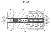
- Fig. 8 is an explanatory view (sectional view) showing an example of the present invention where organic EL elements are formed as the self-emitting element areas 10A and 10B (the same components as those in the above description are denoted by the same reference numerals, and the same description thereof is partially omitted) .
- the double-sided display device is obtained by bonding the substrates 11A and 11B through the bonding layer 12 to each other so that the self-emitting element areas 10A and 10B formed by organic EL elements are opposed to each other.
- the self-emitting element areas 10A and 10B are composed of a plurality of organic EL elements on the substrates 11A and 11B so as to interpose an organic material layer 33 including an organic light-emitting functional layer between a first electrode 31 and a second electrode 32.
- each of the organic EL elements has the following structure.
- a silicon coating layer 11a is formed on each of the substrates 11A and 11B.
- the first electrode 31 formed on the silicon coating layer 11a is used as an anode formed of a transparent electrode such as an ITO. Then, an insulating film 34 is formed on the first electrode 31 so that light-emitting areas 30R, 30G, and 30B are exposed through the insulating film 34. Then, in the light-emitting areas 30R, 30G, and 30B, a hole transport layer 33a, a light-emitting layer 33b, and an electron transport layer 33c are deposited on the first electrode 31. Then, the second electrode 32 made of a metal material such as Al is formed thereon so as to be used as a cathode.
- a transparent electrode such as an ITO.
- the organic EL elements are formed in the sealed space M formed by bonding the substrates 11A and 11B to each other through the bonding layer 12. In this manner, the organic EL elements are formed to have a bottom-emission structure in which light is obtained through the substrates 11A and 11B.
- an end 32a of the second electrode 32 is connected to a lead wiring 41.
- the lead wiring 41 is formed in a pattern while a second electrode layer 41c made of the same material and at the same fabrication step as those of the first electrode 31 is being insulated from the first electrode 31 by the insulating layer 34.
- a first electrode layer 41b forming a low resistance wiring portion containing a silver-palladium (AgPd) alloy or the like is formed.
- a protective coating film 41a made of IZO or the like is formed as needed.
- the lead wirings 41 are put together in the ends of the substrates 11A and 11B, respectively, thereby forming the lead wiring sections 20A and 20B.
- the driving system is not limited thereto.
- the self-emitting element areas 10A and 10B may be constituted to be driven by an active driving method.
- each of the substrates 11A and 11B It is preferred to use a flat plate-like or film-like substrate having transparency as each of the substrates 11A and 11B.
- the substrates 11A and 11B may be formed of glass, plastic or the like.
- the combination of the hole transport layer 33a, the light-emitting layer 33b, and the electron transport layer 33c is generally used as the organic material layer 33, as descried above.
- the hole transport layer 33a, the light-emitting layer 33b, and the electron transport layer 33c may be provided in plural in number instead of providing only one layer for each. Either one or both of the hole transport layer 33a and the electron transport layer 33b may be omitted.
- An organic material layer such as a hole injection layer, an electron injection layer, and a hole blocking layer may be added in accordance with an intended application.
- a conventionally used material (may be a polymeric material or a low-molecular material) can be appropriately selected for the hole transport layer 33a, the light-emitting layer 33b, and the electron transport layer 33c.
- Examples of the light-emitting material for forming the light-emitting layer 33b include any materials that emit light (produces fluorescence) when returning from a singlet excited state to a ground state and that emit light (produces phosphorescence) when returning from a triplet excited state through a singlet excited state to a ground state.
- a thermally curable adhesive, a chemically curable (two-part mixture) adhesive, a photo (ultraviolet)-curable adhesive or the like can be used as an adhesive for forming the bonding layer 12.
- a material include acrylic resins, epoxy resins, polyesters, polyolefins, and the like.
- an ultraviolet-curable epoxy resin adhesive having high quick curability, which does not need a heat treatment is preferred.
- the self-emitting element areas 10A and 10B may display a single color or a plurality of colors.
- an RGB selective deposition method can be used.
- a method using the combination of a monochromatic light-emitting functional layer such as white or blue and a color filter or a color changing layer made of a fluorescent material a CF method or a CCM method
- a method of radiating an electromagnetic wave on a light-emitting area of a monochromatic light-emitting functional layer or the like so as to achieve the light emission of a plurality of colors a photobleaching method
- a method of vertically depositing at least two unit display areas to form a single unit display area a SOLED (transparent Stacked OLED) method) and the like can be used.
- the double-sided display device includes: the pair of substrates 11A and 11B, on which the self-emitting element areas 10A and 10B are respectively formed, being bonded to each other so that their faces carrying the self-emitting element areas 10A and 10B face each other; and the display planes 1a and 1b formed on the bottom face sides of the respective substrates 11A and 11B so as to be oriented in opposite directions.
- the lead wiring sections 20A and 20B formed in the respective ends of the substrates 11A and 11B can be easily connected to a driving circuit component, a wiring substrate, or the like.
- the space where the panel of the double-sided display device 1 is placed or where the entire module including a driving circuit component, a wiring substrate, and the like is placed can be reduced.
- the double-sided display device having high effectiveness for mounting it on small electronic equipment can be obtained.
Landscapes
- Devices For Indicating Variable Information By Combining Individual Elements (AREA)
- Electroluminescent Light Sources (AREA)
Applications Claiming Priority (2)
| Application Number | Priority Date | Filing Date | Title |
|---|---|---|---|
| JP2004067169A JP4455904B2 (ja) | 2004-03-10 | 2004-03-10 | 両面表示装置及びその製造方法 |
| JP2004067169 | 2004-03-10 |
Publications (1)
| Publication Number | Publication Date |
|---|---|
| EP1575340A2 true EP1575340A2 (de) | 2005-09-14 |
Family
ID=34824571
Family Applications (1)
| Application Number | Title | Priority Date | Filing Date |
|---|---|---|---|
| EP05005049A Withdrawn EP1575340A2 (de) | 2004-03-10 | 2005-03-08 | Doppelseitige Anzeigevorrichtung und Verfahren zu ihrer Herstellung |
Country Status (4)
| Country | Link |
|---|---|
| US (1) | US7211938B2 (de) |
| EP (1) | EP1575340A2 (de) |
| JP (1) | JP4455904B2 (de) |
| CN (1) | CN1667670A (de) |
Families Citing this family (30)
| Publication number | Priority date | Publication date | Assignee | Title |
|---|---|---|---|---|
| WO2006022389A1 (ja) * | 2004-08-27 | 2006-03-02 | Pioneer Corporation | プローブ、並びに記録装置、再生装置及び記録再生装置 |
| US7656365B2 (en) * | 2005-03-28 | 2010-02-02 | Chad Byron Moore | Double-sided fiber-based displays |
| US20070120478A1 (en) * | 2005-11-28 | 2007-05-31 | Au Optronics Corporation | Double-sided display device and method of making same |
| JP5000128B2 (ja) * | 2005-11-30 | 2012-08-15 | 東北パイオニア株式会社 | 自発光パネル及びその製造方法 |
| US8038495B2 (en) | 2006-01-20 | 2011-10-18 | Samsung Mobile Display Co., Ltd. | Organic light-emitting display device and manufacturing method of the same |
| KR100673765B1 (ko) | 2006-01-20 | 2007-01-24 | 삼성에스디아이 주식회사 | 유기전계발광 표시장치 및 그 제조방법 |
| KR100635514B1 (ko) | 2006-01-23 | 2006-10-18 | 삼성에스디아이 주식회사 | 유기전계발광표시장치 및 그 제조방법 |
| JP4456092B2 (ja) | 2006-01-24 | 2010-04-28 | 三星モバイルディスプレイ株式會社 | 有機電界発光表示装置及びその製造方法 |
| JP4624309B2 (ja) * | 2006-01-24 | 2011-02-02 | 三星モバイルディスプレイ株式會社 | 有機電界発光表示装置及びその製造方法 |
| US8164257B2 (en) * | 2006-01-25 | 2012-04-24 | Samsung Mobile Display Co., Ltd. | Organic light emitting display and method of fabricating the same |
| KR100688796B1 (ko) * | 2006-01-25 | 2007-03-02 | 삼성에스디아이 주식회사 | 유기전계발광 표시 장치 및 그의 제작 방법 |
| KR100671641B1 (ko) * | 2006-01-25 | 2007-01-19 | 삼성에스디아이 주식회사 | 유기 전계 발광 표시장치 및 그 제조 방법 |
| KR100688795B1 (ko) | 2006-01-25 | 2007-03-02 | 삼성에스디아이 주식회사 | 유기전계발광 표시장치 및 그 제조방법 |
| KR100685853B1 (ko) | 2006-01-25 | 2007-02-22 | 삼성에스디아이 주식회사 | 유기전계발광표시장치 및 그 제조방법 |
| KR100732808B1 (ko) * | 2006-01-26 | 2007-06-27 | 삼성에스디아이 주식회사 | 유기전계발광 표시장치의 제조방법 |
| KR100671647B1 (ko) * | 2006-01-26 | 2007-01-19 | 삼성에스디아이 주식회사 | 유기전계발광 표시 장치 |
| JP4633674B2 (ja) | 2006-01-26 | 2011-02-16 | 三星モバイルディスプレイ株式會社 | 有機電界発光表示装置及びその製造方法 |
| KR100671639B1 (ko) * | 2006-01-27 | 2007-01-19 | 삼성에스디아이 주식회사 | 유기 전계 발광 표시장치 및 그 제조 방법 |
| KR100688790B1 (ko) * | 2006-01-27 | 2007-03-02 | 삼성에스디아이 주식회사 | 유기 전계 발광 표시장치 및 그 제조 방법 |
| KR100703446B1 (ko) * | 2006-02-21 | 2007-04-03 | 삼성에스디아이 주식회사 | 유기 전계 발광표시장치의 제조방법 |
| KR100703519B1 (ko) * | 2006-02-21 | 2007-04-03 | 삼성에스디아이 주식회사 | 유기 전계 발광표시장치의 제조방법 |
| KR100732817B1 (ko) | 2006-03-29 | 2007-06-27 | 삼성에스디아이 주식회사 | 유기전계발광 표시장치 및 그 제조방법 |
| US7923924B2 (en) * | 2007-04-03 | 2011-04-12 | Tsinghua University | Organic electroluminescent display/source with anode and cathode leads |
| US10180746B1 (en) | 2009-02-26 | 2019-01-15 | Amazon Technologies, Inc. | Hardware enabled interpolating sensor and display |
| US9740341B1 (en) * | 2009-02-26 | 2017-08-22 | Amazon Technologies, Inc. | Capacitive sensing with interpolating force-sensitive resistor array |
| US9785272B1 (en) | 2009-07-31 | 2017-10-10 | Amazon Technologies, Inc. | Touch distinction |
| US9244562B1 (en) | 2009-07-31 | 2016-01-26 | Amazon Technologies, Inc. | Gestures and touches on force-sensitive input devices |
| US8810524B1 (en) | 2009-11-20 | 2014-08-19 | Amazon Technologies, Inc. | Two-sided touch sensor |
| JP6106486B2 (ja) * | 2013-03-26 | 2017-03-29 | 株式会社カネカ | 有機elモジュール |
| JPWO2015079543A1 (ja) * | 2013-11-28 | 2017-03-16 | パイオニア株式会社 | 発光装置 |
Family Cites Families (2)
| Publication number | Priority date | Publication date | Assignee | Title |
|---|---|---|---|---|
| JPH08153586A (ja) | 1994-11-28 | 1996-06-11 | Nippondenso Co Ltd | 多色発光el装置 |
| JP2004014316A (ja) | 2002-06-07 | 2004-01-15 | Rohm Co Ltd | 両面表示有機エレクトロルミネセンスディスプレイモジュール及び情報端末 |
-
2004
- 2004-03-10 JP JP2004067169A patent/JP4455904B2/ja not_active Expired - Fee Related
-
2005
- 2005-03-08 EP EP05005049A patent/EP1575340A2/de not_active Withdrawn
- 2005-03-09 US US11/074,657 patent/US7211938B2/en not_active Expired - Fee Related
- 2005-03-09 CN CNA2005100536240A patent/CN1667670A/zh active Pending
Also Published As
| Publication number | Publication date |
|---|---|
| US7211938B2 (en) | 2007-05-01 |
| CN1667670A (zh) | 2005-09-14 |
| JP4455904B2 (ja) | 2010-04-21 |
| US20050200798A1 (en) | 2005-09-15 |
| JP2005257866A (ja) | 2005-09-22 |
Similar Documents
| Publication | Publication Date | Title |
|---|---|---|
| US7211938B2 (en) | Double-sided display device and method of fabricating the same | |
| JP6568180B2 (ja) | 有機発光表示装置 | |
| US6853411B2 (en) | Light-producing high aperture ratio display having aligned tiles | |
| KR101736930B1 (ko) | 플렉서블 유기발광 디스플레이 장치 | |
| EP1895593B1 (de) | Organische lichtemittierende Anzeige | |
| US20040080032A1 (en) | Semiconductor device and manufacturing method thereof, electro optic device, liquid crystal display device, electronics device | |
| KR20170059523A (ko) | 표시 장치, 타일형 표시 장치 및 이의 제조 방법 | |
| KR20200085835A (ko) | 터치 디스플레이 패널, 플렉서블 디스플레이 장치 및 터치 디스플레이 패널을 제조하는 방법 | |
| KR102660145B1 (ko) | 표시장치와 그의 제조방법 | |
| EP1575337A2 (de) | Doppelseitige Anzeigevorrichtung und Verfahren zu ihrer Herstellung | |
| US20060066236A1 (en) | Electronic apparatus, double-sided display panel and method of manufacturing the double-sided display panel | |
| TWI423718B (zh) | 有機電致發光裝置及具有此有機電致發光裝置的電子裝置 | |
| KR20240145450A (ko) | 유기발광 표시장치와 그의 제조방법 | |
| JP5114215B2 (ja) | 光デバイス、および光デバイスの製造方法 | |
| WO2005036935A1 (en) | Double-sided organic electroluminescent display | |
| CN114664886A (zh) | 电致发光显示装置 | |
| KR102756741B1 (ko) | 표시장치 | |
| CN217562201U (zh) | 拼接显示器组件及显示装置 | |
| CN118434195A (zh) | 显示设备 | |
| KR100631121B1 (ko) | 유기전계발광표시소자 및 그 제조방법 | |
| KR100739651B1 (ko) | 유기 전계 발광 표시장치 및 이의 제조 방법 | |
| KR20070065588A (ko) | 유기 발광 소자 | |
| US20250386653A1 (en) | Display device including display module | |
| KR100766933B1 (ko) | 평판 표시장치 | |
| US20070164660A1 (en) | Dual-emission organic electroluminescent device |
Legal Events
| Date | Code | Title | Description |
|---|---|---|---|
| PUAI | Public reference made under article 153(3) epc to a published international application that has entered the european phase |
Free format text: ORIGINAL CODE: 0009012 |
|
| AK | Designated contracting states |
Kind code of ref document: A2 Designated state(s): AT BE BG CH CY CZ DE DK EE ES FI FR GB GR HU IE IS IT LI LT LU MC NL PL PT RO SE SI SK TR |
|
| AX | Request for extension of the european patent |
Extension state: AL BA HR LV MK YU |
|
| STAA | Information on the status of an ep patent application or granted ep patent |
Free format text: STATUS: THE APPLICATION HAS BEEN WITHDRAWN |
|
| 18W | Application withdrawn |
Effective date: 20080610 |