EP1575337A2 - Doppelseitige Anzeigevorrichtung und Verfahren zu ihrer Herstellung - Google Patents
Doppelseitige Anzeigevorrichtung und Verfahren zu ihrer Herstellung Download PDFInfo
- Publication number
- EP1575337A2 EP1575337A2 EP05005048A EP05005048A EP1575337A2 EP 1575337 A2 EP1575337 A2 EP 1575337A2 EP 05005048 A EP05005048 A EP 05005048A EP 05005048 A EP05005048 A EP 05005048A EP 1575337 A2 EP1575337 A2 EP 1575337A2
- Authority
- EP
- European Patent Office
- Prior art keywords
- substrates
- self
- emitting element
- display device
- double
- Prior art date
- Legal status (The legal status is an assumption and is not a legal conclusion. Google has not performed a legal analysis and makes no representation as to the accuracy of the status listed.)
- Withdrawn
Links
Images


Classifications
-
- H—ELECTRICITY
- H05—ELECTRIC TECHNIQUES NOT OTHERWISE PROVIDED FOR
- H05B—ELECTRIC HEATING; ELECTRIC LIGHT SOURCES NOT OTHERWISE PROVIDED FOR; CIRCUIT ARRANGEMENTS FOR ELECTRIC LIGHT SOURCES, IN GENERAL
- H05B33/00—Electroluminescent light sources
- H05B33/02—Details
- H05B33/04—Sealing arrangements, e.g. against humidity
-
- H—ELECTRICITY
- H05—ELECTRIC TECHNIQUES NOT OTHERWISE PROVIDED FOR
- H05B—ELECTRIC HEATING; ELECTRIC LIGHT SOURCES NOT OTHERWISE PROVIDED FOR; CIRCUIT ARRANGEMENTS FOR ELECTRIC LIGHT SOURCES, IN GENERAL
- H05B33/00—Electroluminescent light sources
- H05B33/12—Light sources with substantially two-dimensional [2D] radiating surfaces
- H05B33/14—Light sources with substantially two-dimensional [2D] radiating surfaces characterised by the chemical or physical composition or the arrangement of the electroluminescent material, or by the simultaneous addition of the electroluminescent material in or onto the light source
-
- H—ELECTRICITY
- H10—SEMICONDUCTOR DEVICES; ELECTRIC SOLID-STATE DEVICES NOT OTHERWISE PROVIDED FOR
- H10K—ORGANIC ELECTRIC SOLID-STATE DEVICES
- H10K59/00—Integrated devices, or assemblies of multiple devices, comprising at least one organic light-emitting element covered by group H10K50/00
- H10K59/80—Constructional details
- H10K59/87—Passivation; Containers; Encapsulations
- H10K59/874—Passivation; Containers; Encapsulations including getter material or desiccant
-
- H—ELECTRICITY
- H10—SEMICONDUCTOR DEVICES; ELECTRIC SOLID-STATE DEVICES NOT OTHERWISE PROVIDED FOR
- H10K—ORGANIC ELECTRIC SOLID-STATE DEVICES
- H10K59/00—Integrated devices, or assemblies of multiple devices, comprising at least one organic light-emitting element covered by group H10K50/00
- H10K59/90—Assemblies of multiple devices comprising at least one organic light-emitting element
- H10K59/95—Assemblies of multiple devices comprising at least one organic light-emitting element wherein all light-emitting elements are organic, e.g. assembled OLED displays
-
- H—ELECTRICITY
- H10—SEMICONDUCTOR DEVICES; ELECTRIC SOLID-STATE DEVICES NOT OTHERWISE PROVIDED FOR
- H10K—ORGANIC ELECTRIC SOLID-STATE DEVICES
- H10K59/00—Integrated devices, or assemblies of multiple devices, comprising at least one organic light-emitting element covered by group H10K50/00
- H10K59/10—OLED displays
- H10K59/12—Active-matrix OLED [AMOLED] displays
- H10K59/128—Active-matrix OLED [AMOLED] displays comprising two independent displays, e.g. for emitting information from two major sides of the display
-
- H—ELECTRICITY
- H10—SEMICONDUCTOR DEVICES; ELECTRIC SOLID-STATE DEVICES NOT OTHERWISE PROVIDED FOR
- H10K—ORGANIC ELECTRIC SOLID-STATE DEVICES
- H10K59/00—Integrated devices, or assemblies of multiple devices, comprising at least one organic light-emitting element covered by group H10K50/00
- H10K59/10—OLED displays
- H10K59/17—Passive-matrix OLED displays
- H10K59/176—Passive-matrix OLED displays comprising two independent displays, e.g. for emitting information from two major sides of the display
Definitions
- the present invention relates to a double-sided display device and a method of fabricating the same.
- EL organic electroluminescence
- PDP plasma display panel
- FED field emission display
- a display section is formed by arranging self-emitting elements on a substrate. Therefore, the display devices have attracted attention as display devices which are advantageous over liquid crystal displays requiring a backlight in possibility of reduction of power consumption as well as of thickness.
- a double-sided display device enabling the display on both sides can be formed.
- a double-sided display device formed by an organic EL display device is disclosed.
- a sealing structure for blocking organic EL elements formed on a substrate from the outside air is required because the organic EL element has a property of deteriorating its display performance when it is exposed to the outside air containing moisture and the like.
- a pair of substrates each being a transparent substrate on which organic EL elements are formed, are bonded to each other so that their faces carrying the organic EL elements face each other.
- the organic EL elements are sealed between the pair of substrates.
- a display plane is formed on the bottom face side of each of the substrates so that the display planes of the respective substrates are oriented in the opposite directions, thereby achieving the display on both sides.
- the entire substrate is not necessarily used as a display plane. It often happens that the area of a display plane formed on one side of a double-sided display device differs from the area of a display plane formed on the other side, and that the position of a display plane formed on one side of a double-sided display device is not coincident with the position of a display plane formed on the other side, and the like. In such a case, according to the above-described conventional technique for sealing the organic EL elements between two substrates, a vacant space is formed on the substrate in the sealed space. Therefore, it is hardly considered that the double-sided display device effectively uses the space as a display panel unit required to occupy a smaller space.
- the present invention has an object of coping with the above-described problems. Specifically, in a double-sided display device including a pair of substrates each including a self-emitting element area formed thereon, the substrate being bonded to each other so that each of the self-emitting element areas is provided within a sealed space formed by the bonding, the present invention has objects of effectively using the sealed space, effectively excluding the outgas entering the sealed space upon or after bonding of the pair of substrates, and the like.
- a double-sided display device and a method of fabricating the same according to the present invention include at least a configuration according to each of the following independent aspects.
- a double-sided display device comprises: a pair of substrates; self-emitting element areas formed on the pair of substrates, respectively, the self-emitting element areas being provided in a sealed space formed by bonding the pair of substrates to each other; and display planes each being formed on each bottom face of the substrates so as to be oriented in opposite directions, wherein a desiccant is provided in a space on at least one of the substrates within the sealed space.
- a double-sided display device comprises: a pair of substrates; self-emitting element areas formed on the pair of substrates, respectively, the self-emitting element areas being provided in a sealed space formed by bonding the pair of substrates to each other; and display planes each being formed on each bottom face of the substrates so as to be oriented in opposite directions, wherein a driving circuit component is provided in a space on at least one of the substrates within the sealed space.
- a method of fabricating a double-sided display device comprises the steps of: providing any one of a desiccant and a driving circuit component in a space on a face of at least one of the substrates, on which the self-emitting element area is formed, after formation of the self-emitting element areas on the respective substrates; and arranging the one of the desiccant and the driving circuit component in the sealed space formed by bonding the pair of substrates to each other.
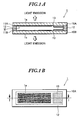
- FIGs. 1A and 1B are explanatory views showing a structure of a double-sided display device according to an embodiment of the present invention
- FIG. 1A is a sectional view taken along the line I-I in Fig. 1B
- Fig. 1B is a plan view
- a double-sided display device 1 has the following structure.
- Self-emitting element areas 11A and 11B are formed on a pair of substrates 10A and 10B, respectively.
- Each of the self-emitting element areas 11A and 11B is provided in a sealed space M formed by bonding the pair of substrates 10A and 10B to each other.
- display planes 1a and 1b are formed on the bottom face sides of the substrates 10A and 10B, respectively, so as to be oriented in the opposite directions.
- Each of the substrates 10A and 10B is formed of a transparent orsemi-transparentsubstrate.
- the self-emitting element are as 11A and 11B respectively formed on the substrates 10A and 10B have a bottom-emission structure for emitting light toward the bottom face side through the substrates 10A and 10B.
- the substrates 10A and 10B are bonded to each other through a bonding layer 12 so as to form a sealed space M between the substrates 10A and 10B. In the sealed space M , the self-emitting element areas 11A and 11B are provided.
- the self-emitting element areas 11A and 11B are formed not on the entire surfaces of the substrates 10A and 10B in the sealed space M , respectively. Therefore, there exist spaces in the sealed space M where the self-emitting element areas 11A and 11B are not formed.
- desiccants 13 herein, the desiccant encompasses all materials having the function of eliminating moisture or the like in the sealed space M ) are provided in the spaces.
- the display device is first formed by the pair of substrates 10A and 10B. Therefore, a solid display device can be formed. Moreover, since two self-emitting element areas 11A and 11B for realizing the display on both sides are formed in the single sealed space M , the space efficiency in a thickness direction is high. As a result, a thin display device can be formed.
- the desiccants 13 can be provided by using vacant spaces formed in the sealed space M on the substrates 10A and 10B. Therefore, the space efficiency in a plane direction is also high. Accordingly, in combination with the above-described high space efficiency in the thickness direction, the reduction in the size of the display device can be made possible. Moreover, since the sufficient desiccants 13 can be provided within the sealed space M , the desiccants 13 can surely eliminate the outgas entering from the adhesive layer 21 or the like into the sealed space M upon or after bonding of the substrates 10A and 10B.
- the double-sided display device 1 which can keep good display performance for a long period of time and also enables the reduction in size, can be provided.
- a variation of the arrangement or the shape of the display planes 1a and 1b can be appropriately determined in accordance with an intended application.
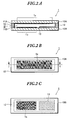
- Figs. 2A to 2C, 3A to 3C, and 4A to 4C are illustrative view showing examples (variations) where the arrangement or the shape of the display planes 1a and 1b is changed in the double-sided display device 1 according to the embodiment of the present invention
- Figs. 2A, 3A, and 4A are sectional views taken along the respective lines I-I in Figs. 2B, 3B, and 4B, respectively
- Figs. 2B, 3B, and 4B are plan views
- Figs. 2C, 3C, and 4C are rear views.
- the same sections as those in Fig. 1 are denoted by the same reference numerals, and part of description therefor will be omitted.
- the area of the self-emitting element area 11A formed on one substrate 10A differs from that of the self-emitting element area 11B formed on the other substrate 10B.
- the desiccant 13 is provided on the substrate 10B, on which the self-emitting element area 11B having the smaller area is formed.
- the double-sided display device 1 corresponds to the case where the display plane 1a on the substrate 10A side forms a larger main screen, whereas the display plane 1b on the substrate 10B side forms a smaller sub-screen.
- the desiccant 13 is provided using the vacant space.
- the position of the self-emitting element area 11A formed on one substrate 10A differs from that of the self-emitting element area 11B formed on the other substrate 10B.
- the self-emitting element area 11B on the other substrate 10B is provided so as to face the desiccant 13 provided at least on one substrate 10A.
- the self-emitting element area 11A is formed so as to form the annular display plane 1a on the side of the substrate 10A, whereas the self-emitting element area 11B is formed so that the display plane 1b is formed in the center on the side of the substrate 10B.
- the desiccant 13 is provided on the substrate 10B so as to face the self-emitting element area 11A, whereas another desiccant 13 is provided on the substrate 10A so as to face the self-emitting element area 11B.
- the effects produced by the desiccants 13 are directly applied on the self-emitting element areas 11A and 11B because the desiccants 13 are provided at the positions so as to face the self-emitting element areas 11A and 11B. Accordingly, the display performance of the self-emitting element areas 11A and 11B can be more surely maintained.
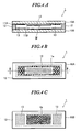
- Figs. 5 and 6 are illustrative views (sectional views) showing a double-sided display device according to another embodiment of the present invention.
- a concave engraved portion 10s is formed on the substrate 10A or 10B in the above-described embodiment so that the desiccant 13 is provided in the engraved portion 10s.
- the engraved portion 10s is formed on the substrate 10A or 10B by either one or both of etching and blasting.
- a thickness of the desiccant 13 is generally considerably large with respect to the thickness of each of the self-emitting element areas 11A and 11B. According to the above-described structure, however, the desiccant 13 is provided in the concave engraved portion 10s, so that the substrate 10A and 10B can be bonded to each other with a reduced distance therebetween. Accordingly, the thickness of the entire double-sided display device 1 can be further reduced.
- Fig. 7 is an explanatory view (sectional view) showing a double-sided display device according to a further embodiment of the present invention.
- the self-emitting element areas 11A and 11B are formed on the substrates 10A and 10B, respectively.
- the substrates 10A and 10B are bonded to each other to form the sealed space M therebetween.
- the self-emitting elements 11A and 11B are provided in the thus formed sealed space M .
- the display planes 1a and 1b are formed on the bottom face sides of the substrates 10A and 10B, respectively, so as to be oriented in the opposite directions.
- a driving circuit component 14 is provided in a space at least on one substrate 10B within the sealed space M .
- the area of the self-emitting element area 11A formed on the substrate 10A differs from that of the self-emitting element area 11B formed on the other substrate 10B.
- the driving circuit component 14 is provided on the substrate 10B, on which the self-emitting element area 11B having the smaller area is formed.
- the driving circuit component (a semiconductor chip or the like), which is generally provided external to the sealed space M , is provided using a vacant space in the sealed space M . Accordingly, the space efficiency in terms of plane can be improved to achieve the reduction in the size of the display device. Moreover, since the driving circuit component 14 is provided in the sealed space M , this structure also serves to protect the driving circuit component 14. Therefore, since it is no longer necessary to separately form a sealed space for the driving circuit component 14, the space efficiency in the thickness direction can be improved. Moreover, if the desiccant 13 is similarly provided in a vacant space, the above-described effects can also be obtained.
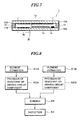
- Fig. 8 is an explanatory view showing a method of fabricating the double-sided display device according to the above-described embodiment.
- the self-emitting element areas 11A and 11B are formed on the substrates 10A and 10B, respectively (S1A and S1B).
- the desiccant 13 or the driving circuit component 14 is provided in the space on the surface of at least one substrate 10A (10B) on which the self-emitting element area 11A (11B) is formed (S2A and S2B).
- the substrates 10A and 10B are bonded to each other (S3).
- the substrates 10A and 10B are bonded to each other so that the self-emitting element areas 11A and 11B face each other in such a manner that the self-emitting element areas 11A and 11B, the desiccant 13, the driving circuit 14, and the like are provide in the sealed space M formed by bonding the substrates 10A and 10B to each other.
- the step of cutting the substrates into individual panels is added. After an inspection step (S4), which is conducted as needed, the double-sided display device 1 as a product is obtained.
- Fig. 9 is s an explanatory view (sectional view) showing an example of the present invention where organic EL elements are formed as the self-emitting element areas 11A and 11B (the same components as those in the above description are denoted by the same reference numerals, and the same description thereof is partially omitted).
- the double-sided display device is obtained by bonding the substrates 10A and 10B to each other through the bonding layer 12 so that the self-emitting element areas 11A and 11B formed by organic EL elements are opposed to each other.
- the self-emitting element areas 11A and 11B are composed of a plurality of organic EL elements formed on the substrates 10A and 10B so as to interpose an organic material layer 33 including an organic light-emitting functional layer between a first electrode 31 and a second electrode 32.
- each of the organic EL elements has the following structure.
- a silicon coating layer 10a is formed on each of the substrates 10A and 10B.
- the first electrode 31 formed on the silicon coating layer 10a is used as an anode formed of a transparent electrode such as an ITO. Then, an insulating film 34 is formed on the first electrode 31 so that light-emitting areas 30R, 30G, and 30B are exposed through the insulating film 34. Then, in the light-emitting areas 30R, 30G, and 30B, a hole transport layer 33a, a light-emitting layer 33b and an electron transport layer 33c are deposited on the first electrode 31. Then, the second electrode 32 made of a metal material such as Al is formed thereon so as to be used as a cathode.
- a transparent electrode such as an ITO.
- the organic EL elements are formed in the sealed space M formed by bonding the substrates 10A and 10B to each other through the bonding layer 12. In this manner, the organic EL elements are formed to have a bottom-emission structure, in which light is obtained through the substrates 10A and 10B.
- an end 32a of the second electrode 32 is connected to a lead wiring 41.
- the lead wiring 41 is formed in a pattern while a second electrode layer 41c made of the same material and at the same fabrication step as those of the first electrode 31 is being insulated from the first electrode 31 by the insulating layer 34.
- a first electrode layer 41b forming a low resistance wiring portion containing a silver-palladium (AgPd) alloy or the like is formed.
- a protective coating film 41a made of IZO or the like is formed as needed.
- the lead wirings 41 are put together in the ends of the substrates 10A and 10B, respectively, thereby forming the lead wiring sections 20A and 20B. Furthermore, the desiccants 13 are provided in the spaces on the substrates 10A and 10B within the sealed space M , respectively.
- the self-emitting element areas 11A and 11B supposing a passive driving method are shown in this case, the driving method is not limited thereto.
- the self-emitting element areas 11A and 11B may be constituted to be driven by an active driving method.
- each of the substrates 10A and 10B It is preferred to use a flat plate-like or film-like substrate having transparency as each of the substrates 10A and 10B.
- the substrates 10A and 10B may be formed of glass, plastic or the like.
- the combination of the hole transport layer 33a, the light-emitting layer 33b, and the electron transport layer 33c is generally used as the organic material layer 33, as descried above.
- the hole transport layer 33a, the light-emitting layer 33b, and the electron transport layer 33c may be provided in plural in number instead of providing only one layer for each. Either one or both of the hole transport layer 33a and the electron transport layer 33b may be omitted.
- An organic material layer such as a hole injection layer, an electron injection layer, and the like may be added in accordance with an intended application.
- a conventionally used material (may be a polymeric material or a low-molecular material) can be appropriately selected for the hole transport layer 33a, the light-emitting layer 33b, and the electron transport layer 33c.
- Examples of the light-emitting material for forming the light-emitting layer 33b include any materials that emit light (produces fluorescence) when returning from a singlet excited state to a ground state and that emit light (produces phosphorescence) when returning from a triplet excited state through a singlet excited state to a ground state.
- a thermally curable adhesive, a chemically curable (two-part mixture) adhesive, a photo (ultraviolet)-curable adhesive or the like can be used as an adhesive for forming the bonding layer 12.
- a material include acrylic resins, epoxy resins, polyesters, polyolefins, and the like.
- an ultraviolet-curable epoxy resin adhesive having high quick curability, which does not need a heat treatment is preferred.
- the desiccant 13 examples include a physical desiccant such as zeolite, a silica gel, carbon, and carbon nanotube, a chemical desiccant such as an alkali metal oxide, a metallic halide, and chlorine peroxide, a desiccant obtained by dissolving an organic metal complex in a petroleum solvent such as toluene, xylene, and an aliphatic organic solvent, and a desiccant obtained by dispersing desiccant particles in a binder such as polyethylene, polyisoprene, and polyvinyl cyanate, or the like.
- the desiccant 13 may be provided by adhering sheet-like desiccants onto the substrates 10A and 10B or by applying a resin containing a desiccating component onto the substrates 10A and 10B.
- the self-emitting element areas 11A and 11B may display a single color or a plurality of colors.
- an RGB selective deposition method can be used.
- a method using the combination of a monochromatic light-emitting functional layer such as white or blue and a color filter or a color changing layer made of a fluorescent material a CF method or a CCM method
- a method of radiating an electromagnetic wave on a light-emitting area of a monochromatic light-emitting functional layer or the like so as to achieve the light emission of a plurality of colors a photobleaching method
- a method of vertically depositing at least two unit display areas to form a single unit display area a SOLED (transparent Stacked OLED) method) and the like can be used.
- the double-sided display device includes, the pair of substrates 10A and 10B, on which the self-emitting element areas 11A and 11B are respectively formed, are bonded to each other so that their faces carrying the self-emitting elements 11A and 11B face each other.
- the display planes 1a and 1b are formed on the bottom face sides of the substrates 10A and 10B, respectively, so as to be oriented in the opposite directions. Since the sealed space M can be effectively used, the reduction in the size of the double-sided display device can be achieved. The outgas entering the sealed space M upon or after bonding of the substrates 10A and 10B can be effectively eliminated.
Landscapes
- Electroluminescent Light Sources (AREA)
- Devices For Indicating Variable Information By Combining Individual Elements (AREA)
Applications Claiming Priority (2)
| Application Number | Priority Date | Filing Date | Title |
|---|---|---|---|
| JP2004067170A JP2005259432A (ja) | 2004-03-10 | 2004-03-10 | 両面表示装置及びその製造方法 |
| JP2004067170 | 2004-03-10 |
Publications (1)
| Publication Number | Publication Date |
|---|---|
| EP1575337A2 true EP1575337A2 (de) | 2005-09-14 |
Family
ID=34824572
Family Applications (1)
| Application Number | Title | Priority Date | Filing Date |
|---|---|---|---|
| EP05005048A Withdrawn EP1575337A2 (de) | 2004-03-10 | 2005-03-08 | Doppelseitige Anzeigevorrichtung und Verfahren zu ihrer Herstellung |
Country Status (4)
| Country | Link |
|---|---|
| US (1) | US20050200268A1 (de) |
| EP (1) | EP1575337A2 (de) |
| JP (1) | JP2005259432A (de) |
| CN (1) | CN1668150A (de) |
Cited By (3)
| Publication number | Priority date | Publication date | Assignee | Title |
|---|---|---|---|---|
| EP1768154A2 (de) * | 2005-09-23 | 2007-03-28 | LG Electronics Inc. | Plasmaanzeigetafel und ihr Herstellungsverfahren |
| WO2007091215A1 (en) | 2006-02-10 | 2007-08-16 | Philips Intellectual Property & Standards Gmbh | A light emitting device |
| CN100474988C (zh) * | 2005-12-31 | 2009-04-01 | 友达光电股份有限公司 | 双面有机电致发光组件的封装结构及封装方法 |
Families Citing this family (12)
| Publication number | Priority date | Publication date | Assignee | Title |
|---|---|---|---|---|
| US20070120478A1 (en) * | 2005-11-28 | 2007-05-31 | Au Optronics Corporation | Double-sided display device and method of making same |
| KR100773937B1 (ko) | 2005-12-19 | 2007-11-07 | 주식회사 대우일렉트로닉스 | 오엘이디 디스플레이 패널 |
| CN100438066C (zh) * | 2005-12-22 | 2008-11-26 | 友达光电股份有限公司 | 双面显示装置 |
| KR100719596B1 (ko) * | 2005-12-30 | 2007-05-17 | 삼성에스디아이 주식회사 | 플라즈마 디스플레이 패널 |
| TWI308466B (en) * | 2006-05-02 | 2009-04-01 | Au Optronics Corp | Dual emission organic electroluminescent device |
| TWI336211B (en) | 2006-07-12 | 2011-01-11 | Au Optronics Corp | Double-sided display appratus |
| PL2082619T3 (pl) * | 2006-11-06 | 2023-03-13 | Agency For Science, Technology And Research | Nanocząstkowy enkapsulujący stos barierowy |
| CN104464549B (zh) * | 2010-10-14 | 2016-11-23 | 上海聚然智能科技有限公司 | 相邻电极等电势屏蔽显示屏 |
| CN104183579A (zh) * | 2013-05-21 | 2014-12-03 | 海洋王照明科技股份有限公司 | 一种有机电致发光器件及其制备方法 |
| CN104183588A (zh) * | 2013-05-21 | 2014-12-03 | 海洋王照明科技股份有限公司 | 一种有机电致发光器件及其制备方法 |
| CN104183587A (zh) * | 2013-05-21 | 2014-12-03 | 海洋王照明科技股份有限公司 | 一种有机电致发光器件及其制备方法 |
| TWI518897B (zh) * | 2013-07-02 | 2016-01-21 | 友達光電股份有限公司 | 具有自發光顯示面板的電子裝置 |
Family Cites Families (3)
| Publication number | Priority date | Publication date | Assignee | Title |
|---|---|---|---|---|
| KR100846581B1 (ko) * | 2002-09-19 | 2008-07-16 | 삼성에스디아이 주식회사 | 듀얼형 유기전자발광소자와 그 제조방법 |
| JP4050972B2 (ja) * | 2002-10-16 | 2008-02-20 | 株式会社 日立ディスプレイズ | 表示装置 |
| EP1614328A1 (de) * | 2003-04-08 | 2006-01-11 | Koninklijke Philips Electronics N.V. | Zweiseitige lichtemittierende vorrichtung |
-
2004
- 2004-03-10 JP JP2004067170A patent/JP2005259432A/ja active Pending
-
2005
- 2005-03-08 EP EP05005048A patent/EP1575337A2/de not_active Withdrawn
- 2005-03-09 CN CNA2005100536255A patent/CN1668150A/zh active Pending
- 2005-03-09 US US11/074,636 patent/US20050200268A1/en not_active Abandoned
Cited By (4)
| Publication number | Priority date | Publication date | Assignee | Title |
|---|---|---|---|---|
| EP1768154A2 (de) * | 2005-09-23 | 2007-03-28 | LG Electronics Inc. | Plasmaanzeigetafel und ihr Herstellungsverfahren |
| CN100474988C (zh) * | 2005-12-31 | 2009-04-01 | 友达光电股份有限公司 | 双面有机电致发光组件的封装结构及封装方法 |
| US8179029B2 (en) | 2006-02-07 | 2012-05-15 | Koninklijke Philips Electronics N.V. | Light emitting device including multiple OLEDs |
| WO2007091215A1 (en) | 2006-02-10 | 2007-08-16 | Philips Intellectual Property & Standards Gmbh | A light emitting device |
Also Published As
| Publication number | Publication date |
|---|---|
| US20050200268A1 (en) | 2005-09-15 |
| CN1668150A (zh) | 2005-09-14 |
| JP2005259432A (ja) | 2005-09-22 |
Similar Documents
| Publication | Publication Date | Title |
|---|---|---|
| US7211938B2 (en) | Double-sided display device and method of fabricating the same | |
| EP1575337A2 (de) | Doppelseitige Anzeigevorrichtung und Verfahren zu ihrer Herstellung | |
| US6965361B1 (en) | Method of manufacture of active matrix addressed polymer LED display | |
| EP1895593B1 (de) | Organische lichtemittierende Anzeige | |
| KR102448219B1 (ko) | 플렉시블 oled 디스플레이 모듈 | |
| US8917017B2 (en) | Organic el panel, panel-combined light emitting device, and method of manufacturing organic el panel | |
| TWI423718B (zh) | 有機電致發光裝置及具有此有機電致發光裝置的電子裝置 | |
| KR100934155B1 (ko) | 양면발광 유기전계 발광표시 장치 | |
| US20040245921A1 (en) | Full color display panel and color-separating substrate thereof | |
| JP5114215B2 (ja) | 光デバイス、および光デバイスの製造方法 | |
| US7122418B2 (en) | Method of fabricating organic light emitting diode device | |
| JP2006330185A (ja) | 電気光学パネル、封止部材及び電気光学パネルの製造方法 | |
| CN1976086B (zh) | 自发光面板及其制造方法 | |
| KR100631121B1 (ko) | 유기전계발광표시소자 및 그 제조방법 | |
| KR100623447B1 (ko) | 유기전계발광소자 | |
| KR100342192B1 (ko) | 유기 전계발광 디바이스 어셈블리 및 이의 제조 방법 | |
| KR100961954B1 (ko) | 유기발광디스플레이 제조방법 | |
| CN101944309A (zh) | 显示设备及其制造方法 | |
| KR100726994B1 (ko) | 유기 전계발광 표시장치 및 그 제조방법 | |
| KR100637499B1 (ko) | 유기 발광 표시장치 | |
| KR101010372B1 (ko) | 유기 전계 발광 소자 및 그 제조 방법 | |
| KR20150006646A (ko) | 유기 발광 표시 장치 | |
| KR20080087438A (ko) | 유기 발광 표시 장치 |
Legal Events
| Date | Code | Title | Description |
|---|---|---|---|
| PUAI | Public reference made under article 153(3) epc to a published international application that has entered the european phase |
Free format text: ORIGINAL CODE: 0009012 |
|
| AK | Designated contracting states |
Kind code of ref document: A2 Designated state(s): AT BE BG CH CY CZ DE DK EE ES FI FR GB GR HU IE IS IT LI LT LU MC NL PL PT RO SE SI SK TR |
|
| AX | Request for extension of the european patent |
Extension state: AL BA HR LV MK YU |
|
| STAA | Information on the status of an ep patent application or granted ep patent |
Free format text: STATUS: THE APPLICATION HAS BEEN WITHDRAWN |
|
| 18W | Application withdrawn |
Effective date: 20070907 |