EP1570422B1 - Schichtanordnung mit einer einen linsenartigen effekt erzeugenden beugungsoptisch wirksamen struktur - Google Patents
Schichtanordnung mit einer einen linsenartigen effekt erzeugenden beugungsoptisch wirksamen struktur Download PDFInfo
- Publication number
- EP1570422B1 EP1570422B1 EP03775318A EP03775318A EP1570422B1 EP 1570422 B1 EP1570422 B1 EP 1570422B1 EP 03775318 A EP03775318 A EP 03775318A EP 03775318 A EP03775318 A EP 03775318A EP 1570422 B1 EP1570422 B1 EP 1570422B1
- Authority
- EP
- European Patent Office
- Prior art keywords
- lens
- layer arrangement
- layer
- arrangement according
- grating
- Prior art date
- Legal status (The legal status is an assumption and is not a legal conclusion. Google has not performed a legal analysis and makes no representation as to the accuracy of the status listed.)
- Expired - Lifetime
Links
- 230000000694 effects Effects 0.000 title claims abstract description 32
- 230000003287 optical effect Effects 0.000 title claims description 10
- 239000000463 material Substances 0.000 claims description 8
- 238000010030 laminating Methods 0.000 claims description 6
- 239000002184 metal Substances 0.000 claims description 3
- 230000009467 reduction Effects 0.000 claims description 2
- 239000000049 pigment Substances 0.000 claims 1
- 229920003002 synthetic resin Polymers 0.000 abstract description 2
- 239000000057 synthetic resin Substances 0.000 abstract description 2
- 241000219739 Lens Species 0.000 description 83
- 239000010410 layer Substances 0.000 description 64
- 239000010408 film Substances 0.000 description 7
- 230000008901 benefit Effects 0.000 description 6
- 239000011888 foil Substances 0.000 description 6
- 238000000034 method Methods 0.000 description 6
- 230000005540 biological transmission Effects 0.000 description 5
- 239000004922 lacquer Substances 0.000 description 5
- 238000004519 manufacturing process Methods 0.000 description 5
- 239000000758 substrate Substances 0.000 description 4
- 240000004322 Lens culinaris Species 0.000 description 3
- 238000001465 metallisation Methods 0.000 description 3
- 239000004065 semiconductor Substances 0.000 description 3
- 230000000007 visual effect Effects 0.000 description 3
- 239000012790 adhesive layer Substances 0.000 description 2
- 239000003570 air Substances 0.000 description 2
- 230000008859 change Effects 0.000 description 2
- 239000003795 chemical substances by application Substances 0.000 description 2
- 239000011248 coating agent Substances 0.000 description 2
- 238000000576 coating method Methods 0.000 description 2
- 238000000609 electron-beam lithography Methods 0.000 description 2
- 238000004049 embossing Methods 0.000 description 2
- 229920002120 photoresistant polymer Polymers 0.000 description 2
- 230000008569 process Effects 0.000 description 2
- 239000010409 thin film Substances 0.000 description 2
- 239000012080 ambient air Substances 0.000 description 1
- 239000011247 coating layer Substances 0.000 description 1
- 239000003086 colorant Substances 0.000 description 1
- 230000003247 decreasing effect Effects 0.000 description 1
- 239000000203 mixture Substances 0.000 description 1
- 230000035699 permeability Effects 0.000 description 1
- 230000035945 sensitivity Effects 0.000 description 1
- 238000012795 verification Methods 0.000 description 1
Images
Classifications
-
- B—PERFORMING OPERATIONS; TRANSPORTING
- B42—BOOKBINDING; ALBUMS; FILES; SPECIAL PRINTED MATTER
- B42D—BOOKS; BOOK COVERS; LOOSE LEAVES; PRINTED MATTER CHARACTERISED BY IDENTIFICATION OR SECURITY FEATURES; PRINTED MATTER OF SPECIAL FORMAT OR STYLE NOT OTHERWISE PROVIDED FOR; DEVICES FOR USE THEREWITH AND NOT OTHERWISE PROVIDED FOR; MOVABLE-STRIP WRITING OR READING APPARATUS
- B42D25/00—Information-bearing cards or sheet-like structures characterised by identification or security features; Manufacture thereof
- B42D25/40—Manufacture
- B42D25/45—Associating two or more layers
- B42D25/465—Associating two or more layers using chemicals or adhesives
-
- G—PHYSICS
- G02—OPTICS
- G02B—OPTICAL ELEMENTS, SYSTEMS OR APPARATUS
- G02B5/00—Optical elements other than lenses
- G02B5/18—Diffraction gratings
-
- B—PERFORMING OPERATIONS; TRANSPORTING
- B42—BOOKBINDING; ALBUMS; FILES; SPECIAL PRINTED MATTER
- B42D—BOOKS; BOOK COVERS; LOOSE LEAVES; PRINTED MATTER CHARACTERISED BY IDENTIFICATION OR SECURITY FEATURES; PRINTED MATTER OF SPECIAL FORMAT OR STYLE NOT OTHERWISE PROVIDED FOR; DEVICES FOR USE THEREWITH AND NOT OTHERWISE PROVIDED FOR; MOVABLE-STRIP WRITING OR READING APPARATUS
- B42D25/00—Information-bearing cards or sheet-like structures characterised by identification or security features; Manufacture thereof
- B42D25/20—Information-bearing cards or sheet-like structures characterised by identification or security features; Manufacture thereof characterised by a particular use or purpose
- B42D25/29—Securities; Bank notes
-
- B—PERFORMING OPERATIONS; TRANSPORTING
- B42—BOOKBINDING; ALBUMS; FILES; SPECIAL PRINTED MATTER
- B42D—BOOKS; BOOK COVERS; LOOSE LEAVES; PRINTED MATTER CHARACTERISED BY IDENTIFICATION OR SECURITY FEATURES; PRINTED MATTER OF SPECIAL FORMAT OR STYLE NOT OTHERWISE PROVIDED FOR; DEVICES FOR USE THEREWITH AND NOT OTHERWISE PROVIDED FOR; MOVABLE-STRIP WRITING OR READING APPARATUS
- B42D25/00—Information-bearing cards or sheet-like structures characterised by identification or security features; Manufacture thereof
- B42D25/30—Identification or security features, e.g. for preventing forgery
- B42D25/305—Associated digital information
-
- B—PERFORMING OPERATIONS; TRANSPORTING
- B44—DECORATIVE ARTS
- B44C—PRODUCING DECORATIVE EFFECTS; MOSAICS; TARSIA WORK; PAPERHANGING
- B44C3/00—Processes, not specifically provided for elsewhere, for producing ornamental structures
- B44C3/02—Superimposing layers
-
- B—PERFORMING OPERATIONS; TRANSPORTING
- B44—DECORATIVE ARTS
- B44F—SPECIAL DESIGNS OR PICTURES
- B44F7/00—Designs imitating three-dimensional effects
-
- B—PERFORMING OPERATIONS; TRANSPORTING
- B42—BOOKBINDING; ALBUMS; FILES; SPECIAL PRINTED MATTER
- B42D—BOOKS; BOOK COVERS; LOOSE LEAVES; PRINTED MATTER CHARACTERISED BY IDENTIFICATION OR SECURITY FEATURES; PRINTED MATTER OF SPECIAL FORMAT OR STYLE NOT OTHERWISE PROVIDED FOR; DEVICES FOR USE THEREWITH AND NOT OTHERWISE PROVIDED FOR; MOVABLE-STRIP WRITING OR READING APPARATUS
- B42D25/00—Information-bearing cards or sheet-like structures characterised by identification or security features; Manufacture thereof
- B42D25/30—Identification or security features, e.g. for preventing forgery
- B42D25/324—Reliefs
Definitions
- the invention relates to a layer arrangement, in particular for transfer or laminating films, which has at least two successive layers of material , of which at least the in use the viewer facing (n) layer (s) is (are) transparent or semi-transparent and between which a Boundary surface is formed, which is provided at least in a surface area with a lens-like enlargement or reduction effect generating, diffraction-optically effective structure.
- transfer foils are understood as meaning in particular so-called embossing foils, which consist of a carrier film and a transfer layer which is removable from the latter and can be transferred to a substrate.
- the transfer layer of embossing foils is composed of different lacquer layers, which means that the term "material layer” used in the present invention is to be understood mainly in terms of a lacquer layer, but occasionally also in the sense of an adhesive layer.
- the invention also covers embodiments in which a "material layer” of the ambient air or a metallic, dielectric or semiconductor coating is formed.
- Laminating foils are substantially identical in their structure to transfer foils, but with the peculiarity that the synthetic resin or lacquer layers are not removable from the carrier film but can be fastened together with the carrier film on a substrate. Transfer or laminating films with a layer arrangement of the type mentioned are used in particular for security purposes, but also for decorative purposes.
- Layer arrangements of the type described in the introduction are already known and are used, for example, in the form of a uniformly appearing lens as a security element in certain recently launched credit cards (Amex-Blue).
- the surface area showing the lenticular effect has a relatively large diameter and essentially the shape of a circular lens.
- the structure of the known layer arrangement which produces the lenticular effect and has a diffraction-optical effect is a structure produced by means of a holographic technique and generally has sinusoidal surface profiles.
- Such holographically produced lenses have several shortcomings, apart from the fact that the holographic production of diffractive optical structures with lens effect with relatively little equipment is only possible when it comes to lenses with a circular or at best elliptical plan.
- holographic lenses for example, are that they do not appear to be very brilliant and generally have inhomogeneities, especially in the center region, which can significantly affect the visual appearance to be produced by the lens.
- Another shortcoming of holographically produced lenses is that it is practically impossible to achieve certain color effects with relatively great freedom of design.
- WO-A-97/19820 discloses a layer arrangement according to the preamble of claim 1.
- the invention is based on the object to propose a layer arrangement of the type mentioned, which does not have the mentioned shortcomings of the known, holographically generated lens structures with sinusoidal surface course, ie, to make the lenticular effect generating structures such that they are reasonable in apparatus and Time can be made very precise and in a variety of designs, that further the efficiency and luminosity of the lenticular structure effect compared to holographically generated structures is significantly improved and that finally at least one compared to holographically generated structures considerably expanded freedom in terms of color effects achieved.
- the invention proposes that the lens-like effect generating, diffraction-optically effective structure (hereinafter always “lens structure”) in such a way that they are in terms of their Grid frequency and optionally further lattice constants over the surface area continuously changing lattice structure, which is either a binary structure or designed such that the respective edges of the lattice grooves of the lattice structure parallel to each other and approximately parallel to a perpendicular to the main plane of the boundary layer, while - at least averaged over the entire flank-the angle of the respective other flanks of the grid grooves changes substantially continuously with respect to a perpendicular to the main plane of the boundary layer over the area, the grid depth (9) of the lens structures being at most 10 ⁇ m.
- a "binary structure” means a structure in which the groove grooves and grid lands each have a substantially rectangular cross-section, however, to produce the lensing effect, the lattice constant must change continuously from the center of the lens to the edge thereof In general, both the land and the groove width of the binary grid is changed. Binary gratings can be easily produced using appropriate masks with sufficient fineness, which results on the one hand in very high accuracy and on the other hand in comparatively low production costs.
- the other claimed embodiment of lattice structures is preferably produced by means of so-called "direct writing” by means of laser or electron beam lithography machines, in the use of which it is easily possible to produce very specific lattice structures and in particular the claimed structure, whereafter a flank of the corresponding lattice grooves each approximately perpendicular to the main plane of the lattice forming the lens, while the other flank is obliquely arranged with the lattice groove tapering towards the bottom of the furrow.
- lens structures according to the invention When lens structures according to the invention are used, on the one hand, there is the advantage of being able to produce a higher efficiency compared to holographically produced lens structures, with the result that the image formed with the aid of the lens or the corresponding decorative or security effect appears more brilliant , Furthermore, the lens structures according to the invention can be produced with very high accuracy-in comparison to holographically produced structures-whereby the visual appearance is markedly improved. Finally, it is possible by suitable choice of the lattice constants (grating frequency, grating depth, etc.) in the lens structures according to the invention to achieve special color effects or to control the color effects over the overall profile of the lens structure in a predetermined manner.
- the lattice constants grating frequency, grating depth, etc.
- Lens structures according to the invention thus have, in addition to the commonality of the small "thickness", a wide variety of advantages over holographically produced lens structures.
- Layer arrangements with a lens structure according to the invention can produce corresponding special optical effects both when viewed in transmission and in reflection.
- the layers adjacent to the interface are transparent and have a distinct, preferably at least 0.2 different refractive index. Due to the difference in the refractive index, it is achieved that the lens effect of the interface, despite the fact that the light passes through the layer arrangement, but causes a clearly visible effect.
- the lattice structure can not be covered on one side but connected to air.
- the interface is at least partially provided with a reflection-enhancing layer, wherein the reflection-enhancing layer is expediently a, for example vapor-deposited, metal layer.
- the reflection-enhancing layer is expediently a, for example vapor-deposited, metal layer.
- a transparent layer with a correspondingly high refractive index as a reflection-enhancing layer, in which case it would be possible to achieve a certain degree of permeability of the layer arrangement.
- Thin-film arrangements of the known combinations or semiconductor layers could also be used.
- the known credit card formed by a layer arrangement of the generic type holographically generated security element comprises only a circular lens structure.
- a diffractive lens structure according to the invention it is possible to arrange a plurality of lens structures distributed over the surface of the layer arrangement, which on the one hand yields much more interesting effects (in the case of use for decorative purposes) or, if the lens structure is part of a security element is, also allows to increase the safety effect. expedient In such a case, the plurality of lens structures are arranged in a grid, whereby the verification can be facilitated. But also an at least partially overlapping of the lens structures would be conceivable, wherein an interleaving would even be possible in the way that different lens structures appear depending on the viewing angle.
- lens structures or lens structure arrangements becomes particularly simple when, as provided according to the invention, the lens structures are formed essentially circular with concentrically extending grid lines.
- the lens structures have a diameter between 0.15 and 300 mm, preferably between 3 and 50 mm.
- the lattice depth of the lens structures is smaller than 5 .mu.m, preferably smaller than 3 .mu.m, such lattice structures can be introduced without problems into the lacquer layers conventionally provided in transfer or laminating foils, which have approximately this thickness ,
- the binary structure has approximately the same depth over the entire surface of the lens structure.
- the production is particularly simple.
- the transparent layer (s) adhered to the observer is (are) dyed pigment-free.
- the layer arrangement according to the invention comprises two material layers 1, 2 each, which form therebetween an interface 3, for example metallised, e.g. a vapor-deposited metal layer can be provided.
- one of the material layers 1, 2 may be formed by air.
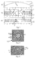
- the diameter of the lenses in Figure 1 is shown on the x-axis in arbitrary units, as it does not depend on the exact size or the exact diameter of the lens structures. However, the diameter of the lens structures is generally between 0.15 and 300 mm, preferably between 3 and 50 mm, the focal length of the lenses usually being between the value of the lens diameter and five times that value.
- the thickness or height of the corresponding layer 1, 2 or structure is plotted on the y-axis in FIG. 1, the values given being the phase difference in radians.
- a certain wavelength of light eg 550 nm for the maximum sensitivity of the human eye
- the thickness of the layer arrangement according to Figure 1a) must be at least ten times as large as the thickness of the layer arrangement according to Figure 1b) and even about twenty times as large as the thickness of the layer arrangement of Figure 1c). That the layer arrangements of FIGS.
- Layers 1 and 2 of the layer arrangement are generally coating layers of corresponding composition, wherein at least the lacquer layer facing the observer (in the present case, in general, the layer 1) must be substantially transparent, although it may be colored.
- the layers may be an adhesive layer or the layer facing the viewer may even be omitted.
- the layer 2 may also be transparent, but also translucent or opaque. If, on the other hand, the layer arrangement according to the invention is to be used in transmission, for example to cover a visible feature present on a substrate, the layer 2 must also be transparent. In this case, the interface 3 will not be provided with a generally opaque metallization. Instead, the refractive index of the two transparent layers 1 and 2 will be selected differently (the difference in the refractive index should preferably be at least 0.2) so that, despite the use of two transparent layers, the effect produced by the interface 3 becomes optically sufficiently clearly visible.
- the lens structure according to FIG. 1b is usually produced in a so-called "direct writing process", ie in a process in which the material is either removed by means of a laser in accordance with the desired profile or a photoresist is exposed according to the desired profile by means of a laser or an electron beam lithography device, and then the desired profile or its negative profile is obtained by developing the photoresist.
- This procedure offers the advantage that it is possible to produce very different lattice structures and, in particular, lattice cross sections, for example also so-called blaze lattices for certain applications, it being possible in particular to achieve that the angle ⁇ between the edges 4 of the lattice grooves running obliquely in FIG.
- the binary structure according to FIG. 1c) is produced using corresponding masks.
- the essential characteristic of the binary structure according to FIG. 1c) can be seen in that both the grating grooves 7 and the grating webs 8 are substantially rectangular in cross section.
- Another special feature of the structure according to Figure 1c) is to be seen in the fact that the grating depth is uniform over the entire lens structure 9, which offers the advantage in particular in the production that neither different exposure times of the material removing agent provided with different intensities of the mask through the corresponding Substrate acting agent must be worked.
- Figure 2 is schematically (actually the distances of the grid lines are much lower) shown a lens-like element, which is made with a lens structure according to Figure 1b), the plan view of Figure 2 clearly the ever decreasing distance between the grid bars or the can be constantly seen from the center of the circular lens to its edge increasing grid frequency.
- the inclination of the visible in the plan view of Figure 2 lattice edges 4 from the center of the lens to the outside is constantly changing and substantially continuously.
- the grid edges 5 perpendicular to the lens main plane are clearly visible in the form of dark lines in FIG.
- FIG. 3 shows a further possibility of how diffractive lens structures can be provided in a layer arrangement according to the invention.
- FIG. 3 which could be realized, for example, in the case of a decorative transfer or laminating film, circular lens structures are arranged distributed over the surface of the film in a plurality of surface areas arranged in a grid, which in principle can correspond to the lens structures of FIG.
- the arrangement is chosen so that not the outer grid grooves corresponding to Figure 2 are partially cut off. Rather, the lens structures 10 of FIG. 3 are each obtained in a circular manner.
- the interspaces in the form of spherical squares resulting from a sequence of corresponding lens-structure circles are filled by correspondingly shaped diffraction structures 11, which can likewise produce a lens effect, for example the lens structures 10 showing the effect of converging lenses, while FIG the structures 11 act as diverging lenses, whereby the optical effect of both lens types can be quasi strengthened.
- a demetallization may be provided in register with the lens structures.
- the lens structures do not have to be circular, as shown generally in the drawing.
- An advantage of using diffractive lens structures is precisely that they can also be superimposed on other shapes (so-called free-form surfaces) in order, for example, to generate three-dimensional structures.
Landscapes
- Business, Economics & Management (AREA)
- Accounting & Taxation (AREA)
- Finance (AREA)
- Physics & Mathematics (AREA)
- General Physics & Mathematics (AREA)
- Optics & Photonics (AREA)
- Health & Medical Sciences (AREA)
- Chemical & Material Sciences (AREA)
- Chemical Kinetics & Catalysis (AREA)
- General Chemical & Material Sciences (AREA)
- General Health & Medical Sciences (AREA)
- Toxicology (AREA)
- Engineering & Computer Science (AREA)
- Manufacturing & Machinery (AREA)
- Diffracting Gratings Or Hologram Optical Elements (AREA)
- Credit Cards Or The Like (AREA)
- Eyeglasses (AREA)
- Lenses (AREA)
Applications Claiming Priority (3)
| Application Number | Priority Date | Filing Date | Title |
|---|---|---|---|
| DE10254499 | 2002-11-22 | ||
| DE10254499A DE10254499B4 (de) | 2002-11-22 | 2002-11-22 | Schichtanordnung mit einer einen linsenartigen Effekt erzeugenden beugungsoptisch wirksamen Struktur |
| PCT/EP2003/012451 WO2004049250A1 (de) | 2002-11-22 | 2003-11-07 | Schichtanordnung mit einer einen linsenartigen effekt erzeugenden beugungsoptisch wirksamen struktur |
Publications (2)
| Publication Number | Publication Date |
|---|---|
| EP1570422A1 EP1570422A1 (de) | 2005-09-07 |
| EP1570422B1 true EP1570422B1 (de) | 2007-05-16 |
Family
ID=32318619
Family Applications (1)
| Application Number | Title | Priority Date | Filing Date |
|---|---|---|---|
| EP03775318A Expired - Lifetime EP1570422B1 (de) | 2002-11-22 | 2003-11-07 | Schichtanordnung mit einer einen linsenartigen effekt erzeugenden beugungsoptisch wirksamen struktur |
Country Status (14)
| Country | Link |
|---|---|
| US (1) | US7227690B2 (enExample) |
| EP (1) | EP1570422B1 (enExample) |
| JP (1) | JP4510636B2 (enExample) |
| KR (1) | KR100974682B1 (enExample) |
| CN (1) | CN100419789C (enExample) |
| AT (1) | ATE362627T1 (enExample) |
| AU (1) | AU2003283371B2 (enExample) |
| DE (2) | DE10254499B4 (enExample) |
| ES (1) | ES2287538T3 (enExample) |
| MY (1) | MY138939A (enExample) |
| PL (1) | PL375554A1 (enExample) |
| RU (1) | RU2317574C2 (enExample) |
| TW (1) | TWI306514B (enExample) |
| WO (1) | WO2004049250A1 (enExample) |
Cited By (1)
| Publication number | Priority date | Publication date | Assignee | Title |
|---|---|---|---|---|
| DE102010025775A1 (de) | 2010-07-01 | 2012-01-05 | Giesecke & Devrient Gmbh | Sicherheitselement sowie Wertdokument mit einem solchen Sicherheitselement |
Families Citing this family (22)
| Publication number | Priority date | Publication date | Assignee | Title |
|---|---|---|---|---|
| DE10254500B4 (de) * | 2002-11-22 | 2006-03-16 | Ovd Kinegram Ag | Optisch variables Element und dessen Verwendung |
| US7251398B2 (en) * | 2004-08-26 | 2007-07-31 | Interuniversitair Microelektronica Centrum (Imec) | Method for providing an optical interface and devices according to such methods |
| DE102004044459B4 (de) | 2004-09-15 | 2009-07-09 | Ovd Kinegram Ag | Sicherheitsdokument mit transparenten Fenstern |
| DE102005017169B4 (de) | 2005-04-13 | 2023-06-22 | Ovd Kinegram Ag | Transferfolie |
| DE102005017170B4 (de) | 2005-04-13 | 2010-07-01 | Ovd Kinegram Ag | Transferfolie, Verfahren zu deren Herstellung sowie Mehrschichtkörper und dessen Verwendung |
| DE102005027380B4 (de) † | 2005-06-14 | 2009-04-30 | Ovd Kinegram Ag | Sicherheitsdokument |
| DE102005061749A1 (de) | 2005-12-21 | 2007-07-05 | Giesecke & Devrient Gmbh | Optisch variables Sicherheitselement und Verfahren zu seiner Herstellung |
| US7973990B2 (en) * | 2006-04-27 | 2011-07-05 | Ricoh Company, Ltd. | Optical scanning device, optical writing device, and image forming apparatus |
| US8133638B2 (en) * | 2006-05-30 | 2012-03-13 | Brady Worldwide, Inc. | All-polymer grating microstructure |
| TW200913238A (en) * | 2007-06-04 | 2009-03-16 | Sony Corp | Optical member, solid state imaging apparatus, and manufacturing method |
| ES2320520B1 (es) * | 2007-11-21 | 2010-03-04 | Joaquin Devesa Company | Procedimiento de obtencion de una lamina lenticular y lamina asi obtenida. |
| DE102010019766A1 (de) | 2010-05-07 | 2011-11-10 | Giesecke & Devrient Gmbh | Verfahren zur Erzeugung einer Mikrostruktur auf einem Träger |
| FR2959830B1 (fr) | 2010-05-07 | 2013-05-17 | Hologram Ind | Composant optique d'authentification et procede de fabrication dudit composant |
| RU2430836C1 (ru) | 2010-07-29 | 2011-10-10 | Федеральное Государственное Унитарное Предприятие "Гознак" (Фгуп "Гознак") | Многослойный защитный элемент с переменным оптическим эффектом и защищенный от подделки документ |
| CN102981194B (zh) * | 2012-11-23 | 2015-04-01 | 中国科学院物理研究所 | 单片式光学元件以及单片式衍射光学元件的设计方法 |
| FR3000112B1 (fr) | 2012-12-20 | 2015-03-06 | Arjowiggins Security | Structure de securite. |
| DE102015100280A1 (de) | 2015-01-09 | 2016-07-14 | Ovd Kinegram Ag | Verfahren zur Herstellung von Sicherheitselementen sowie Sicherheitselemente |
| GB2545387A (en) * | 2015-07-24 | 2017-06-21 | De La Rue Int Ltd | Security device and method of manufacturing thereof |
| GB201513096D0 (en) | 2015-07-24 | 2015-09-09 | Rue De Int Ltd | Diffractive security device and method of manufacturing thereof |
| JP2018114696A (ja) | 2017-01-19 | 2018-07-26 | 凸版印刷株式会社 | 表示体 |
| WO2019063778A1 (en) * | 2017-09-29 | 2019-04-04 | Sicpa Holding Sa | OPTICAL SAFETY THIN MEMBER AND METHOD FOR DESIGNING SAME |
| DE102018103236A1 (de) | 2018-02-14 | 2019-08-14 | Leonhard Kurz Stiftung & Co. Kg | Sicherheitselement und Verfahren zur Herstellung eines Sicherheitselements |
Family Cites Families (21)
| Publication number | Priority date | Publication date | Assignee | Title |
|---|---|---|---|---|
| CA1267173A (en) | 1985-09-23 | 1990-03-27 | Thomas I. Bradshaw | Sheet containing contour-dependent directional image and method for forming the same |
| EP0219012B1 (de) * | 1985-10-15 | 1993-01-20 | GAO Gesellschaft für Automation und Organisation mbH | Datenträger mit einem optischen Echtheitsmerkmal sowie Verfahren zur Herstellung und Prüfung des Datenträgers |
| JPH06160610A (ja) * | 1989-12-26 | 1994-06-07 | Xerox Corp | 不連続多位相フレネルレンズ製造方法 |
| GB9309673D0 (en) * | 1993-05-11 | 1993-06-23 | De La Rue Holographics Ltd | Security device |
| CN1063552C (zh) * | 1995-02-28 | 2001-03-21 | 中国科学技术大学 | 一种量子线超微细图形的制作方法 |
| RU2103180C1 (ru) * | 1995-05-15 | 1998-01-27 | Инженерный информационно-коммерческий центр (предприятие "Инком Лтд") | Информационная карточка |
| JP3618465B2 (ja) * | 1996-05-31 | 2005-02-09 | オリンパス株式会社 | 回折光学素子、およびそれを用いる光学装置 |
| JP3618464B2 (ja) * | 1995-08-29 | 2005-02-09 | オリンパス株式会社 | 回折光学素子、およびそれを用いる光学装置 |
| DE69636991T2 (de) * | 1995-11-28 | 2007-12-06 | Ovd Kinegram Ag | Optischer Informationsträger |
| JPH10116016A (ja) * | 1996-10-09 | 1998-05-06 | Dainippon Printing Co Ltd | 光回折パターン形成体 |
| AUPO289296A0 (en) * | 1996-10-10 | 1996-10-31 | Securency Pty Ltd | Self-verifying security documents |
| US5969864A (en) * | 1997-09-25 | 1999-10-19 | Raytheon Company | Variable surface relief kinoform optical element |
| JP3479449B2 (ja) * | 1998-02-04 | 2003-12-15 | 沖電気工業株式会社 | 反射型回折光学素子の製造方法 |
| US6324004B1 (en) * | 1999-01-21 | 2001-11-27 | Ovd Kingegram Ag | Planar patterns with superimposed diffraction gratings |
| ES2236997T3 (es) * | 1999-08-12 | 2005-07-16 | Ovd Kinegram Ag | Soporte de datos. |
| EP1152369B1 (en) * | 1999-09-17 | 2007-03-21 | Dai Nippon Printing Co., Ltd. | Information recorded medium, device for reading the information, information recorded medium transfer foil, and method for producing information recorded medium |
| DE19949945A1 (de) * | 1999-10-16 | 2001-08-30 | Bundesdruckerei Gmbh | Datenträger mit Echtheitsmerkmalen und Herstellverfahren hierfür |
| JP2001332087A (ja) * | 2000-05-19 | 2001-11-30 | Nec Corp | センスアンプ回路 |
| JP3242638B2 (ja) * | 2000-07-07 | 2001-12-25 | キヤノン株式会社 | 表示素子および表示装置 |
| DE10054503B4 (de) * | 2000-11-03 | 2005-02-03 | Ovd Kinegram Ag | Lichtbeugende binäre Gitterstruktur und Sicherheitselement mit einer solchen Gitterstruktur |
| DE10123230A1 (de) * | 2001-05-12 | 2002-11-28 | Zeiss Carl | Diffraktives optisches Element sowie optische Anordnung mit einem diffraktiven optischen Element |
-
2002
- 2002-11-22 DE DE10254499A patent/DE10254499B4/de not_active Expired - Fee Related
-
2003
- 2003-11-07 JP JP2004554325A patent/JP4510636B2/ja not_active Expired - Lifetime
- 2003-11-07 WO PCT/EP2003/012451 patent/WO2004049250A1/de not_active Ceased
- 2003-11-07 AU AU2003283371A patent/AU2003283371B2/en not_active Ceased
- 2003-11-07 US US10/535,732 patent/US7227690B2/en not_active Expired - Lifetime
- 2003-11-07 EP EP03775318A patent/EP1570422B1/de not_active Expired - Lifetime
- 2003-11-07 AT AT03775318T patent/ATE362627T1/de active
- 2003-11-07 DE DE50307303T patent/DE50307303D1/de not_active Expired - Lifetime
- 2003-11-07 CN CNB2003801039085A patent/CN100419789C/zh not_active Expired - Fee Related
- 2003-11-07 RU RU2005119642/28A patent/RU2317574C2/ru active
- 2003-11-07 KR KR1020057009173A patent/KR100974682B1/ko not_active Expired - Fee Related
- 2003-11-07 PL PL03375554A patent/PL375554A1/xx not_active Application Discontinuation
- 2003-11-07 ES ES03775318T patent/ES2287538T3/es not_active Expired - Lifetime
- 2003-11-12 TW TW092131640A patent/TWI306514B/zh not_active IP Right Cessation
- 2003-11-18 MY MYPI20034412A patent/MY138939A/en unknown
Cited By (4)
| Publication number | Priority date | Publication date | Assignee | Title |
|---|---|---|---|---|
| DE102010025775A1 (de) | 2010-07-01 | 2012-01-05 | Giesecke & Devrient Gmbh | Sicherheitselement sowie Wertdokument mit einem solchen Sicherheitselement |
| WO2012000669A1 (de) | 2010-07-01 | 2012-01-05 | Giesecke & Devrient Gmbh | Sicherheitselement sowie wertdokument mit einem solchen sicherheitselement |
| US10870305B2 (en) | 2010-07-01 | 2020-12-22 | Giesecke+Devrient Currency Technology Gmbh | Security element as well as value document having such a security element |
| US12472763B2 (en) | 2010-07-01 | 2025-11-18 | Giesecke+Devrient Currency Technology Gmbh | Security element as well as value document having such a security element |
Also Published As
| Publication number | Publication date |
|---|---|
| ES2287538T3 (es) | 2007-12-16 |
| JP2006507526A (ja) | 2006-03-02 |
| CN100419789C (zh) | 2008-09-17 |
| CN1714370A (zh) | 2005-12-28 |
| DE10254499A1 (de) | 2004-06-17 |
| WO2004049250A1 (de) | 2004-06-10 |
| JP4510636B2 (ja) | 2010-07-28 |
| AU2003283371A1 (en) | 2004-06-18 |
| US20060072225A1 (en) | 2006-04-06 |
| ATE362627T1 (de) | 2007-06-15 |
| KR20050085086A (ko) | 2005-08-29 |
| DE50307303D1 (de) | 2007-06-28 |
| AU2003283371B2 (en) | 2008-04-03 |
| DE10254499B4 (de) | 2005-12-22 |
| MY138939A (en) | 2009-08-28 |
| RU2005119642A (ru) | 2006-01-27 |
| TWI306514B (en) | 2009-02-21 |
| PL375554A1 (en) | 2005-11-28 |
| TW200428019A (en) | 2004-12-16 |
| KR100974682B1 (ko) | 2010-08-06 |
| US7227690B2 (en) | 2007-06-05 |
| RU2317574C2 (ru) | 2008-02-20 |
| EP1570422A1 (de) | 2005-09-07 |
Similar Documents
| Publication | Publication Date | Title |
|---|---|---|
| EP1570422B1 (de) | Schichtanordnung mit einer einen linsenartigen effekt erzeugenden beugungsoptisch wirksamen struktur | |
| EP1562758B1 (de) | Optisch variables element und dessen verwendung | |
| EP2951031B1 (de) | Sicherheitselement mit rinnen- oder rippenförmigen strukturelementen | |
| EP2633344B1 (de) | Optisch variables flächenmuster | |
| EP2451650B2 (de) | Mehrschichtkörper | |
| EP2853411B1 (de) | Sicherheitselement mit Linsenrasterbild | |
| EP2934904B1 (de) | Sicherheitselement mit linsenrasterbild | |
| EP2727742B1 (de) | Sicherheitselement mit linsenrasterbild | |
| EP3581395A2 (de) | Mehrschichtkörper | |
| DE102010049600A1 (de) | Sicherheitselement mit optisch variablem Flächenmuster | |
| WO2009024265A1 (de) | Gitterbild | |
| EP3493996B1 (de) | Optisch variables sicherheitselement | |
| EP3253584B1 (de) | Optisch variables sicherheitselement | |
| WO2004077468A2 (de) | Sicherheitselement mit einer gitterstruktur | |
| EP3242801A1 (de) | Verfahren zur herstellung von sicherheitselementen sowie sicherheitselemente | |
| DE102017003281A1 (de) | Sicherheitselement mit Reliefstruktur und Herstellungsverfahren hierfür | |
| EP3600903A2 (de) | Sicherheitselement und verfahren zur herstellung eines sicherheitselements | |
| DE102022003386A1 (de) | Sicherheitselement mit Nanostrukturen | |
| DE102023121166A1 (de) | Optisch variables Durchsichtssicherheitselement, Datenträger und Herstellungsverfahren | |
| EP4353486A2 (de) | Sicherheitselement mit lichtbrechenden strukturen und farbwechsel |
Legal Events
| Date | Code | Title | Description |
|---|---|---|---|
| PUAI | Public reference made under article 153(3) epc to a published international application that has entered the european phase |
Free format text: ORIGINAL CODE: 0009012 |
|
| 17P | Request for examination filed |
Effective date: 20050507 |
|
| AK | Designated contracting states |
Kind code of ref document: A1 Designated state(s): AT BE BG CH CY CZ DE DK EE ES FI FR GB GR HU IE IT LI LU MC NL PT RO SE SI SK TR |
|
| AX | Request for extension of the european patent |
Extension state: AL LT LV MK |
|
| DAX | Request for extension of the european patent (deleted) | ||
| GRAP | Despatch of communication of intention to grant a patent |
Free format text: ORIGINAL CODE: EPIDOSNIGR1 |
|
| GRAS | Grant fee paid |
Free format text: ORIGINAL CODE: EPIDOSNIGR3 |
|
| GRAA | (expected) grant |
Free format text: ORIGINAL CODE: 0009210 |
|
| AK | Designated contracting states |
Kind code of ref document: B1 Designated state(s): AT BE BG CH CY CZ DE DK EE ES FI FR GB GR HU IE IT LI LU MC NL PT RO SE SI SK TR |
|
| PG25 | Lapsed in a contracting state [announced via postgrant information from national office to epo] |
Ref country code: FI Free format text: LAPSE BECAUSE OF FAILURE TO SUBMIT A TRANSLATION OF THE DESCRIPTION OR TO PAY THE FEE WITHIN THE PRESCRIBED TIME-LIMIT Effective date: 20070516 |
|
| REG | Reference to a national code |
Ref country code: GB Ref legal event code: FG4D Free format text: NOT ENGLISH |
|
| REG | Reference to a national code |
Ref country code: CH Ref legal event code: EP |
|
| REG | Reference to a national code |
Ref country code: IE Ref legal event code: FG4D Free format text: LANGUAGE OF EP DOCUMENT: GERMAN |
|
| REF | Corresponds to: |
Ref document number: 50307303 Country of ref document: DE Date of ref document: 20070628 Kind code of ref document: P |
|
| REG | Reference to a national code |
Ref country code: CH Ref legal event code: NV Representative=s name: FIAMMENGHI-FIAMMENGHI |
|
| GBT | Gb: translation of ep patent filed (gb section 77(6)(a)/1977) |
Effective date: 20070726 |
|
| REG | Reference to a national code |
Ref country code: SE Ref legal event code: TRGR |
|
| ET | Fr: translation filed | ||
| REG | Reference to a national code |
Ref country code: ES Ref legal event code: FG2A Ref document number: 2287538 Country of ref document: ES Kind code of ref document: T3 |
|
| REG | Reference to a national code |
Ref country code: IE Ref legal event code: FD4D |
|
| PG25 | Lapsed in a contracting state [announced via postgrant information from national office to epo] |
Ref country code: IE Free format text: LAPSE BECAUSE OF FAILURE TO SUBMIT A TRANSLATION OF THE DESCRIPTION OR TO PAY THE FEE WITHIN THE PRESCRIBED TIME-LIMIT Effective date: 20070516 Ref country code: DK Free format text: LAPSE BECAUSE OF FAILURE TO SUBMIT A TRANSLATION OF THE DESCRIPTION OR TO PAY THE FEE WITHIN THE PRESCRIBED TIME-LIMIT Effective date: 20070516 Ref country code: BG Free format text: LAPSE BECAUSE OF FAILURE TO SUBMIT A TRANSLATION OF THE DESCRIPTION OR TO PAY THE FEE WITHIN THE PRESCRIBED TIME-LIMIT Effective date: 20070816 Ref country code: PT Free format text: LAPSE BECAUSE OF FAILURE TO SUBMIT A TRANSLATION OF THE DESCRIPTION OR TO PAY THE FEE WITHIN THE PRESCRIBED TIME-LIMIT Effective date: 20071016 Ref country code: SI Free format text: LAPSE BECAUSE OF FAILURE TO SUBMIT A TRANSLATION OF THE DESCRIPTION OR TO PAY THE FEE WITHIN THE PRESCRIBED TIME-LIMIT Effective date: 20070516 |
|
| PG25 | Lapsed in a contracting state [announced via postgrant information from national office to epo] |
Ref country code: SK Free format text: LAPSE BECAUSE OF FAILURE TO SUBMIT A TRANSLATION OF THE DESCRIPTION OR TO PAY THE FEE WITHIN THE PRESCRIBED TIME-LIMIT Effective date: 20070516 |
|
| PLBE | No opposition filed within time limit |
Free format text: ORIGINAL CODE: 0009261 |
|
| STAA | Information on the status of an ep patent application or granted ep patent |
Free format text: STATUS: NO OPPOSITION FILED WITHIN TIME LIMIT |
|
| 26N | No opposition filed |
Effective date: 20080219 |
|
| PG25 | Lapsed in a contracting state [announced via postgrant information from national office to epo] |
Ref country code: GR Free format text: LAPSE BECAUSE OF FAILURE TO SUBMIT A TRANSLATION OF THE DESCRIPTION OR TO PAY THE FEE WITHIN THE PRESCRIBED TIME-LIMIT Effective date: 20070817 |
|
| PG25 | Lapsed in a contracting state [announced via postgrant information from national office to epo] |
Ref country code: RO Free format text: LAPSE BECAUSE OF FAILURE TO SUBMIT A TRANSLATION OF THE DESCRIPTION OR TO PAY THE FEE WITHIN THE PRESCRIBED TIME-LIMIT Effective date: 20070516 |
|
| PG25 | Lapsed in a contracting state [announced via postgrant information from national office to epo] |
Ref country code: MC Free format text: LAPSE BECAUSE OF NON-PAYMENT OF DUE FEES Effective date: 20071130 |
|
| PG25 | Lapsed in a contracting state [announced via postgrant information from national office to epo] |
Ref country code: EE Free format text: LAPSE BECAUSE OF FAILURE TO SUBMIT A TRANSLATION OF THE DESCRIPTION OR TO PAY THE FEE WITHIN THE PRESCRIBED TIME-LIMIT Effective date: 20070516 |
|
| PG25 | Lapsed in a contracting state [announced via postgrant information from national office to epo] |
Ref country code: CY Free format text: LAPSE BECAUSE OF FAILURE TO SUBMIT A TRANSLATION OF THE DESCRIPTION OR TO PAY THE FEE WITHIN THE PRESCRIBED TIME-LIMIT Effective date: 20070516 |
|
| PG25 | Lapsed in a contracting state [announced via postgrant information from national office to epo] |
Ref country code: LU Free format text: LAPSE BECAUSE OF NON-PAYMENT OF DUE FEES Effective date: 20071107 |
|
| PG25 | Lapsed in a contracting state [announced via postgrant information from national office to epo] |
Ref country code: HU Free format text: LAPSE BECAUSE OF FAILURE TO SUBMIT A TRANSLATION OF THE DESCRIPTION OR TO PAY THE FEE WITHIN THE PRESCRIBED TIME-LIMIT Effective date: 20071117 Ref country code: TR Free format text: LAPSE BECAUSE OF FAILURE TO SUBMIT A TRANSLATION OF THE DESCRIPTION OR TO PAY THE FEE WITHIN THE PRESCRIBED TIME-LIMIT Effective date: 20070516 |
|
| REG | Reference to a national code |
Ref country code: FR Ref legal event code: PLFP Year of fee payment: 13 |
|
| REG | Reference to a national code |
Ref country code: FR Ref legal event code: PLFP Year of fee payment: 14 |
|
| REG | Reference to a national code |
Ref country code: FR Ref legal event code: PLFP Year of fee payment: 15 |
|
| PGFP | Annual fee paid to national office [announced via postgrant information from national office to epo] |
Ref country code: SE Payment date: 20191125 Year of fee payment: 17 |
|
| PGFP | Annual fee paid to national office [announced via postgrant information from national office to epo] |
Ref country code: BE Payment date: 20191121 Year of fee payment: 17 |
|
| PGFP | Annual fee paid to national office [announced via postgrant information from national office to epo] |
Ref country code: AT Payment date: 20191119 Year of fee payment: 17 |
|
| REG | Reference to a national code |
Ref country code: SE Ref legal event code: EUG |
|
| REG | Reference to a national code |
Ref country code: AT Ref legal event code: MM01 Ref document number: 362627 Country of ref document: AT Kind code of ref document: T Effective date: 20201107 |
|
| REG | Reference to a national code |
Ref country code: BE Ref legal event code: MM Effective date: 20201130 |
|
| PG25 | Lapsed in a contracting state [announced via postgrant information from national office to epo] |
Ref country code: SE Free format text: LAPSE BECAUSE OF NON-PAYMENT OF DUE FEES Effective date: 20201108 Ref country code: AT Free format text: LAPSE BECAUSE OF NON-PAYMENT OF DUE FEES Effective date: 20201107 |
|
| PGFP | Annual fee paid to national office [announced via postgrant information from national office to epo] |
Ref country code: ES Payment date: 20211216 Year of fee payment: 19 |
|
| PGFP | Annual fee paid to national office [announced via postgrant information from national office to epo] |
Ref country code: IT Payment date: 20211130 Year of fee payment: 19 Ref country code: CH Payment date: 20211123 Year of fee payment: 19 |
|
| PG25 | Lapsed in a contracting state [announced via postgrant information from national office to epo] |
Ref country code: BE Free format text: LAPSE BECAUSE OF NON-PAYMENT OF DUE FEES Effective date: 20201130 |
|
| PGFP | Annual fee paid to national office [announced via postgrant information from national office to epo] |
Ref country code: NL Payment date: 20221118 Year of fee payment: 20 Ref country code: GB Payment date: 20221123 Year of fee payment: 20 Ref country code: FR Payment date: 20221118 Year of fee payment: 20 Ref country code: DE Payment date: 20220609 Year of fee payment: 20 Ref country code: CZ Payment date: 20221026 Year of fee payment: 20 |
|
| REG | Reference to a national code |
Ref country code: CH Ref legal event code: PL |
|
| PG25 | Lapsed in a contracting state [announced via postgrant information from national office to epo] |
Ref country code: LI Free format text: LAPSE BECAUSE OF NON-PAYMENT OF DUE FEES Effective date: 20221130 Ref country code: CH Free format text: LAPSE BECAUSE OF NON-PAYMENT OF DUE FEES Effective date: 20221130 |
|
| PG25 | Lapsed in a contracting state [announced via postgrant information from national office to epo] |
Ref country code: IT Free format text: LAPSE BECAUSE OF NON-PAYMENT OF DUE FEES Effective date: 20221107 |
|
| REG | Reference to a national code |
Ref country code: DE Ref legal event code: R071 Ref document number: 50307303 Country of ref document: DE |
|
| REG | Reference to a national code |
Ref country code: NL Ref legal event code: MK Effective date: 20231106 |
|
| REG | Reference to a national code |
Ref country code: GB Ref legal event code: PE20 Expiry date: 20231106 |
|
| REG | Reference to a national code |
Ref country code: ES Ref legal event code: FD2A Effective date: 20231227 |
|
| PG25 | Lapsed in a contracting state [announced via postgrant information from national office to epo] |
Ref country code: GB Free format text: LAPSE BECAUSE OF EXPIRATION OF PROTECTION Effective date: 20231106 |
|
| PG25 | Lapsed in a contracting state [announced via postgrant information from national office to epo] |
Ref country code: ES Free format text: LAPSE BECAUSE OF NON-PAYMENT OF DUE FEES Effective date: 20221108 |
|
| PG25 | Lapsed in a contracting state [announced via postgrant information from national office to epo] |
Ref country code: GB Free format text: LAPSE BECAUSE OF EXPIRATION OF PROTECTION Effective date: 20231106 Ref country code: ES Free format text: LAPSE BECAUSE OF NON-PAYMENT OF DUE FEES Effective date: 20221108 Ref country code: CZ Free format text: LAPSE BECAUSE OF EXPIRATION OF PROTECTION Effective date: 20231107 |