EP1569266A2 - Procédé pour la fabrication d'une couche de siliciure, structure intermédiaire multicouche et structure multicouche - Google Patents
Procédé pour la fabrication d'une couche de siliciure, structure intermédiaire multicouche et structure multicouche Download PDFInfo
- Publication number
- EP1569266A2 EP1569266A2 EP04020632A EP04020632A EP1569266A2 EP 1569266 A2 EP1569266 A2 EP 1569266A2 EP 04020632 A EP04020632 A EP 04020632A EP 04020632 A EP04020632 A EP 04020632A EP 1569266 A2 EP1569266 A2 EP 1569266A2
- Authority
- EP
- European Patent Office
- Prior art keywords
- silicide film
- film
- silicon substrate
- multilayered
- nickel
- Prior art date
- Legal status (The legal status is an assumption and is not a legal conclusion. Google has not performed a legal analysis and makes no representation as to the accuracy of the status listed.)
- Withdrawn
Links
Images




Classifications
-
- H—ELECTRICITY
- H10—SEMICONDUCTOR DEVICES; ELECTRIC SOLID-STATE DEVICES NOT OTHERWISE PROVIDED FOR
- H10D—INORGANIC ELECTRIC SEMICONDUCTOR DEVICES
- H10D64/00—Electrodes of devices having potential barriers
- H10D64/01—Manufacture or treatment
- H10D64/011—Manufacture or treatment of electrodes ohmically coupled to a semiconductor
- H10D64/0111—Manufacture or treatment of electrodes ohmically coupled to a semiconductor to Group IV semiconductors
- H10D64/0112—Manufacture or treatment of electrodes ohmically coupled to a semiconductor to Group IV semiconductors using conductive layers comprising silicides
Definitions
- This invention relates to a method for fabricating a silicide film, and a multilayered intermediate structure for fabricating the same silicide film, and a multilayered structure containing the same silicide film.
- a metal film is deposited on a semiconductor substrate to form a multilayered structure, which is thermally treated to form a metal-semiconductor compound film as the metal/semiconductor junction electrode.
- titanium (Ti), cobalt (Co) or nickel (Ni) is employed as a metallic material to form a metallic silicon compound (silicide) film such as a titanium disilicide (TiSi 2 ) film, a cobalt disilicide (CoSi 2 ) film, a nickel monosilicide (NiSi) film or a nickel disilicide (NiSi 2 ) film.
- a metallic silicon compound (silicide) film such as a titanium disilicide (TiSi 2 ) film, a cobalt disilicide (CoSi 2 ) film, a nickel monosilicide (NiSi) film or a nickel disilicide (NiSi 2 ) film.
- the silicide film such as the CoSi 2 film and the NiSi 2 film can match in lattice constant to the silicon substrate by several %, the silicide film can be epitaxially grown on the silicon substrate to be a single crystalline film.
- the NiSi 2 film can match in lattice constant to the silicon substrate by 0.4%, the NiSi 2 film can be easily epitaxially grown on the silicon substrate by means of thermal treatment at 800°C or over. Therefore, the NiSi 2 is an ideal electrode material in the silicon-based element.
- the deposited nickel silicide film prior to the thermal treatment contains relatively much polycrystalline NiSi. Since the polycrystalline NiSi is thermally unstable, the polycrystalline NiSi agglomerates to form polycrystalline NiSi particles through the thermal treatment. As a result, the structure and the composition uniformity of the intended NiSi 2 epitaxial film may be deteriorated.
- NiSi 2 is an ideal electrode material for the silicon-based element, the inherent performance of the NiSi 2 can not be exhibited due to the above-mentioned problems, so that currently, the NiSi 2 can not be employed as the electrode material for the silicon-based element.
- this invention relates to a method for fabricating a silicide film, comprising the steps of:
- a silicon substrate is prepared, and a compound element-containing layer containing compound elements to compose an intended silicide film to be formed later is formed on the silicon substrate to form a multilayered intermediate structure.
- a titanium layer is formed between the silicon substrate and the compound element-containing layer. In this case, the boundary reaction between the silicon substrate and the compound element-containing layer can be prevented through thermal treatment by the titanium intermediate layer.
- the boundary surface between the silicon substrate and the silicide film can be formed flat in the order of atomic level.
- the intended silicide film can be formed at extremely low temperature, e.g., around 350°C. Therefore, the degradation of a silicide film with agglomeration is prevented due to the direct formation of the intended silicide film at low temperature without the prior formation of a thermally unstable polycrystalline NiSi film..
- the intended silicide film particularly a NiSi 2 film is maintained at a higher temperature, e.g., of 600°C or over after the formation, agglomerated particles can not be created. Therefore, the intended silicide film can exhibit uniform structure and composition at the higher temperature. As a result, the intended silicide film, particularly, the NiSi 2 film can be preferably employed as a practical electrode material of a silicon-based element also due to the high crystallinity of the epitaxial growth.
- the thermal treatment is carried out at 800°C or over.
- the thermal treatment is carried out only at 350°C or below. Therefore, the NiSi 2 film can be easily formed.
- the thickness of the titanium intermediate layer is set to 50nm or below. In this case, the above-mentioned function/effect of the titanium intermediate layer can be enhanced. Also, the remnant amount of titanium in the intended silicide film can be decreased, so that the performance deterioration of the intended silicide film due to the remnant titanium can be prevented.
- an additional thermal treatment can be carried out for the silicide film.
- the boundary surface between the silicon substrate and the silicide film can be flattened more precisely.
- the additional thermal treatment can be carried out, e.g., at 400°C or over.
- the fabricating method of the present invention can be applied for the fabrication of a silicide film such as a TiSi 2 film, a CoSi 2 film, or a NiSi 2 film, but preferably for the fabrication of the NiSi 2 film.
- a silicide film which has uniform structure and composition and whereby the boundary surface against a silicon substrate can be flattened for the use of a practical electrode material of a silicon-based element.
- Figs. 1 and 2 illustrate respective fabricating steps in the fabricating method of the present invention.
- a silicon substrate 11 is prepared, and a titanium intermediate layer 12 is formed on the silicon substrate 11.
- a compound element-containing layer containing compound elements to compose an intended silicide film to be formed later is formed on the titanium intermediate layer 12 to form a multilayered intermediate structure 10.
- a thermal treatment is carried out for the multilayered intermediate structure under vacuum atmosphere, nitrogen atmosphere or argon atmosphere to interdiffuse silicon elements of the silicon substrate 11 and the compound elements of the compound element-containing layer one another and thus, to form an intended silicide film 23 on the silicon substrate 11, as illustrated in Fig. 2.
- the titanium intermediate layer 12 is formed in order to prevent the boundary reaction between the silicon substrate 11 and the silicide film 23 through the thermal treatment for the fabrication of the silicide film 23. Therefore, no facet is created at the boundary surface 24 between the silicon substrate 11 and the silicide film 23, so that the boundary surface 24 can be flattened more precisely, e.g., in the order of atomic level. As a result, no concave-convex boundary surface is formed.
- the thermal treatment is carried out at relatively low temperature, e.g., of 350°C or below. Therefore, the intended silicide film 23 can be formed at the relatively low temperature. Therefore, the degradation of a silicide film with agglomeration is prevented due to the direct formation of the intended silicide film at low temperature without the prior formation of a thermally unstable polycrystalline NiSi film.
- the intended silicide film particularly a NiSi 2 film is maintained at a higher temperature, e.g., of 600°C or over after the formation, agglomerated particles can not be created. Therefore, the intended silicide film can exhibit uniform structure and composition at the higher temperature. As a result, the intended silicide film, particularly, the NiSi 2 film can be preferably employed as a practical electrode material of a silicon-based element also due to the high crystallinity of the epitaxial growth.
- the thickness of the titanium intermediate layer is desired to set the thickness of the titanium intermediate layer to 50nm or below, preferably 20nm or below, more preferably 5nm or below. In this case, the above-mentioned function/effect of the titanium intermediate layer can be more enhanced.
- the lower limit of the thickness of the titanium intermediate layer 12 is preferably set to 0.5nm in view of the same function/effect of the titanium intermediate layer.
- the titanium intermediate layer 12 is dispersed into the silicide film 23 through the thermal treatment, so that the silicide film 23 contains a small amount of Ti, in addition to the silicon elements and the compound elements.
- the thickness of the compound element-containing layer 13 may be appropriately controlled on the thickness of the intended silicide film 23. All of the compound element-containing layer 13 may be converted into the silicide film 23, but only a part of the compound element-containing layer 23 may be converted into the silicide film 23. If the thickness of the titanium intermediate layer 12 is set to 50nm or below, the thickness of the compound element-containing layer 13 may be set within 10-100nm. In this embodiment, as illustrated in Fig. 2, all of the compound element-containing layer 13 is converted into the silicide film 23.
- the silicide film can be formed as an epitaxial film by controlling the thermal treatment condition such as thermal treatment temperature. Therefore, the silicide film such as the CoSi 2 film, the NiSi film or the PtSi film can be used as a practical electrode material of a silicon based element.
- an additional thermal treatment can be carried out for the silicide film 23 after the formation as mentioned above.
- the boundary surface between the silicon substrate 11 and the silicide film 23 can be easily and effectively flattened more precisely.
- the boundary surface 24 can be formed flat in the order of atomic level under high reproducibility.
- the multilayered structure 20 made of the silicon substrate 11 and the NiSi 2 film 23 is heated at 400°C or over, particularly 600°C or over under a vacuum, nitrogen or argon atmosphere.
- the upper limit temperature of the additional thermal treatment may be set to 1000°C. If the additional thermal treatment is carried out beyond 1000°C, the boundary surface can not be more flattened. On the contrary, the boundary surface may be roughed, and the flatness of the boundary surface may be deteriorated.
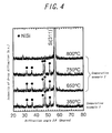
- a (100) Si substrate was prepared, and a titanium intermediate layer was formed in a thickness of 2nm on the Si substrate. Then, a nickel layer was formed in a thickness of 9nm on the titanium intermediate layer to form a multilayered intermediate structure.
- the multilayered intermediate structure was disposed in a vacuum condition, and thermally treated at 350°C for 30 minutes to form a nickel silicide film on the Si substrate.
- the multilayered intermediate structure was formed in the same manner as in Example 1. Then, the multilayered intermediate structure was disposed in a nitrogen atmosphere, and in addition, thermally treated within 550-850°C.
- the multilayered intermediate structure with no titanium intermediate layer was formed in the same manner as in Comparative Example 1, and in addition, thermally treated under the same condition as in Example 1.
- Fig. 3 are graphs illustrating the X-ray diffraction patterns of the nickel silicide films formed in Examples 1 and 2.
- Fig. 4 are graphs illustrating the X-ray diffraction patterns of the nickel silicide films formed in Comparative Examples 1 and 2.
- the temperature of 350°C means a thermal treatment temperature at the formation of the nickel silicide film
- the temperatures of 650°C, 750°C and 850°C mean additional thermal treatment temperatures, respectively.
- the nickel silicide film formed through the 850°C additional thermal treatment exhibits only peaks originated from C54-TiSi 2 crystal.
- the nickel silicide films obtained through the thermal treatment of 350°C and the additional thermal treatments of 650-850°C in Examples are epitaxial NiSi 2 films, respectively.
- a NiSi polycrystal is created through the 350°C thermal treatment. Then, the NiSi crystal phase exists after the additional thermal treatment within 650-750°C, but disappears after the additional thermal treatment at 850°C. In view of the matching of the X-ray diffraction peak of the NiSi 2 crystal phase to the one of the Si(311) crystal plane, it is turned out that at the additional thermal treatment at 850°C, a NiSi 2 phase is created in the nickel silicide film.
- Fig. 5 is a surface SEM photograph of the nickel silicide film obtained in Example 2
- Fig. 6 is a surface SEM photograph of the nickel silicide film obtained in Comparative Example 2.
- the nickel silicide films are formed through the additional thermal treatment of 750°C.
- the surface of the nickel silicide film in Example 2 according to the present invention is extremely uniform, but the surface of the nickel silicide film in Comparative Example 2 is not uniform. Also, on the analysis utilizing characteristic X-ray, it is turned out that the black areas in Fig. 6 mean exposed portions of the silicon substrate.
- Fig. 7 is a cross sectional TEM photograph of the nickel silicide film obtained in Example 2
- Fig. 8 is a cross sectional TEM photograph of the nickel silicide film obtained in Comparative Example 2.
- the nickel silicide films are formed through the additional thermal treatment of 850°C.
- the nickel silicide film in Example 2 according to the present invention can have a flat boundary surface in the order of atomic level. In the nickel silicide film in Comparative Example 2, however, ⁇ 111 ⁇ facets are locally created at the boundary surface, so that no flat boundary surface can be formed and the concave-convex boundary can be formed.
Landscapes
- Electrodes Of Semiconductors (AREA)
Applications Claiming Priority (2)
| Application Number | Priority Date | Filing Date | Title |
|---|---|---|---|
| JP2004051790A JP3879003B2 (ja) | 2004-02-26 | 2004-02-26 | シリサイド膜の作製方法 |
| JP2004051790 | 2004-02-26 |
Publications (1)
| Publication Number | Publication Date |
|---|---|
| EP1569266A2 true EP1569266A2 (fr) | 2005-08-31 |
Family
ID=34747513
Family Applications (1)
| Application Number | Title | Priority Date | Filing Date |
|---|---|---|---|
| EP04020632A Withdrawn EP1569266A2 (fr) | 2004-02-26 | 2004-08-31 | Procédé pour la fabrication d'une couche de siliciure, structure intermédiaire multicouche et structure multicouche |
Country Status (3)
| Country | Link |
|---|---|
| US (1) | US20050189652A1 (fr) |
| EP (1) | EP1569266A2 (fr) |
| JP (1) | JP3879003B2 (fr) |
Cited By (1)
| Publication number | Priority date | Publication date | Assignee | Title |
|---|---|---|---|---|
| CN104752182A (zh) * | 2013-12-30 | 2015-07-01 | 中国科学院上海微系统与信息技术研究所 | 一种利用Ti插入层制作NiSiGe材料的方法 |
Families Citing this family (4)
| Publication number | Priority date | Publication date | Assignee | Title |
|---|---|---|---|---|
| JP2007173743A (ja) * | 2005-12-26 | 2007-07-05 | Toshiba Corp | 半導体装置の製造方法 |
| JP5116003B2 (ja) * | 2006-02-27 | 2013-01-09 | セイコーエプソン株式会社 | シリサイドの形成方法及び半導体装置の製造方法 |
| JP2007242894A (ja) * | 2006-03-08 | 2007-09-20 | Toshiba Corp | 半導体装置およびその製造方法 |
| JP4920310B2 (ja) * | 2006-05-30 | 2012-04-18 | 株式会社東芝 | 半導体装置およびその製造方法 |
Family Cites Families (14)
| Publication number | Priority date | Publication date | Assignee | Title |
|---|---|---|---|---|
| US5047111A (en) * | 1985-03-16 | 1991-09-10 | Director-General Of The Agency Of Industrial Science And Technology | Method of forming a metal silicide film |
| JP2692554B2 (ja) * | 1993-12-16 | 1997-12-17 | 日本電気株式会社 | 半導体装置の製造方法 |
| US5861340A (en) * | 1996-02-15 | 1999-01-19 | Intel Corporation | Method of forming a polycide film |
| US6071782A (en) * | 1998-02-13 | 2000-06-06 | Sharp Laboratories Of America, Inc. | Partial silicidation method to form shallow source/drain junctions |
| US6492694B2 (en) * | 1998-02-27 | 2002-12-10 | Micron Technology, Inc. | Highly conductive composite polysilicon gate for CMOS integrated circuits |
| US6229167B1 (en) * | 1998-03-24 | 2001-05-08 | Rohm Co., Ltd. | Semiconductor device and method of manufacturing the same |
| US6440851B1 (en) * | 1999-10-12 | 2002-08-27 | International Business Machines Corporation | Method and structure for controlling the interface roughness of cobalt disilicide |
| US6730587B1 (en) * | 2000-12-07 | 2004-05-04 | Advanced Micro Devices, Inc. | Titanium barrier for nickel silicidation of a gate electrode |
| US6534871B2 (en) * | 2001-05-14 | 2003-03-18 | Sharp Laboratories Of America, Inc. | Device including an epitaxial nickel silicide on (100) Si or stable nickel silicide on amorphous Si and a method of fabricating the same |
| US6495460B1 (en) * | 2001-07-11 | 2002-12-17 | Advanced Micro Devices, Inc. | Dual layer silicide formation using a titanium barrier to reduce surface roughness at silicide/junction interface |
| US6958814B2 (en) * | 2002-03-01 | 2005-10-25 | Applied Materials, Inc. | Apparatus and method for measuring a property of a layer in a multilayered structure |
| US6873051B1 (en) * | 2002-05-31 | 2005-03-29 | Advanced Micro Devices, Inc. | Nickel silicide with reduced interface roughness |
| DE10245607B4 (de) * | 2002-09-30 | 2009-07-16 | Advanced Micro Devices, Inc., Sunnyvale | Verfahren zum Bilden von Schaltungselementen mit Nickelsilizidgebieten, die durch ein Barrierendiffusionsmaterial thermisch stabilisiert sind sowie Verfahren zur Herstellung einer Nickelmonosilizidschicht |
| US6787864B2 (en) * | 2002-09-30 | 2004-09-07 | Advanced Micro Devices, Inc. | Mosfets incorporating nickel germanosilicided gate and methods for their formation |
-
2004
- 2004-02-26 JP JP2004051790A patent/JP3879003B2/ja not_active Expired - Lifetime
- 2004-08-26 US US10/925,976 patent/US20050189652A1/en not_active Abandoned
- 2004-08-31 EP EP04020632A patent/EP1569266A2/fr not_active Withdrawn
Cited By (1)
| Publication number | Priority date | Publication date | Assignee | Title |
|---|---|---|---|---|
| CN104752182A (zh) * | 2013-12-30 | 2015-07-01 | 中国科学院上海微系统与信息技术研究所 | 一种利用Ti插入层制作NiSiGe材料的方法 |
Also Published As
| Publication number | Publication date |
|---|---|
| JP3879003B2 (ja) | 2007-02-07 |
| JP2005243923A (ja) | 2005-09-08 |
| US20050189652A1 (en) | 2005-09-01 |
Similar Documents
| Publication | Publication Date | Title |
|---|---|---|
| Mangelinck et al. | Enhancement of thermal stability of NiSi films on (100) Si and (111) Si by Pt addition | |
| KR0155587B1 (ko) | 반도체 웨이퍼의 실리콘 층 위에 규화 티탄 층을 형성하는 방법 | |
| US6720258B2 (en) | Method of fabricating a nickel silicide on a substrate | |
| US5567652A (en) | Method for manufacturing semiconductor device comprising cobalt silicide film | |
| US20120171864A1 (en) | Method of manufacturing semiconductor device | |
| Cabral Jr et al. | Low temperature formation of C54–TiSi 2 using titanium alloys | |
| NL8303341A (nl) | Werkwijze voor het produceren van een heterostructuur, welke een heteroepitaxiaal, uit meerdere bestanddelen opgebouwd materiaal omvat; voorwerp dat een heterostructuur omvat. | |
| CN100369219C (zh) | 使用Ni合金阻滞一硅化镍的结块作用 | |
| KR100763898B1 (ko) | 반도체 소자 제조방법 및 이에 의하여 제조된 반도체 소자 | |
| CN116387140A (zh) | 在碳化硅衬底之上制造金属硅化物层的方法和包括金属硅化物层的半导体器件 | |
| EP1569266A2 (fr) | Procédé pour la fabrication d'une couche de siliciure, structure intermédiaire multicouche et structure multicouche | |
| US20150024586A1 (en) | Method for producing a monocrystalline metal/semiconductor compound | |
| US6627919B2 (en) | Thermally stable nickel germanosilicide formed on SiGe | |
| Jones et al. | AlN as an encapsulate for annealing SiC | |
| JP3262676B2 (ja) | 半導体装置 | |
| Mangelinck et al. | Formation and stability of Ni (Pt) silicide on (100) Si and (111) Si | |
| US20240055256A1 (en) | Method for manufacturing a contact on a silicon carbide semiconductor substrate, and silicon carbide semiconductor device | |
| WO2001026143A1 (fr) | Procédé de fabrication d'un dispositif à semi-conducteur | |
| JP2002293697A (ja) | GaNエピタキシャル層の成長方法 | |
| Shiraki et al. | High quality NiSi2/Si epitaxial films grown by MBE | |
| JP3076243B2 (ja) | 半導体装置および該半導体装置の製造方法 | |
| Tai et al. | Effect of preamorphization implantation on C54–TiSi 2 formation in salicided narrow lines | |
| JP3700004B2 (ja) | コバルトシリサイド膜の作製方法、コバルトシリサイド膜、及びコバルトシリサイド膜作製用の多層膜中間構造体 | |
| Shi et al. | Growth of CoSi2 films on Si (100) substrates by a two-step method | |
| Tung | Growth of Epitaxial CoSi2 Through a Thin Interlayer |
Legal Events
| Date | Code | Title | Description |
|---|---|---|---|
| PUAI | Public reference made under article 153(3) epc to a published international application that has entered the european phase |
Free format text: ORIGINAL CODE: 0009012 |
|
| 17P | Request for examination filed |
Effective date: 20040831 |
|
| AK | Designated contracting states |
Kind code of ref document: A2 Designated state(s): AT BE BG CH CY CZ DE DK EE ES FI FR GB GR HU IE IT LI LU MC NL PL PT RO SE SI SK TR |
|
| AX | Request for extension of the european patent |
Extension state: AL HR LT LV MK |
|
| STAA | Information on the status of an ep patent application or granted ep patent |
Free format text: STATUS: THE APPLICATION IS DEEMED TO BE WITHDRAWN |
|
| 18D | Application deemed to be withdrawn |
Effective date: 20070301 |