EP1566890A1 - Analogfehlerbestimmung unter Verwendung von Abtastung in parallelen Zweigen - Google Patents
Analogfehlerbestimmung unter Verwendung von Abtastung in parallelen Zweigen Download PDFInfo
- Publication number
- EP1566890A1 EP1566890A1 EP05250673A EP05250673A EP1566890A1 EP 1566890 A1 EP1566890 A1 EP 1566890A1 EP 05250673 A EP05250673 A EP 05250673A EP 05250673 A EP05250673 A EP 05250673A EP 1566890 A1 EP1566890 A1 EP 1566890A1
- Authority
- EP
- European Patent Office
- Prior art keywords
- signal
- sampling switch
- analog
- sampling
- sampled signal
- Prior art date
- Legal status (The legal status is an assumption and is not a legal conclusion. Google has not performed a legal analysis and makes no representation as to the accuracy of the status listed.)
- Ceased
Links
Images

Classifications
-
- H—ELECTRICITY
- H03—ELECTRONIC CIRCUITRY
- H03M—CODING; DECODING; CODE CONVERSION IN GENERAL
- H03M1/00—Analogue/digital conversion; Digital/analogue conversion
- H03M1/06—Continuously compensating for, or preventing, undesired influence of physical parameters
-
- H—ELECTRICITY
- H03—ELECTRONIC CIRCUITRY
- H03M—CODING; DECODING; CODE CONVERSION IN GENERAL
- H03M1/00—Analogue/digital conversion; Digital/analogue conversion
- H03M1/06—Continuously compensating for, or preventing, undesired influence of physical parameters
- H03M1/08—Continuously compensating for, or preventing, undesired influence of physical parameters of noise
- H03M1/0836—Continuously compensating for, or preventing, undesired influence of physical parameters of noise of phase error, e.g. jitter
-
- H—ELECTRICITY
- H03—ELECTRONIC CIRCUITRY
- H03M—CODING; DECODING; CODE CONVERSION IN GENERAL
- H03M1/00—Analogue/digital conversion; Digital/analogue conversion
- H03M1/10—Calibration or testing
Definitions
- This invention relates in general to sampling methods for determining signal error, and more particularly to a method and system for determining analog error using parallel paths.
- a method for determining analog error of a signal includes receiving an input signal and sampling the input signal to generate a first sampled signal. The method also includes communicating the first sampled signal using a first communication path and a second communication path and sampling the first sampled signal from the first communication path to generate a second sampled signal. The method further includes converting the first sampled signal from the second communication path into a digital signal, storing the digital signal using a digital memory, comparing the second sampled signal to the digital signal, and determining an analog error of the input signal based on the comparison.
- Particular embodiments of the present invention may provide various technical advantages.
- One technical advantage of particular embodiments is reducing the number of high frequency components required to perform sampling and analysis.
- Particular embodiments of the present invention allow certain components to function at a relatively lower frequency compared to the frequency of the input signal. This allows circuits to be constructed with fewer high frequency components. The reduction in the number of high frequency components reduces the overall costs of the circuit as well as simplifying circuit design.
- Another technical advantage of particular embodiments is reduced difficulty associated with latency.
- the latency introduced into the circuit by the operation of components may cause the feedback to lag slightly behind the input signal. This may result in errors and/or inefficient function in the circuit.
- particular embodiments of the invented circuit may reduce the need for high-speed feedback, which may reduce the difficulties associated with latency.
- Still another technical advantage of particular embodiments of the present invention is reduction of state dependency.
- Particular embodiments of the present invention may be adapted to use equalization after sampling. This allows sampling switches to clear their states after each sampling iteration. Because it may take a significant amount of time compared to the period of the signal to switch a particular value of a sampling switch from, for example, high to low, not initializing the switch after every iteration may introduce inappropriate time delays, known as "jitter.”
- jitter By allowing equalization after switch iterations, particular embodiments of the present invention reduce problems associated with jitter. These and other aspects may help to enable applications that involve high-speed analog error analysis.
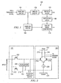
- FIGURE 1 illustrates a circuit 100 used to perform analysis of analog error.
- circuit 100 includes a sampling switch 101, an analog buffer 102, a decision slicer block 104, a switch-and-latch combination 106, a second sample switch 108, and an analog error comparison module 110.
- circuit 100 samples an input signal and calculates the degree of analog error.
- Analog error refers generally to the amount of deviation in amplitude between an incoming signal and the nominal high value of a corresponding digital system. The analog error is useful for determining the performance of a system and identifying areas of the system that may be degrading performance, such as components consuming an excessive amount of power.
- Sampling switches 101 and 108 represent any suitable components for receiving a high frequency signal, taking the value at predetermined time intervals in the signal, and outputting that value.
- Sampling switches 101 and 108 are capable of sampling signals in the gigahertz range.
- Sampling switches 101 and 108 may include any suitable electronic components, including components such as transistors, resistors, and constant current sources.
- Sampling switches 101 and 108 may advantageously include several high-speed components to allow sampling of high-frequency signals.
- Analog buffer 102 represents any suitable components for storing an incoming analog signal. Analog buffer 102 may include any suitable combination of electronic components or other forms of signal storage. In the depicted embodiment, analog buffer 102 buffers the output signal of first sample switch 101.
- Decision slicer block 104 represents any suitable components for converting the output of analog buffer 102 into a digital signal.
- Decision slicer 104 may include any combination of electronic or other components for analog to digital conversion.
- decision slicer 104 includes several metal oxide semiconductor effect transistors (MOSFETs).
- MOSFETs metal oxide semiconductor effect transistors
- any suitable analog-to-digital converter may function as decision slicer 104.
- Switch-and-latch 106 represents any suitable components for switching between binary states and latching the result of the switching process in response to input from decision slicer block 104. Because the input to switch-and-latch 106 is sampled from the original high frequency signal, switch-and-latch 106 only needs to be able to respond quickly enough to capture signals at the sampling rate rather than the rate of the original signal. Accordingly, switch-and-latch 106 may be constructed using a variety of conventional components without requiring relatively high frequency responses. In general, any suitable digital memory may perform the functions of switch-and-latch 106.
- Analog error comparison 110 represents any components for comparing the information stored by switch-and-latch 106 to the information output by second sampling switch 108. Analog error comparison 110 may also include amplification circuitry to amplify the magnitude of the analog error to a detectable level. The accuracy of analog error comparison module 110 may be set by using precision components to a level desired. In general, analog error comparison module 110 may include any of a variety of electronic components useful for comparing voltages to one another.
- circuit 100 receives a high frequency signal.
- Sampling switch 101 samples values from the input signal and outputs the sampled values as an analog signal to analog buffer 102 and second sampling switch 108.
- Analog buffer 102 stores the information received from sampling switch 101 and passes the information to slicer block 104 with the associated buffering delay. The amount of buffering in analog buffer 102 may be set to appropriately adjust the time delay between sampling switch 101 and slicer block 104.
- Decision slicer 104 converts the analog output of analog buffer 102 into a digital signal, which is stored in switch-and-latch 106.
- second sampling switch 108 re-samples the output of first sampling switch 101 to produce a lower-speed re-sampled signal.
- Second sampling switch 108 then provides the re-sampled signal to analog error comparison 110.
- Analog error comparison 110 then compares the magnitude of the analog signal from sampling switch 108 to the expected digital values from switch-and-latch 106. This allows calculation of the analog error.
- Analog error comparison 110 may also amplify the analog error to an easily measurable level.
- sample switches 101 and 108 may include equalization modules.
- the equalization module is controlled according to an external timing scheme that resets sampling switches 101 and 108 in between sampling cycles. This reset reduces jitter associated with switching the value of sample switches 101 and 108 from, for example, a high value to a low value.
- signals may be provided to sampling switches 101 and 108 as differential inputs. In that case, the sum of the signals is naturally the average value of the signal.
- the equalization module can quickly reinitialize the storage in sampling switches 101 and 108 respectively.
- timing between paths must be fairly equally matched in order for analog error comparison 110 to perform an accurate comparison.
- components such as analog buffer 102, decision slicer block 104, and switch-and-latch 106 may be advantageously selected to correspond to multiples of the original incoming frequency of the input signal.
- sampling switch 108 may be set to sample with a particular timing so that the timing between the parallel paths to analog error comparison 110 may be synchronized.
- circuit 100 Although a particular embodiment of circuit 100 has been described, numerous other embodiments are also possible. For example, the functions performed by particular components may be performed by different or additional components. Also, such functions may be distributed between one or more components, and functions current distributed among several components may be consolidated into fewer components. Furthermore, any suitable rearrangement or combination of the described components may be used as well.
- FIGURE 2 shows a particular embodiment of sampling switch 101 and analog buffer 102 in detail.
- sampling switch 101 includes two positive carrier type MOSFETs (PMOSs) 202 and 204.
- Sampling switch 101 also includes an equalization module 206.
- Sampling switch 101 samples from a differential input that includes the input signal 208 and its negative 210.
- PMOSs 202 and 204 are triggered by a clock signal 212 which causes switch 101 to produce output by turning on transistors 202 and 204.
- the output of sampling switch 101 may be measured across equalization module 206.
- a second clock signal 214 triggers equalization module to reset the output voltage of sampling switch 101, allowing sampling switch 101 to more easily reach the initial value the next time sampling is triggered.
- Analog buffer 102 includes resistors 216, negative carrier-type MOSFETs (NMOSs) 218, and a constant current source 220. Analog buffer 102 establishes a voltage drop between a high value 222 and a common value 224. The output of analog buffer 102 is measured between the terminal of resistors 216 coupled to NMOSs 218 and common voltage 224. NMOSs 218 are controlled by the output signal of sampling switch 101. Because constant current source 220 regulates the rate of current flow, analog buffer 102 lags behind sampling switch 101 at a fixed rate.
- NMOSs negative carrier-type MOSFETs
- sampling switch 101 receives a differential input for input signal that includes input signal 208 and its negative 210.
- sampling switch 101 When sampling switch 101 is triggered to sample by clock signal 212, transistors 202 and 204 allow current to flow through, which produces an output signal.
- the output signal in turn controls transistors 218 of analog buffer 102 which changes the voltage value between transistors 218 and resistors 216.
- the rate of change is fixed by constant current source 220.
- analog buffer 102 follows the output of sampling switch 101.
- equalization module 206 When sampling is complete, as indicated by clock switch 214, equalization module 206 reinitializes the value of sampling switch 101. This allows sampling switch 101 to more quickly respond to its differential input when a new signal is received, and sampling is triggered again. By setting the value of various components, the response times of sampling switch 101 and analog buffer 102 may be set accordingly.
- sampling switch 101 provides an advantageous capability for sampling high-frequency signals.
- switch 101 has been described, numerous other embodiments are also possible.
- the functions performed by particular components may be performed by different or additional components.
- such functions may be distributed between one or more components, and functions current distributed among several components may be consolidated into fewer components.
- any suitable rearrangement or combination of the described components may be used as well.
- FIGURE 3 illustrates a particular embodiment of decision slicer 104.
- Decision slicer 104 includes a collection of interworked MOSFETs in the configuration depicted.
- Slicer 104 receives input from analog buffer 102 as shown and produces high or low output depending on the manner in which MOSFETs are triggered by the input from analog buffer 102. This effectively draws current and produces voltage values using high voltage 304 and common voltage 306.
- Slicer 104 acts in response to a clock signal 302 which controls the timing of decision slicers production of output by controlling particular MOSFETs and slicer 104.
- slicer 104 provides an advantageous capability of converting analog signals into digital signals. Although a particular embodiment of slicer 104 has been described, numerous other embodiments are also possible. For example, the functions performed by particular components may be performed by different or additional components. Also, such functions may be distributed between one or more components, and functions current distributed among several components may be consolidated into fewer components. Furthermore, any suitable rearrangement or combination of the described components may be used as well.
- FIGURE 4 shows a particular embodiment of analog error comparison module 110.
- analog error comparison module 110 includes constant current sources 402, PMOSs 404, resistors 406, and amplifier 408.
- One set of PMOSs 404 receives differential input from switch-and-latch 106, while the other set of transistors 404 receives input from second sampling switch 108.
- Resistors 406 allow a voltage drop between the input of amplifier 408 and common voltage 410.
- Constant current sources 402 regulate the rate of current flow from high voltage 412 through transistors 404.
- transistors 404 are controlled by the input from switch-and-latch 106, while the remaining transistors 404 are controlled by input from sampling switch 108. This regulates the input to amplifier 408, which makes the output of analog error comparison 110 representative of the analog error. Effectively, analog error comparison 110 acts as a subtractor between the input signals provided to transistors 404.
- analog error comparison module 110 provides an advantageous capability for determining analog error in a signal by comparison with a digital signal.
- analog error comparison module 110 provides an advantageous capability for determining analog error in a signal by comparison with a digital signal.
- analog error comparison module 110 has been described, numerous other embodiments are also possible.
- the functions performed by particular components may be performed by different or additional components.
- such functions may be distributed between one or more components, and functions current distributed among several components may be consolidated into fewer components.
- any suitable rearrangement or combination of the described components may be used as well.
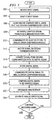
- FIGURE 5 is a flow chart 500 illustrating one example for a method of operation for circuit 100.
- Sampling switch 101 receives an input signal at step 502.
- Sampling switch 101 samples the input signal to generate a sampled signal at step 504.
- Sampling switch 101 then communicates the sampled signal down two parallel communication paths at step 506.
- sampling switch 108 On the first communication path, sampling switch 108 re-samples the sampled signal to generate a re-sampled signal at step 508, and the re-sampled signal is communicated to analog error comparison module 110 at step 510
- analog buffer 102 stores the sampled signal for a predetermined amount of time at step 512.
- Decision slicer 104 then converts the first sampled signal into a digital signal at step 514.
- Switch-and-latch 106 stores the digital signal for a period of time at step 516. Because the digital signal provided to switch-and-latch 106 is based on the sampled signal, switch-and-latch 106 does not need to respond to the digital signal at the input signal frequency, but rather at the sampling rate of sampling switch 101. After the digital signal has been stored for some amount of time, the digital signal is communicated to analog error comparison module at step 518.
- Analog error comparison module 110 compares the re-sampled signal to the digital signal at step 520. Based on the comparison, analog error comparison module 110 determines the amount of analog error in the input signal at step 522. From this analog error, analog error comparison module 110 generates an analog error signal at step 524. The analog error signal may be amplified to a suitable level in order to facilitate detection by other components. If the input signal continues to be received, then the method may be repeated from step 502. Otherwise, the method ends.
Landscapes
- Engineering & Computer Science (AREA)
- Theoretical Computer Science (AREA)
- Analogue/Digital Conversion (AREA)
- Electronic Switches (AREA)
- Dc Digital Transmission (AREA)
Applications Claiming Priority (4)
| Application Number | Priority Date | Filing Date | Title |
|---|---|---|---|
| US54614504P | 2004-02-20 | 2004-02-20 | |
| US546145P | 2004-02-20 | ||
| US821034 | 2004-04-08 | ||
| US10/821,034 US6977600B2 (en) | 2004-02-20 | 2004-04-08 | Determining analog error using parallel path sampling |
Publications (1)
| Publication Number | Publication Date |
|---|---|
| EP1566890A1 true EP1566890A1 (de) | 2005-08-24 |
Family
ID=34713857
Family Applications (1)
| Application Number | Title | Priority Date | Filing Date |
|---|---|---|---|
| EP05250673A Ceased EP1566890A1 (de) | 2004-02-20 | 2005-02-07 | Analogfehlerbestimmung unter Verwendung von Abtastung in parallelen Zweigen |
Country Status (5)
| Country | Link |
|---|---|
| US (1) | US6977600B2 (de) |
| EP (1) | EP1566890A1 (de) |
| JP (1) | JP4634182B2 (de) |
| KR (1) | KR100689004B1 (de) |
| CN (1) | CN100505547C (de) |
Families Citing this family (8)
| Publication number | Priority date | Publication date | Assignee | Title |
|---|---|---|---|---|
| JP4779793B2 (ja) * | 2006-05-01 | 2011-09-28 | 株式会社デンソー | Ad変換装置及び電子制御装置 |
| WO2013137911A1 (en) * | 2012-03-16 | 2013-09-19 | Song Sanquan | Apparatus and system for switching equalization |
| KR102074824B1 (ko) * | 2012-09-10 | 2020-02-07 | 한국전자통신연구원 | 신호 변환 전자 장치 및 신호 변환 전자 장치의 동작 방법 |
| JP6128802B2 (ja) * | 2012-11-07 | 2017-05-17 | キヤノン株式会社 | ファクシミリ装置及びその制御方法とプログラム |
| JP2014099705A (ja) * | 2012-11-13 | 2014-05-29 | Canon Inc | 通信装置及びその制御方法、並びにプログラム |
| US8958501B2 (en) * | 2012-11-26 | 2015-02-17 | Broadcom Corporation | Quasi-digital receiver for high speed SER-DES |
| WO2015136971A1 (ja) * | 2014-03-14 | 2015-09-17 | オムロン株式会社 | 制御システム |
| EP4145151B1 (de) * | 2022-07-18 | 2024-05-08 | Rohde & Schwarz GmbH & Co. KG | Signalverarbeitungsmodul und messinstrument |
Citations (5)
| Publication number | Priority date | Publication date | Assignee | Title |
|---|---|---|---|---|
| US5266952A (en) * | 1992-03-30 | 1993-11-30 | Hughes Aircraft Company | Feed forward predictive analog-to-digital converter |
| US6313780B1 (en) * | 1998-09-30 | 2001-11-06 | U.S. Philips Corporation | Analogue to digital converter |
| US20020175843A1 (en) * | 2001-05-23 | 2002-11-28 | Sameer Sonkusale | True background calibration of pipelined analog digital converters |
| US20030080894A1 (en) * | 2001-10-25 | 2003-05-01 | Takashi Konno | A/D converter |
| WO2004010586A2 (en) * | 2002-07-20 | 2004-01-29 | Koninklijke Philips Electronics N.V. | Switched-current analogue-to-digital converter |
Family Cites Families (9)
| Publication number | Priority date | Publication date | Assignee | Title |
|---|---|---|---|---|
| JPH07193507A (ja) * | 1993-12-27 | 1995-07-28 | Yokogawa Electric Corp | 直流信号測定用a/d変換器 |
| JPH10188590A (ja) * | 1996-12-25 | 1998-07-21 | Canon Inc | サンプルホールド回路 |
| JP2000031824A (ja) * | 1998-07-13 | 2000-01-28 | Nec Corp | A/dコンバータ用オフセットキャンセルコンパレータ |
| US6177899B1 (en) * | 1998-07-29 | 2001-01-23 | Etrend Electronics, Inc. | Analog-to-digital converter having multiple reference voltage comparators and boundary voltage error correction |
| US6160441A (en) * | 1998-10-30 | 2000-12-12 | Volterra Semiconductor Corporation | Sensors for measuring current passing through a load |
| DE10025566C2 (de) * | 2000-05-24 | 2003-04-30 | Infineon Technologies Ag | Verfahren und Vorrichtung zur Taktregelung eines digitalen Empfängers |
| JP2004010586A (ja) * | 2002-06-11 | 2004-01-15 | Teijin Chem Ltd | 環状ホスホネート化合物 |
| US6753801B2 (en) * | 2002-08-23 | 2004-06-22 | Micron Technology, Inc. | Fully differential reference driver for pipeline analog to digital converter |
| ITMI20030136A1 (it) * | 2003-01-28 | 2004-07-29 | St Microelectronics Srl | Stadio di ingresso a condensatori commutati per convertitori analogico-digitali. |
-
2004
- 2004-04-08 US US10/821,034 patent/US6977600B2/en not_active Expired - Lifetime
-
2005
- 2005-02-07 EP EP05250673A patent/EP1566890A1/de not_active Ceased
- 2005-02-17 JP JP2005040220A patent/JP4634182B2/ja not_active Expired - Fee Related
- 2005-02-18 CN CNB2005100093365A patent/CN100505547C/zh not_active Expired - Fee Related
- 2005-02-19 KR KR1020050013910A patent/KR100689004B1/ko not_active Expired - Fee Related
Patent Citations (5)
| Publication number | Priority date | Publication date | Assignee | Title |
|---|---|---|---|---|
| US5266952A (en) * | 1992-03-30 | 1993-11-30 | Hughes Aircraft Company | Feed forward predictive analog-to-digital converter |
| US6313780B1 (en) * | 1998-09-30 | 2001-11-06 | U.S. Philips Corporation | Analogue to digital converter |
| US20020175843A1 (en) * | 2001-05-23 | 2002-11-28 | Sameer Sonkusale | True background calibration of pipelined analog digital converters |
| US20030080894A1 (en) * | 2001-10-25 | 2003-05-01 | Takashi Konno | A/D converter |
| WO2004010586A2 (en) * | 2002-07-20 | 2004-01-29 | Koninklijke Philips Electronics N.V. | Switched-current analogue-to-digital converter |
Non-Patent Citations (1)
| Title |
|---|
| BRACEY M ET AL: "A 70 MS/s 8-bit differential switched-current CMOS A/D converter using parallel interleaved pipelines", MICROELECTRONICS AND VLSI, 1995. TENCON '95., IEEE REGION 10 INTERNATIONAL CONFERENCE ON HONG KONG 6-10 NOV. 1995, NEW YORK, NY, USA,IEEE, US, 6 November 1995 (1995-11-06), pages 143 - 146, XP010160068, ISBN: 0-7803-2624-5 * |
Also Published As
| Publication number | Publication date |
|---|---|
| CN1658509A (zh) | 2005-08-24 |
| KR20060042126A (ko) | 2006-05-12 |
| US6977600B2 (en) | 2005-12-20 |
| CN100505547C (zh) | 2009-06-24 |
| JP2005236995A (ja) | 2005-09-02 |
| US20050184898A1 (en) | 2005-08-25 |
| JP4634182B2 (ja) | 2011-02-16 |
| KR100689004B1 (ko) | 2007-03-08 |
Similar Documents
| Publication | Publication Date | Title |
|---|---|---|
| CN102112931B (zh) | 时间测量电路、时间测量方法、以及使用其的时间数字转换器和测试装置 | |
| US10673452B1 (en) | Analog-to-digital converter with interpolation | |
| US6967514B2 (en) | Method and apparatus for digital duty cycle adjustment | |
| US5920209A (en) | Time counting circuit, sampling circuit, skew adjusting circuit, and logic analyzing circuit | |
| KR102000544B1 (ko) | 아날로그 디지털 변환장치 및 방법 | |
| US7212580B2 (en) | Multi-level signal clock recovery technique | |
| KR20240090351A (ko) | 지연 기반 비교기 | |
| US10962933B1 (en) | Multibit per stage pipelined time-to-digital converter (TDC) | |
| KR20010072576A (ko) | 스큐에 민감하지 않은 저 전압 차동 수신기 | |
| US6977600B2 (en) | Determining analog error using parallel path sampling | |
| CN100414843C (zh) | 具有偏移补偿功能的突发模式接收装置及其数据恢复方法 | |
| US7298800B2 (en) | Analog signal control method, analog signal controller, and automatic gain controller | |
| EP1371137B1 (de) | Schnelle komparatoren mit verriegelungsstufe | |
| US10892769B2 (en) | Analog-to-digital converter with hysteresis | |
| CN113162586A (zh) | 一种时钟占空比修调方法及系统 | |
| JPH1093406A (ja) | タイミング発生装置 | |
| EP1321946A2 (de) | Schnelle, differenzielle Datenabtastschaltung | |
| US6940331B2 (en) | Delayed tap signal generating circuit for controlling delay by interpolating two input clocks | |
| JPH08340325A (ja) | 高速データ受信回路 | |
| JPH0846492A (ja) | 位相同期回路 | |
| JP5023605B2 (ja) | ディレイ調整回路およびその制御方法 | |
| US7944264B2 (en) | Variable delay circuit, variable delay circuit controlling method, and input/output circuit | |
| JP3077815B2 (ja) | パルス信号発生回路 | |
| KR0165822B1 (ko) | 오프셋 조절 장치 | |
| CN118350328A (zh) | 一种高线性度、高增益的时间误差放大器及其设计方法 |
Legal Events
| Date | Code | Title | Description |
|---|---|---|---|
| PUAI | Public reference made under article 153(3) epc to a published international application that has entered the european phase |
Free format text: ORIGINAL CODE: 0009012 |
|
| AK | Designated contracting states |
Kind code of ref document: A1 Designated state(s): AT BE BG CH CY CZ DE DK EE ES FI FR GB GR HU IE IS IT LI LT LU MC NL PL PT RO SE SI SK TR |
|
| AX | Request for extension of the european patent |
Extension state: AL BA HR LV MK YU |
|
| 17P | Request for examination filed |
Effective date: 20060220 |
|
| AKX | Designation fees paid |
Designated state(s): DE FR GB |
|
| STAA | Information on the status of an ep patent application or granted ep patent |
Free format text: STATUS: THE APPLICATION HAS BEEN REFUSED |
|
| 18R | Application refused |
Effective date: 20120725 |