EP1566852B1 - Piezoelektrisches Betätigungsglied, Uhr und elektronisches Gerät - Google Patents
Piezoelektrisches Betätigungsglied, Uhr und elektronisches Gerät Download PDFInfo
- Publication number
- EP1566852B1 EP1566852B1 EP05003440A EP05003440A EP1566852B1 EP 1566852 B1 EP1566852 B1 EP 1566852B1 EP 05003440 A EP05003440 A EP 05003440A EP 05003440 A EP05003440 A EP 05003440A EP 1566852 B1 EP1566852 B1 EP 1566852B1
- Authority
- EP
- European Patent Office
- Prior art keywords
- oscillator
- fastening part
- piezoelectric element
- piezoelectric actuator
- wiring substrate
- Prior art date
- Legal status (The legal status is an assumption and is not a legal conclusion. Google has not performed a legal analysis and makes no representation as to the accuracy of the status listed.)
- Expired - Lifetime
Links
- 239000000758 substrate Substances 0.000 claims description 100
- 238000009413 insulation Methods 0.000 claims description 22
- 229910052751 metal Inorganic materials 0.000 claims description 17
- 239000002184 metal Substances 0.000 claims description 17
- 230000010355 oscillation Effects 0.000 description 108
- 238000001514 detection method Methods 0.000 description 37
- RYGMFSIKBFXOCR-UHFFFAOYSA-N Copper Chemical compound [Cu] RYGMFSIKBFXOCR-UHFFFAOYSA-N 0.000 description 29
- 239000011889 copper foil Substances 0.000 description 29
- 238000005452 bending Methods 0.000 description 28
- 230000007246 mechanism Effects 0.000 description 23
- 230000000694 effects Effects 0.000 description 7
- 238000000034 method Methods 0.000 description 5
- 238000003466 welding Methods 0.000 description 5
- 239000004020 conductor Substances 0.000 description 4
- 230000007423 decrease Effects 0.000 description 4
- 238000005476 soldering Methods 0.000 description 4
- 230000008859 change Effects 0.000 description 3
- 230000008602 contraction Effects 0.000 description 3
- 238000006073 displacement reaction Methods 0.000 description 3
- 238000004519 manufacturing process Methods 0.000 description 3
- 230000010287 polarization Effects 0.000 description 3
- 238000003825 pressing Methods 0.000 description 3
- JQJCSZOEVBFDKO-UHFFFAOYSA-N lead zinc Chemical compound [Zn].[Pb] JQJCSZOEVBFDKO-UHFFFAOYSA-N 0.000 description 2
- 239000000463 material Substances 0.000 description 2
- 239000000203 mixture Substances 0.000 description 2
- NJPPVKZQTLUDBO-UHFFFAOYSA-N novaluron Chemical compound C1=C(Cl)C(OC(F)(F)C(OC(F)(F)F)F)=CC=C1NC(=O)NC(=O)C1=C(F)C=CC=C1F NJPPVKZQTLUDBO-UHFFFAOYSA-N 0.000 description 2
- 229910052706 scandium Inorganic materials 0.000 description 2
- SIXSYDAISGFNSX-UHFFFAOYSA-N scandium atom Chemical compound [Sc] SIXSYDAISGFNSX-UHFFFAOYSA-N 0.000 description 2
- 238000000926 separation method Methods 0.000 description 2
- 229910001220 stainless steel Inorganic materials 0.000 description 2
- 239000010935 stainless steel Substances 0.000 description 2
- 239000002033 PVDF binder Substances 0.000 description 1
- 229910003781 PbTiO3 Inorganic materials 0.000 description 1
- 239000004642 Polyimide Substances 0.000 description 1
- 230000009471 action Effects 0.000 description 1
- 239000000853 adhesive Substances 0.000 description 1
- 230000001070 adhesive effect Effects 0.000 description 1
- 229910002113 barium titanate Inorganic materials 0.000 description 1
- JRPBQTZRNDNNOP-UHFFFAOYSA-N barium titanate Chemical compound [Ba+2].[Ba+2].[O-][Ti]([O-])([O-])[O-] JRPBQTZRNDNNOP-UHFFFAOYSA-N 0.000 description 1
- 238000006243 chemical reaction Methods 0.000 description 1
- 230000001419 dependent effect Effects 0.000 description 1
- 230000006866 deterioration Effects 0.000 description 1
- NKZSPGSOXYXWQA-UHFFFAOYSA-N dioxido(oxo)titanium;lead(2+) Chemical compound [Pb+2].[O-][Ti]([O-])=O NKZSPGSOXYXWQA-UHFFFAOYSA-N 0.000 description 1
- 238000009826 distribution Methods 0.000 description 1
- 210000004709 eyebrow Anatomy 0.000 description 1
- 230000005484 gravity Effects 0.000 description 1
- 238000009434 installation Methods 0.000 description 1
- 230000002452 interceptive effect Effects 0.000 description 1
- 238000002955 isolation Methods 0.000 description 1
- QNZFKUWECYSYPS-UHFFFAOYSA-N lead zirconium Chemical compound [Zr].[Pb] QNZFKUWECYSYPS-UHFFFAOYSA-N 0.000 description 1
- GQYHUHYESMUTHG-UHFFFAOYSA-N lithium niobate Chemical compound [Li+].[O-][Nb](=O)=O GQYHUHYESMUTHG-UHFFFAOYSA-N 0.000 description 1
- 230000001050 lubricating effect Effects 0.000 description 1
- 238000005259 measurement Methods 0.000 description 1
- 229920000728 polyester Polymers 0.000 description 1
- 229920001721 polyimide Polymers 0.000 description 1
- 229920002981 polyvinylidene fluoride Polymers 0.000 description 1
- 230000008569 process Effects 0.000 description 1
- 239000010453 quartz Substances 0.000 description 1
- 230000004044 response Effects 0.000 description 1
- 230000000630 rising effect Effects 0.000 description 1
- 239000010979 ruby Substances 0.000 description 1
- 229910001750 ruby Inorganic materials 0.000 description 1
- 230000035939 shock Effects 0.000 description 1
- VYPSYNLAJGMNEJ-UHFFFAOYSA-N silicon dioxide Inorganic materials O=[Si]=O VYPSYNLAJGMNEJ-UHFFFAOYSA-N 0.000 description 1
- 238000004088 simulation Methods 0.000 description 1
- 125000006850 spacer group Chemical group 0.000 description 1
- -1 that is Substances 0.000 description 1
- 239000011701 zinc Substances 0.000 description 1
Images


Classifications
-
- G—PHYSICS
- G04—HOROLOGY
- G04C—ELECTROMECHANICAL CLOCKS OR WATCHES
- G04C13/00—Driving mechanisms for clocks by primary clocks
- G04C13/08—Secondary clocks actuated intermittently
- G04C13/12—Secondary clocks actuated intermittently by continuously-rotating electric motors
-
- H—ELECTRICITY
- H02—GENERATION; CONVERSION OR DISTRIBUTION OF ELECTRIC POWER
- H02N—ELECTRIC MACHINES NOT OTHERWISE PROVIDED FOR
- H02N2/00—Electric machines in general using piezoelectric effect, electrostriction or magnetostriction
- H02N2/0005—Electric machines in general using piezoelectric effect, electrostriction or magnetostriction producing non-specific motion; Details common to machines covered by H02N2/02 - H02N2/16
- H02N2/001—Driving devices, e.g. vibrators
- H02N2/003—Driving devices, e.g. vibrators using longitudinal or radial modes combined with bending modes
- H02N2/004—Rectangular vibrators
-
- H—ELECTRICITY
- H02—GENERATION; CONVERSION OR DISTRIBUTION OF ELECTRIC POWER
- H02N—ELECTRIC MACHINES NOT OTHERWISE PROVIDED FOR
- H02N2/00—Electric machines in general using piezoelectric effect, electrostriction or magnetostriction
- H02N2/0005—Electric machines in general using piezoelectric effect, electrostriction or magnetostriction producing non-specific motion; Details common to machines covered by H02N2/02 - H02N2/16
- H02N2/0075—Electrical details, e.g. drive or control circuits or methods
- H02N2/0085—Leads; Wiring arrangements
-
- H—ELECTRICITY
- H02—GENERATION; CONVERSION OR DISTRIBUTION OF ELECTRIC POWER
- H02N—ELECTRIC MACHINES NOT OTHERWISE PROVIDED FOR
- H02N2/00—Electric machines in general using piezoelectric effect, electrostriction or magnetostriction
- H02N2/10—Electric machines in general using piezoelectric effect, electrostriction or magnetostriction producing rotary motion, e.g. rotary motors
- H02N2/103—Electric machines in general using piezoelectric effect, electrostriction or magnetostriction producing rotary motion, e.g. rotary motors by pressing one or more vibrators against the rotor
Definitions
- the present invention relates to a piezoelectric actuator having a piezoelectric element, a timepiece having this piezoelectric actuator, and an electronic device.
- Piezoelectric elements feature excellent response and high conversion efficiency converting electrical energy to mechanical energy.
- various types of piezoelectric actuators using the piezoelectric effect of such piezoelectric elements have been developed in recent years and are used in such applications as piezoelectric buzzers, ultrasonic motors, and inkjet heads for printers.
- Piezoelectric actuators have also been proposed for use in applications with a strong need for miniaturization, such as driving the calendar display mechanism in wristwatches. (See, for example, Japanese Unexamined Patent Appl. Pub. 2001-286166.)
- the present invention is directed to the foregoing problem, and an object of this invention is to provide a piezoelectric actuator that makes wiring the piezoelectric elements simple, a timepiece having this piezoelectric actuator, and an electronic device.
- a piezoelectric actuator has an oscillator that has a flat base layer and a piezoelectric element layer on the base layer and oscillates as a result of a drive signal applied to the piezoelectric element, a driven member that is driven by vibration of the oscillator, a fastening part for securing the oscillator, and a wiring substrate secured to the fastening part for applying a drive signal for driving the piezoelectric element from a drive circuit to the piezoelectric element.
- the wiring substrate has a conductive member extending to an electrode disposed to the piezoelectric element.
- the conductive member is formed from a conductive elastic member that applies pressure to the electrode.
- the wiring substrate comprises a metal layer and an insulation layer or insulation sheet covering an entire surface of the metal layer; and the conductive member is a flat spring rendered in unison with the metal layer. This arrangement facilitates assembly because soldering or other bonding method is not required for wiring to the piezoelectric elements.
- the oscillator has a first piezoelectric element layer on the front side of the base layer and a second piezoelectric element layer on the back side of the base layer; wiring substrates are secured to both front and back sides of the fastening part; and the conductive member extending to the electrode disposed to the first piezoelectric element is disposed to the wiring substrate secured to the front of the fastening part, and the conductive member extending to the electrode disposed to the second piezoelectric element is disposed to the wiring substrate secured to the back of the fastening part.
- this desirable configuration also has a conductive part providing conductivity between the wiring substrates secured respectively to the front and back sides of the fastening part.
- Fig. 1 is a plan view showing the arrangement of a calendar display mechanism having a piezoelectric actuator A according to this embodiment of the invention disposed in a wristwatch.
- this piezoelectric actuator A has a base plate 102, a rectangular oscillator 10, and a rotor 100.
- the rotor 100 is the driven member that is driven by the oscillator 10. Vibration of the oscillator 10 against the outside surface of the rotor 100 causes the rotor 100 to rotate clockwise and transfer drive power to the date display wheel 50.
- This rotor 100 is connected to the ring-shaped date display wheel 50 through an intervening speed-reducing gear train containing the date-turning intermediate wheel 40 and date-turning wheel 60.
- This date display wheel 50 is what is driven by the rotor 100, and the date display wheel 50 is rotationally driven in conjunction with rotor 100 drive.
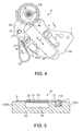
- Fig. 4 is a plan view of the piezoelectric actuator A
- Fig. 5 is a section view through section V-V shown in Fig. 4
- Fig. 6 and Fig. 7 are enlarged views of the rotor 100
- Fig. 8 is a section view showing the support structure of the rotor 100
- Fig. 9 is a section view describing how the pressure is adjusted using the pressure adjusting cam
- Fig. 10 is an exploded oblique view of the oscillator 10
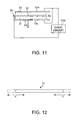
- Fig. 11 is a drive schematic showing supplying a drive signal to the piezoelectric element
- Fig. 12 to Fig. 14 describe the oscillation states of the oscillator
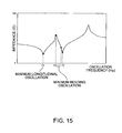
- Fig. 15 shows the relationship between impedance and the oscillation frequency of the oscillator 10.
- the oscillator 10 is fastened to the fastening part mounting portion 102A of the base plate 102 by screwing a screw 13 through the positioning hole 11A into the fastening part mounting portion 102A.
- a supporting contact portion 12 is also formed projecting from the piezoelectric elements 30, 31 on the opposite side as the fastening part 11 of the base layer 32, and this supporting contact portion 12 is placed on the supporting contact portion mounting portion 102B of the base plate 102 as shown in Fig. 5.
- the oscillator 10 is disposed with the fastening part 11 and supporting contact portion 12, which project to both sides from the part of the base layer 32 disposed between the piezoelectric elements 30, 31, placed on the base plate 102.
- the oscillator 10 is thus mounted to the base plate 102 by means of the fastening part 11 and supporting contact portion 12 with a space formed between the base plate 102 and the base layer 32 and piezoelectric elements 30, 31. While the supporting contact portion 12 rests on the base plate 102, the fastening part 11 is firmly fastened by a screw 13 to the base plate 102.
- a channel 100A that is arc-shaped in section is formed circumferentially to the outside surface of the rotor 100. Separation of the rotor 100 is also prevented by the contact part 36 contacting the bottom of this channel 100A. Furthermore, because the channel 100A is formed with an arc-shaped (curved) section and the contact part 36 that contacts this channel 100A is also arc-shaped, the channel 100A and contact part 36 touch at a point, thereby assuring the stable transfer of energy. Note, further, that this channel could alternatively be rectangularly shaped as indicated by the channel 100A' of rotor 100' shown in Fig. 7.
- the pressure adjusting cam 26 pushes against the distal end part of the spring part 23.
- this pressure adjusting cam 26 has a through-hole 26A.
- a screw-receiving part 26B planted in the base plate 102 is fit into this through-hole 26A, and the inside of the screw-receiving part 26B is threaded to receive a screw 27.
- a spacer 28 intervenes between the pressure adjusting cam 26 and base plate 102, and tightening the screw 27 fixes the pressure adjusting cam 26 to the base plate 102 while restricting rotary movement of the pressure adjusting cam 26.
- Loosening the screw 27 enables the pressure adjusting cam 26 to turn rotationally around the screw 27.
- the user can insert a substantially L-shaped adjustment terminal 29 in the terminal guide hole 26C rendered in the pressure adjusting cam 26, and by manually turning this adjustment terminal 29 can easily adjust the rotation of the pressure adjusting cam 26.
- the pressure applied to the oscillator 10 can be adjusted by adjusting the pressure adjusting cam 26. If the pressure adjusting cam 26 is turned to greatly deform the spring part 23 as indicated by the dotted line in Fig. 4, the rotor mounting part 25 is displaced clockwise as seen in the figure around the shaft 21 in resistance to the elastic force of the spring part 23, and the pressure applied by the rotor 100 to the oscillator 10 increases. If the pressure adjusting cam 26 is adjusted so that the gap between the two legs of the spring part 23 increases as indicated by the solid line in the figure, the elastic force of the spring part 23 decreases and the pressure applied by the rotor 100 to the oscillator 10 decreases. Note that the pressure adjusting cam 26 can be adjusted manually or the pressure adjusting cam 26 can be adjusted automatically by an automated assembly machine used for automatically assembling timepiece movements.
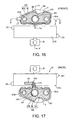
- Rectangular power supply electrodes 33A, 33B are bonded on the front and back sides of the piezoelectric element 30 on the top side of the base layer 32 so as to substantially cover the surface of the piezoelectric element 30.
- Rectangular power supply electrodes 33C, 33D are likewise bonded on the front and back sides of the piezoelectric element 31 on the bottom side of the base layer 32 so as to substantially cover the surface of the piezoelectric element 31.
- a rectangular detection electrode 34 (see Fig. 17) extending toward one end from substantially the lengthwise center of the oscillator 10 is also formed to power supply electrode 33C, and is electrically isolated from other areas of the detection electrode 33C by a cut. This detection electrode 34 is used to acquire a detection signal indicating oscillation of the oscillator 10.
- Materials that can be used for the piezoelectric elements 30, 31 include zirconium lead titanate (PZT (R)), quartz, lithium niobate, barium titanate, lead titanate, lead meta-niobate, polyvinylidene fluoride, lead zinc niobate, and lead scandium niobate.
- an AC drive signal is supplied from the drive circuit 500 to the power supply electrode 33A, base layer 32, and power supply electrode 33C so that the potential of the power supply electrode 33A, base layer 32, and power supply electrode 33C goes to +V, V DD , and +V (or -V, V DD , -V) where V DD is the ground potential of the drive circuit 500.
- the +V drive signal and the -V drive signal are AC signals of opposite phase.
- the power supply electrodes 33B and 33D contacting the piezoelectric elements 30, 31 can be omitted, and are therefore not shown in Fig. 11.
- the oscillator 10 thus produces oscillation combining longitudinal oscillation and bending oscillation, but whether the longitudinal oscillation mode is dominant or the bending oscillation mode is dominant depends on the frequency of the drive signal supplied to the piezoelectric elements 30, 31.
- Fig. 15 shows an example of the relationship between the oscillation frequency of the oscillator 10 and impedance. As shown in the figure, the resonance frequency f1 at which longitudinal oscillation mode impedance is lowest, and the resonance frequency f2 at which the bending oscillation impedance is lowest, are different.
- the piezoelectric elements 30, 31 vibrate in a longitudinal oscillation mode and bending oscillation is induced if the piezoelectric elements 30, 31 are driven at a frequency f2' between the resonance frequency f2 of the bending oscillation mode and the frequency f3 at which impedance is greatest between resonance frequency f1 and resonance frequency f2. Furthermore, driving the piezoelectric elements 30, 31 at a frequency f2' near the resonance frequency f2 of the bending oscillation mode produces a large bending oscillation, and the contact part 36 of the oscillator 10 traces a larger elliptical path.
- Drive efficiency is defined by the work done by the rotor 100 per unit time (that is, speed vs torque load) relative to the electrical energy supplied to the piezoelectric elements 30, 31.
- Fig. 16 is a plan view showing the top (front) of the oscillator 10
- Fig. 17 is a plan view showing the bottom (back) of the oscillator 10
- Fig. 18 is a section view through line A-A' in Fig. 16. Note that the power supply electrodes 33A and 33C and detection electrode 34 are not shown in the section view shown in Fig. 18.
- Two lead substrates 14A, 14B are used, one for drive signal input lines for supplying drive signals from the drive circuit 500 to the power supply electrodes 33A, 33C disposed to the piezoelectric elements 30, 31 to apply drive signals to the oscillator 10, and one for detection signal output lines for supplying detection signal output from the detection electrode 34 of the piezoelectric element 31 to the drive circuit 500 to output the oscillation state of the oscillator 10.
- these lead substrates 14A, 14B are disposed to the fastening part 11 of the oscillator 10.
- a height adjusting member 80 is fixed to the top and bottom sides of the fastening part 11 by adhesion or welding, and the lead substrates 14A, 14B are fixed by adhesion or welding to the height adjusting member 80.
- the height adjusting member 80 is used so that the elevation of the lead substrates 14A, 14B is above the piezoelectric elements 30, 31 referenced to the base layer 32 (fastening part 11).
- the lead substrates 14A, 14B have a conductive film of copper foil 15 disposed to an insulation layer 16 made of polyimide, for example. More specifically, substantially the entire top surface of the lead substrate 14A on the front side of the fastening part 11 is covered by a single copper foil 15A layer. Connecting part 17A extending toward the oscillator 10 is then disposed to this copper foil 15A. As shown in Fig. 18, this connecting part 17 is rendered as an overhang from the insulation layer 16 as shown in Fig. 18 and functions as the wire (conducting member) connecting the lead substrate 14A and power supply electrode 33A with the distal end of the connecting part 17 connected to the power supply electrode 33A. The connection between the connecting part 17A and power supply electrode 33A is made by soldering or low resistance welding to assure the reliability of the connection.
- connection part 17B functions as the line connecting the lead substrate 14B to the detection electrode 34
- connecting part 17C functions as the line connecting the lead substrate 14B to the power supply electrode 33C.
- the distal end of the connecting part 17B is thus connected to the power supply electrode 33C disposed to the surface of the piezoelectric element 31, and the distal end of the connecting part 17C is connected to the detection electrode 34.
- the connections between these connecting parts 17B, 17C and the detection electrode 34 and power supply electrode 33C are also made by soldering or low resistance welding to assure connection reliability.
- the connecting parts 17A, 17B, 17C formed as extensions of the copper foil layers 15A, 15B, 15C on lead substrates 14A, 14B are thus used as the wiring lines for connection to the power supply electrodes 33A, 33C and detection electrode 34 in this embodiment of the invention.
- This arrangement simplifies the task of making wiring connections, and thus affords more efficient assembly when compared with connecting the oscillator 10 to the lead substrates 14A, 14B by means of separate wiring leads or other discrete members.
- the load of the wiring on the oscillator 10 can also be reduced, oscillation of the oscillator 10 can be stabilized, and the effect on the movement of the piezoelectric actuator A can be suppressed as a result.
- connection to the piezoelectric element 30 on the front side of the base layer 32 is made from the lead substrate 14A on the top side of the fastening part 11, and the connection to the piezoelectric element 31 on the back of the base layer 32 is made from the lead substrate 14B on the bottom of the fastening part 11.
- the line from the lead substrate must be routed from the piezoelectric element on the front around to the piezoelectric element on the back of the base layer 32. Such routing is not necessary with the arrangement of the present invention, however, and the load of wiring on the oscillator 10 can therefore be reduced and vibration of the oscillator 10 can be stabilized.
- the power supply electrodes 33A, 33C and detection electrode 34 are disposed to locations corresponding to nodes in the vibration of the oscillator 10 in this embodiment of the invention, separation of the connecting parts 17A - 17C connected to the power supply electrodes 33A, 33C and detection electrode 34 due to vibration of the oscillator 10 can be prevented. Furthermore, because particularly high connection strength is not required between the connecting parts 17A - 17C and the power supply electrodes 33A, 33C and detection electrode 34, making the connections between the connecting parts 17A - 17C and power supply electrodes 33A, 33C and detection electrode 34 is easier, and assembly performance is improved.
- This embodiment of the invention further uses an intervening height adjusting member 80 to assemble the lead substrates 14A, 14B to the fastening part 11. Therefore, when connecting the connecting parts 17A, 17B, 17C extending from the lead substrates 14A, 14B to the power supply electrodes 33A, 33C and detection electrode 34, the connecting parts 17A, 17B, 17C do not bear on the piezoelectric elements 30, 31. Instead, the connecting part 17A extends directly to the power supply electrode 33A from above the piezoelectric element 30, and connecting parts 17B, 17C extend directly to the power supply electrode 33C and detection electrode 34 from below the piezoelectric element 31. As a result, the load applied by the connecting parts 17A, 17B, 17C on the oscillator 10 can be reduced.
- Drive signals of the same phase are supplied to the power supply electrode 33A and power supply electrode 33C in this embodiment of the invention. More specifically, the copper foil 15A connected to the power supply electrode 33A and the copper foil 15C connected to the power supply electrode 33C are electrically connected and drive signals of the same phase are supplied to the power supply electrodes 33A, 33C. This arrangement is further described below with reference to Fig. 19.
- Fig. 19 is a section view through line B-B' in Fig. 16.
- the circuit board 18 to which the drive circuit 500 is mounted is disposed to the base plate 102 with the side of the circuit board 18 on which the copper foil 18A conduction pattern is provided facing up as shown in this figure.
- the lead substrate 14B on the bottom of the fastening part 11 is pressed from above to the circuit board 18, thereby directly connecting the copper foil 18A of the circuit board 18 to the copper foil 15B, 15C of the lead substrate 14B, and thus electrically connecting the circuit board 18 and lead substrate 14B.
- a conduction spring 37 extending from the lead substrate 14A toward the circuit board 18 is disposed to the copper foil 15A of the lead substrate 14A on the top side of the fastening part 11.
- the distal end 37A of this conduction spring 37 extends to a position below where the circuit board 18 is disposed.
- the conduction spring 37 is deflected upwards and the distal end 37A presses against the copper foil 18A on the top of the circuit board 18.
- the copper foil 18A on the circuit board 18 and the copper foil 15A on the lead substrate 14A are thus electrically connected. Because the circuit board 18 and lead substrate 14B are thus electrically connected, conduction is also established between the lead substrate 14A and lead substrate 14B.
- the ground potential V DD of the drive circuit 500 is applied to the base layer 32.
- This V DD voltage is applied to the base layer 32 by applying V DD to the fastening part 11 of the base layer 32 in this embodiment of the invention.
- the lead substrate 14A disposed on the top side of the fastening part 11 does not completely cover the surface of the fastening part 11 when seen from above, but instead leaves a part of the fastening part 11 exposed.
- a ground conductor 81 providing a connection to the ground potential (voltage V DD ) of the drive circuit 500 (the foregoing circuit board 18) is connected to this exposed part 11B.
- the copper foil 15A connected to the power supply electrode 33A and the copper foil 15C connected to the power supply electrode 33C are electrically connected, drive signals of the same phase can be supplied to the power supply electrodes 33A, 33C, and voltage V DD can be applied to the base layer 32.
- the oscillator 10 and lead substrates 14A, 14B are assembled as a unit, and conductivity to the circuit board 18 is made when this unit assembled into the piezoelectric actuator A. This arrangement is described below.
- two guide pins 150A, 150B project from the base plate 102 in addition to the fastening part mounting portion (threaded pin) 102A.
- two pin holes 151A, 151B through which the guide pins 150A, 150B pass are formed in the fastening part 11 in addition to the positioning hole 11A to which the fastening part mounting portion 102A is inserted.
- Fig. 19 shows that two guide pins 150A, 150B project from the base plate 102 in addition to the fastening part mounting portion (threaded pin) 102A.
- two pin holes 151A, 151B through which the guide pins 150A, 150B pass are formed in the fastening part 11 in addition to the positioning hole 11A to which the fastening part mounting portion 102A is inserted.
- positioning hole 140 and pin holes 152A, 152B to which the base plate 102 and guide pins 150A, 150B are inserted are also formed in the lead substrates 14A, 14B, and positioning hole 153 and pin holes 153A, 153B to which the fastening part mounting portion 102A and guide pins 150A, 150B are inserted are likewise formed in the height adjusting member 80.
- the fastening part 11, lead substrates 14A, 14B, and height adjusting member 80 are thus layered in the order lead substrate 14B, height adjusting member 80, fastening part 11, height adjusting member 80, and lead substrate 14A, and are fixed by adhesion or welding, for example.
- the various members are positioned so that the respectively formed positioning holes and pin holes overlap.
- the connecting part 17A extending from the copper foil 15A of the lead substrate 14A is also bonded to the power supply electrode 33A
- the connecting part 17B extending from the copper foil 15B on lead substrate 14B is bonded to the detection electrode 34
- the connecting part 17C extending from the copper foil 15C on the lead substrate 14B is bonded to the power supply electrode 33C
- the lead substrates 14A, 14B are thus assembled in unity with the fastening part 11, and the oscillator 10 and lead substrates 14A, 14B thus form a single unit.
- the oscillator 10 thus integrated with the lead substrates 14A, 14B is assembled to the base plate 102 by fitting the fastening part 11 to the fastening part mounting portion 102A and guide pins 150A, 150B disposed to the base plate 102.
- the distal end 37A of the conduction spring 37 disposed to the lead substrate 14A also presses against the copper foil 18A of the circuit board 18 disposed to the base plate 102, thereby establishing conductivity between the lead substrate 14A and circuit board 18.
- the copper foil 15B, 15C on the lead substrate 14B touches the copper foil 18A of the circuit board 18, thereby providing conductivity between the lead substrate 14B and circuit board 18.
- the lead substrates 14A, 14B are positioned relative to the circuit board 18 by means of part mounting portion 102A and guide pins 150A, 150B, and do not need to be individually positioned.
- the top of the lead substrate 14A is covered by insulation layer 154 and thus electrically isolated from the other parts of the wristwatch, and a pressure plate 155 is then disposed over the insulation layer 154.
- a pressure plate 155 is then disposed over the insulation layer 154.
- the oscillator 10 and lead substrates 14A, 14B form an integrated unit in this embodiment of the invention, assembly, including mounting the oscillator 10 to the base plate 102 and connecting the oscillator 10 to the circuit board 18, is easier and quality can be stabilized. Furthermore, because common parts, that is, the fastening part mounting portion 102A and guide pins 150A, 150B, are used for positioning the fastening part 11 and lead substrates 14A, 14B, the fastening part 11 and lead substrates 14A, 14B do not need to be positioned individually.
- the lead substrates 14A, 14B are connected to the piezoelectric elements 30, 31 using extensions of the copper foil layers 15A, 15B, 15C on the lead substrates 14A, 14B in this embodiment of the invention.
- the invention shall not be so limited, however.
- an arrangement in which a flat spring is connected individually to each of the lead substrates 14A, 14B and used to wire the lead substrates 14A, 14B to the piezoelectric elements 30, 31 could alternatively be used. This arrangement is further described with reference to Fig. 21 to Fig. 23.
- Fig. 21 is a plan view showing the top (front) of an oscillator 10 not being an embodiment of the invention as claimed
- Fig. 22 is a plan view showing the bottom (back) of this oscillator 10
- Fig. 23 is a section view through line C-C' in Fig. 21. Note that the power supply electrodes 33A to 33D and detection electrode 34 are not shown in the section view in Fig. 23.
- lead substrate 14A in this embodiment of the invention comprises an insulation layer 85 and a metal layer 15A' bonded to the top of the insulation layer 85
- the lead substrate 14B comprises an insulation layer 85 and two physically separated metal layers 15B', 15C' bonded to the top of the insulation layer 85.
- This insulation layer 85 replaces the foregoing insulation layer 16, and metal layers 15A' to 15C' replace the foregoing copper foil layers 15A - 15C.
- a flat spring 17A' is connected to metal layer 15A' as a wiring member for connection to the power supply electrode 33A
- a flat spring 17B' is connected to metal layer 15B' as a wiring member for connection to the detection electrode 34
- flat spring 17C' is connected to metal layer 15C' as a wiring member for connection to the power supply electrode 33C.
- the flat springs 17A' - 17C' can be welded or otherwise connected to the metal layers 15A' - 15C', or these members can be integrally formed.
- flat spring 17A' is bent in an inverted V shape with the distal end contacting the power supply electrode 33A at a point from above the piezoelectric element 30, thereby reducing the load applied to the piezoelectric element 30 by contact with the flat spring 17A'.
- the distal ends of the other flat springs 17B', 17C' likewise contact the power supply electrode 33C and detection electrode 34 at a point from below the piezoelectric element 31, thereby reducing the load applied to the piezoelectric element 31 by contact with the flat springs 17B', 17C'.
- the wiring is thus prevented from interfering with oscillation of the oscillator 10.
- the metal layers 15A' - 15C' could be bonded to the fastening part 11 using a non-conductive adhesive instead of interposing an insulation layer 85 between the fastening part 11 and the metal layers 15A' - 15C'.
- This arrangement reduces the number of parts needed for isolation, thus reducing cost and affording a thinner, smaller configuration.
- the lead substrates 14A, 14B could be manufactured using a single flexible printed circuit 14'.
- This flexible printed circuit 14' has a copper foil 15' conduction pattern bonded to a dielectric sheet 16' of polyester, for example.
- the dielectric sheet 16' is bonded to the height adjusting member 80 on the front or back side of the fastening part 11 so that the copper foil 15' is to the outside, then bent around the fastening part 11 and bonded to the opposite end of the height adjusting member 80 on the back or front side of the fastening part 11.
- the cost can be reduced and conductivity between the front and back sides of the fastening part 11 is easily provided.
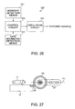
- the drive circuit 500 has a midnight detection means 501, control circuit 503, date advancing detection means 502, and oscillation circuit 504.
- the midnight detection means 501 is a mechanical switch assembled in the movement 73 (see Fig. 2) and outputs a control signal to the control circuit 503 when the time turns to 12:00 midnight.
- the main parts of the date advancing detection means 502 are the foregoing spring 64 and contact 65 (see Fig. 1), and the date advancing detection means 502 outputs a control signal to the control circuit 503 when the spring 64 and contact 65 make contact, that is, when completion of advancing the date is detected.
- the control circuit 503 outputs an oscillation control signal to the oscillation circuit 504 based on the control signal supplied from the midnight detection means 501 and the control signal supplied from the date advancing detection means 502.
- This oscillation control signal goes from LOW to HIGH when midnight is detected by the midnight detection means 501, and drops from HIGH to LOW when the date advancing detection means 502 detects that the data has been advanced.
- the oscillation circuit 504 is powered when this oscillation control signal goes HIGH, and power supply to the oscillation circuit 504 stops when the oscillation control signal goes LOW.
- the oscillation control signal is HIGH, a drive signal of a specified frequency is supplied through the power supply electrodes 33A to 33D to the piezoelectric elements 30, 31.
- this drive signal is thus applied, the piezoelectric elements 30, 31 expand and contract as described above.
- the date-turning intermediate wheel 40 turns one revolution when the date changes, but this occurs only at a specific time at midnight. It is therefore sufficient for the oscillation circuit 504 to oscillate only during this time.
- operation of the oscillation circuit 504 is stopped completely when it is not necessary to drive the date-turning intermediate wheel 40. Unnecessary power consumption by the oscillation circuit 504 can thus be reduced.
- the midnight detection means 501 shown in Fig. 26 detects that midnight has come, and the oscillation control signal is output from the control circuit 503 to the oscillation circuit 504.
- a drive signal of a specific frequency is supplied from the oscillation circuit 504 through the power supply electrodes 33A to 33D to the piezoelectric elements 30, 31.
- the drive signal is supplied from the drive circuit 500 to the power supply electrodes 33A to 33D, the piezoelectric elements 30, 31 vibrate due to expansion and contraction, and the oscillator 10 thus oscillates longitudinally.
- the drive circuit 500 supplies AC drive signals so that the potential of the top, middle, and bottom are respectively +V, V DD , +V (or -V, V DD , -V).
- the oscillator 10 When the oscillator 10 is thus electrically excited longitudinally, an imbalance in the weight balance of the oscillator 10 mechanically induces a bending oscillation.
- the contact part 36 oscillates along an elliptical path and drives the rotor 100.
- the drive circuit 500 stops supplying the drive signal when the spring 64 and contact 65 shown in Fig. 1 make contact. When the spring 64 and contact 65 touch, the distal end 64a has dropped into the notch 4c. The date-turning intermediate wheel 40 then starts turning.
- the small diameter portion 4a rotates while sliding in contact with the teeth 6a, 6b of the date-turning wheel 60.
- the notch 4c then reaches the position of a tooth 6a of the date-turning wheel 60, that tooth 6a engages the notch 4c.
- the date-turning wheel 60 moves in conjunction with the date-turning intermediate wheel 40 and turns clockwise one tooth, that is, 1/5 revolution.
- the date display wheel 50 also turns clockwise the distance of one tooth (that is, the distance equal to one day). Note that in short months having less than 31 days, the foregoing operation repeats multiple times so that the date display wheel 50 displays the correct date according to the calendar.
- the date-turning intermediate wheel 40 then continues advancing counterclockwise until the notch 4c reaches the position of the distal end 64a of the spring 64, at which point the spring 64 enters the notch 4c.
- the spring 64 and contact 65 thus make contact, drive signal supply ends, and the date-turning intermediate wheel 40 stops turning.
- the date-turning intermediate wheel 40 thus turns one revolution per day.
- the operator When assembling the timepiece movement, the operator sets the movement containing the piezoelectric actuator A on a rotational speed sensor not shown to detect the speed of the rotor 100.
- This rotational speed sensor is preferably a laser displacement sensor or other sensor for detecting the rotational speed without contacting the piece being tested.
- the operator then performs a specific operation to set the drive circuit 500 to an adjustment mode.
- This causes the control circuit 503 to output the oscillation control signal to the oscillation circuit 504, and the oscillation circuit 504 supplies drive signals of a specific frequency through the power supply electrodes 33A to 33D to the piezoelectric elements 30, 31.
- This causes the oscillator 10 to oscillate and begin driving the rotor 100 in conjunction with displacement of the contact part 36.
- the pressure can thus be adjusted manually by a procedure such as described above, or automatically using an automated assembly machine for automatically assembling timepiece movements.
- the operator can thus manually adjust the amount of applied pressure as described above, but the direction in which this pressure is applied is also important from the perspective of improving the drive efficiency of the rotor 100.
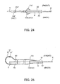
- Fig. 27 is a plan view showing the relative positions of the rotor 100 and oscillator 10 when the direction of the pressure applied by the rotor 100 to the oscillator 10 is 0°.
- Imaginary line P1 shown in the figure indicates the direction in which the rotor 100 can move. This line P1 is substantially parallel to the direction of oscillator 10 oscillation. Applying force to the rotor 100 in the direction of arrow a1 applies pressure to the contact part 36 in the direction of arrow b1.
- Fig. 28 and Fig. 29 are plan views showing the relative positions of the rotor 100 and oscillator 10 when the direction of the pressure applied by the rotor 100 to the oscillator 10 is 90°.
- Imaginary line P2 shown Fig. 28 indicates the direction in which the rotor 100 can move. This line P2 is substantially perpendicular to the oscillation direction of the oscillator 10. Applying force to the rotor 100 in the direction of arrow a2 applies pressure to the contact part 36 in the direction of arrow b2 (the direction perpendicular to the oscillation direction).
- Imaginary line P3 shown in Fig. 29 extends in the direction of oscillator 10 oscillation from the point of contact between the rotor 100 and contact part 36.
- the rotor 100 exerts pressure at substantially 90° to the contact part 36. That is, by applying force to the rotor 100 in the direction of arrow a3, pressure is applied in the direction of arrow b3 (perpendicular to the oscillation direction) to the contact part 36.
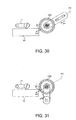
- Fig. 30 and Fig. 31 are plan views showing the relative positions of the rotor 100 and oscillator 10 when the direction of the pressure applied by the rotor 100 to the oscillator 10 is 30°.
- Imaginary line P4 shown Fig. 30 extends at a 30° angle to the oscillation direction of the oscillator 10 from the point of contact between the rotor 100 and contact part 36. Applying force to the rotor 100 in the direction of arrow a4 applies pressure to the contact part 36 in the direction of arrow b4 (that is, 30° to the oscillation direction).
- Imaginary line P5 shown in Fig. 31 extends at an angle of 30° to the oscillation direction of the oscillator 10 from the point of contact between the rotor 100 and contact part 36.
- the center of circular movement of the rotor 100 is located on a line perpendicular to this line P5 through the position at which line P5 is tangent.
- the rotor 100 applies pressure at a substantially 30° angle to the contact part 36.
- applying force to the rotor 100 in the direction of arrow a5 applies pressure to the contact part 36 in the direction of arrow b5 (inclined 30° to the oscillation direction).
- the longitudinal oscillation and secondary bending oscillation produced by the oscillator must be stabilized so that the contact part on the distal end of the oscillator moves periodically always tracing the same path.
- the oscillator used in a piezoelectric actuator is not a simple rectangular plate as described in the foregoing book, and has a contact part on the end. As a result, stable longitudinal oscillation and secondary bending oscillation cannot be achieved even if the ratio between long and short sides is as described.
- the piezoelectric elements measure 7 mm on the long side and 1.98 mm on the short side, and are made of PZT.
- the base layer is 0.1 mm thick stainless steel (SUS301).
- the contact part is 0.5 mm wide, projects 0.45 mm, and has a mass of 0.16 mg.
- the extension to the fastening part is 0.4 mm wide and 0.5 mm long.
- Fig. 33 The results of oscillation simulations using oscillators thus comprised with contact parts and without contact parts are shown in Fig. 33. Note that the values shown in parentheses () in Fig. 33 are the actual measurements. Based on the results shown in Fig. 33, we know that the presence of the contact part has a greater effect on secondary bending oscillation than on longitudinal oscillation, and providing this contact part increases the difference between the resonance frequency of the longitudinal oscillation and the resonance frequency of the secondary bending oscillation.
- changing the length b of the short side reduces the difference between the resonance frequency of the longitudinal oscillation and secondary bending oscillation modes, and can cancel the effect of the contact parts.
- the optimum ratio of the sides b/a of an oscillator is in the range b/a ⁇ 0.274 (1 > b/a).
- a thin piezoelectric actuator A suitable for installation in limited space such as inside a timepiece
- pressure is applied between the rotor 100 and oscillator 10 by pushing the rotor 100, which is the driven member, against the contact part 36 of the oscillator 10, and this pressure can be adjusted by rotating a pressure adjusting cam 26.
- this embodiment of the invention can fasten the oscillator 10 to the base plate 102 with no play (looseness). As a result, deterioration in the drive characteristics of the rotor 100 driven by vibration from the oscillator 10, and a drop in the durability of the oscillator 10, can be greatly improved.
- the connecting parts 17A, 17B, 17C formed as extensions of the copper foil layers 15A, 15B, 15C on the lead substrates 14A, 14B are also used for wiring to the power supply electrodes 33A, 33C and detection electrode 34 in this embodiment of the invention. Wiring is therefore easier than in an arrangement in which lead wires or other discrete members are used to connect the oscillator 10 and lead substrates 14A, 14B, and manufacturability is thus improved.
- the piezoelectric actuator A can also be efficiently driven by applying appropriate pressure to the oscillator 10.
- a lever 20 with a spring part 23 is used as the pressure mechanism for applying pressure to the oscillator 10 through the intervening rotor 100, and a pressure adjusting cam 26 is used as the adjustment mechanism for adjusting the applied pressure.
- the invention shall not be so limited, however, and can be varied as described below.
- the spring part could be shaped to fit inside this space (such as using a flat spring or coil spring).
- the spring part could also be disposed separately to the lever 20.
- the adjusting mechanism is also not limited to the pressure adjusting cam 26, and any structure capable of adjusting the elastic force generated by the spring part can be used.
- the number of intermediate gears intervening between the rotor 100 and date display wheel 50 is not limited to that shown in the foregoing embodiments, and a desirable number of gears can be used. Because the direction of rotor 100 rotation is determined by the number of intermediate gears, the relative positions of the rotor 100 and oscillator 10 must be adjusted accordingly.
- a oscillator 10 having two piezoelectric elements 30, 31 is described by way of example in the foregoing embodiment, but the present invention shall not be so limited and can be configured using an oscillator with only one piezoelectric element or a layered structure having three or more piezoelectric elements in the oscillator.
- a rectangular oscillator 10 is used in the foregoing embodiments, but the shape of the oscillator 10 shall not be limited to a rectangle and could be any shape with a long direction, including a trapezoid, parallelogram, rhombus, or triangle.
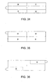
- the shape of the electrodes bonded to the piezoelectric elements shall also not be limited to the shape shown in Fig. 10, and could be formed to the piezoelectric elements as shown in Fig. 34 to Fig. 36.
- the oscillator is driven by supplying a drive signal to electrode I and electrode II.
- Longitudinal oscillation is produced from the electrode I part, oscillation is produced from the electrode II parts, and the electrode III parts do not vibrate.
- An imbalance relative to the longitudinal expansion and contraction is thus produced, a secondary bending oscillation is thereby excited, and the contact part is thus driven to oscillate along an elliptical path in a certain direction (such as clockwise).
- drive signals are supplied to electrode I and electrode III.
- longitudinal oscillation is produced from the electrode I part, oscillation is produced from the electrode III parts, and the electrode II parts do not vibrate.
- Fig. 35 shows a variation identical to that in Fig. 34 except that electrode I is eliminated.
- This oscillator can be driven in a longitudinal oscillation mode by supplying the drive signal to electrode II.
- Fig. 36 shows an arrangement driven by a single electrode I covering the entire surface of the oscillator. A secondary bending oscillation is excited in this oscillator due to the unbalanced shape (contact parts). As indicated by the dotted lines, electrodes III creating a part of the piezoelectric element that does not vibrate can also be provided.
- the oscillator 10 has a cantilevered structure in the piezoelectric actuator A described above.
- the present invention shall not be so limited, and screwing the supporting contact portion 12 to the supporting contact portion mounting portion 102B similarly to the fastening part 11 affords a piezoelectric actuator in which the oscillator 10 is secured at both ends.
- the foregoing piezoelectric actuator A also has the oscillator 10 and rotor 100 disposed to the base plate 102, but the invention shall not be limited to this base plate 102 and can use any structure that can support the parts of the piezoelectric actuator A.
- the foregoing embodiments are described by way of example using the piezoelectric actuator A as the piezoelectric actuator of a calendar display mechanism assembled into a timepiece.
- the present invention shall not be so limited, however, and can be used in a time display mechanism for displaying the time by means of hour, minute, and second hands.
- the invention can also be used for the piezoelectric actuator of such electronic devices as small fans, toys, and other entertainment devices.
- the foregoing piezoelectric actuator A is also well suited as a piezoelectric actuator used in battery-powered portable devices because the piezoelectric actuator can be rendered thin and small while providing high drive efficiency.
- the piezoelectric actuator A in the foregoing embodiments causes the contact part 36 of the oscillator 10 to oscillate along an elliptical path in order to produce drive power for driving a rotor 100 with extremely low electrical energy such as in a wristwatch.
- the present invention shall not be so limited, however, and the rotor 100 could be rotationally driven by causing the contact part 36 to operate in a longitudinal oscillation mode aligned with the lengthwise direction of the oscillator 10.
Landscapes
- Physics & Mathematics (AREA)
- General Physics & Mathematics (AREA)
- General Electrical Machinery Utilizing Piezoelectricity, Electrostriction Or Magnetostriction (AREA)
- Electromechanical Clocks (AREA)
Claims (11)
- Piezoelektrischer Aktor (A) mit einem Schwinger (10), der eine ebene Basisschicht (102) und eine piezoelektrische Elementschicht auf der Basisschicht (32) besitzt und als Ergebnis dessen schwingt, dass ein Antriebssignal an das piezoelektrische Element (30, 31) angelegt wird, und einem angetriebenen Element (100), das durch eine Vibration des Schwingers (10) angetrieben wird, wobei der piezoelektrische Aktor (A) aufweist:einem Befestigungsteil (11) zum Anbringen des Schwingers (10); undeinem Verdrahtungssubstrat (14A), das an dem Befestigungsteil (11) zum Anlegen eines Antriebssignals zum Antreiben des piezoelektrischen Elements (30, 31) von einer Antriebsschaltung (500) zu dem piezoelektrischen Element (30, 31) angebracht ist;wobei das Verdrahtungssubstrat (14A) ein leitfähiges Element (17) besitzt, das sich zu einer Elektrode (33A) erstreckt, die an dem piezoelektrischen Element (30, 31) vorgesehen ist; und gekennzeichnet durch:ein Höheneinstellelement (80), das zwischen dem Verdrahtungssubstrat (14A, 14B) und einem Befestigungsteil (11) derart wirkt, dass das leitfähige Element (17), das sich an dem Verdrahtungssubstrat erstreckt, höher ist als das piezoelektrische Element (30, 31).
- Piezoelektrischer Aktor (A) nach Anspruch 1, bei welchem:das Verdrahtungssubstrat (14A) eine Isolierschicht (16) und einen leitfähigen Film (15), der auf der Isolierschicht (16) vorgesehen ist, aufweist; unddas leitfähige Element (17) ist als eine Erweiterung des leitfähigen Films (15) gebildet.
- Piezoelektrischer Aktor (A) nach Anspruch 1, bei welchem das leitfähige Element (17A') aus einem leitfähigen elastischen Element gebildet, das einen Druck auf die Elektrode (33A) aufbringt.
- Piezoelektrischer Aktor (A) nach Anspruch 1, bei welchem:das Verdrahtungssubstrat (14A) eine Metallschicht (15A') und eine Isolierschicht (85) oder Isolierbahn, welche die gesamte Oberfläche der Metallschicht (15A') bedeckt, aufweist; unddas leitfähige Element ist eine ebene Feder (17A'), die integral mit der Metalllage (15A') gebildet ist.
- Piezoelektrischer Aktor (A) nach einem der Ansprüche 1 bis 4, bei welchem:der Schwinger (10) eine erste piezoelektrische Elementschicht (30) auf der Vorderseite der Basisschicht (32) und eine zweite piezoelektrische Elementschicht (31) auf der Rückseite der Basisschicht (32) besitzt;ein Verdrahtungssubstrat (14A, 14B), das sowohl an der Vorderseite als auch an der Rückseite des Befestigungsteils (11) angebracht ist; unddas leitfähige Element (17A), das sich zu der an dem ersten piezoelektrischen Element (30) vorgesehenen Elektrode (33A) erstreckt, ist an dem Verdrahtungssubstrat (14A) vorgesehen, das auf der Vorderseite des Befestigungsteils (11) angebracht ist, und das leitfähige Element (17C), das sich zu der an dem zweiten piezoelektrischen Element (31) vorgesehenen Elektrode (33C) erstreckt, ist an dem Verdrahtungssubstrat (14B) vorgesehen, das auf der Rückseite des Befestigungsteils (11) angebracht ist.
- Piezoelektrischer Aktor nach Anspruch 5, ferner umfassend ein leitfähiges Teil (37), das eine Leitfähigkeit zwischen den Verdrahtungssubtraten (14A, 14B) bereitstellt, die jeweils an der Vorderseite bzw. Rückseite des Befestigungsteils (11) angebracht sind.
- Piezoelektrischer Aktor (A) nach einem der Ansprüche 1 bis 3, bei welchem:der Schwinger (10) eine erste piezoelektrische Elementschicht (30) auf der Vorderseite der Basisschicht und eine zweite piezoelektrische Elementschicht (31) auf der Rückseite der Basisschicht (32) aufweist;das Verdrahtungssubstrat ist flexibel; unddas leitfähige Element (15') besitzt ein Ende, das an der Vorderseite des Befestigungsteils (11) angebracht ist, und ein anderes Ende, das an der Rückseite des Befestigungsteils (11) angebracht ist, wobei sich das leitfähige Element (15') zu dem ersten piezoelektrischen Element (30) erstreckt, das an dem einen Ende des Verdrahtungssubstrats (14') vorgesehen ist, das an der Vorderseite des Befestigungsteils (11) angebracht ist, und sich das leitfähige Element (15'), zu dem zweiten piezoelektrischen Element (31) erstreckt, das an dem anderen Ende des Verdrahtungssubstrats (14') vorgesehen ist, das an der Rückseite des Befestigungsteils (11) angebracht ist.
- Piezoelektrischer Aktor nach einem der Ansprüche 1 bis 7, bei welchem das Verdrahtungssubstrat (14A, 14B, 14') an dem Befestigungsteil befestigt ist, wodurch eine einzelne Einheit gebildet wird.
- Piezoelektrischer Aktor nach Anspruch 8, bei welchem das Befestigungsteil (11) und das Verdrahtungssubstrat (14A) durch ein Positionierelement (11A) positioniert sind.
- Uhr, umfassend:einen piezoelektrischen Aktor (A) nach einem der Ansprüche 1 bis 9;eine Antriebsschaltung (500) zum Ausgeben eines Antriebssignals zum Antreiben des Schwingers (10);eine Stromquelle zum Zuführen von Strom zu der Antriebsschaltung; undeine Zeitinformationseinrichtung, die durch den piezoelektrischen Aktor zum Anzeigen einer Zeitinformation einschließlich einer Kalenderinformation angetrieben ist.
- Elektronisches Gerät, umfassend:einen piezoelektrischen Aktor (A) nach einem der Ansprüche 1 bis 9;eine Antriebsschaltung (500) zum Ausgeben eines Antriebssignals zum Antreiben des Schwingers;eine Stromquelle zum Zuführen von Strom zu der Antriebsschaltung; undein angetriebenes Element (100), das durch den piezoelektrischen Aktor angetrieben ist.
Applications Claiming Priority (2)
| Application Number | Priority Date | Filing Date | Title |
|---|---|---|---|
| JP2004042396A JP2005237102A (ja) | 2004-02-19 | 2004-02-19 | 圧電アクチュエータ、時計及び電子機器 |
| JP2004042396 | 2004-02-19 |
Publications (3)
| Publication Number | Publication Date |
|---|---|
| EP1566852A2 EP1566852A2 (de) | 2005-08-24 |
| EP1566852A3 EP1566852A3 (de) | 2005-09-07 |
| EP1566852B1 true EP1566852B1 (de) | 2007-04-11 |
Family
ID=34709108
Family Applications (1)
| Application Number | Title | Priority Date | Filing Date |
|---|---|---|---|
| EP05003440A Expired - Lifetime EP1566852B1 (de) | 2004-02-19 | 2005-02-17 | Piezoelektrisches Betätigungsglied, Uhr und elektronisches Gerät |
Country Status (5)
| Country | Link |
|---|---|
| US (1) | US7109638B2 (de) |
| EP (1) | EP1566852B1 (de) |
| JP (1) | JP2005237102A (de) |
| CN (1) | CN100498593C (de) |
| DE (1) | DE602005000833T2 (de) |
Families Citing this family (26)
| Publication number | Priority date | Publication date | Assignee | Title |
|---|---|---|---|---|
| TWI300285B (en) * | 2005-03-18 | 2008-08-21 | Foxconn Tech Co Ltd | Piezoelectric motor |
| JP4857886B2 (ja) * | 2005-06-24 | 2012-01-18 | セイコーエプソン株式会社 | 圧電アクチュエータの耐衝撃装置、これを備えた電子機器 |
| US8884474B2 (en) * | 2006-06-02 | 2014-11-11 | MicroZeus, LLC | Method of fabricating a micro machine |
| US8159107B2 (en) * | 2006-06-02 | 2012-04-17 | Microzeus Llc | Micro rotary machine and methods for using same |
| US8134276B2 (en) * | 2006-06-02 | 2012-03-13 | MicroZeus, LLC | Methods and systems for positioning micro elements |
| WO2007143623A2 (en) | 2006-06-02 | 2007-12-13 | Stalford Harold L | Methods and systems for micro machines |
| US9156674B2 (en) * | 2006-06-02 | 2015-10-13 | MicroZeus, LLC | Micro transport machine and methods for using same |
| US8915158B2 (en) * | 2006-06-02 | 2014-12-23 | MicroZeus, LLC | Methods and systems for micro transmissions |
| US8282284B2 (en) * | 2006-06-02 | 2012-10-09 | MicroZeus, LLC | Methods and systems for micro bearings |
| JP2008136318A (ja) | 2006-11-29 | 2008-06-12 | Olympus Corp | 超音波モータ及び顕微鏡ステージ |
| JP5457651B2 (ja) * | 2008-02-18 | 2014-04-02 | 太平洋セメント株式会社 | 超音波モータ |
| US8122973B2 (en) | 2008-05-21 | 2012-02-28 | Stalford Harold L | Three dimensional (3D) robotic micro electro mechanical systems (MEMS) arm and system |
| CN102342012A (zh) * | 2009-03-02 | 2012-02-01 | 株式会社腾龙 | 振动电机单元、振动电机及使用振动电机的透镜驱动装置 |
| KR101188007B1 (ko) | 2010-06-21 | 2012-10-05 | 삼성전기주식회사 | 햅틱 피드백 액츄에이터, 햅틱 피드백 디바이스 및 전자장치 |
| JP5601996B2 (ja) * | 2010-12-06 | 2014-10-08 | 株式会社タムロン | 振動モータ及びレンズ駆動機構 |
| JP2012165496A (ja) * | 2011-02-03 | 2012-08-30 | Tamron Co Ltd | 振動モータ及びレンズ駆動機構 |
| JP2012210053A (ja) * | 2011-03-29 | 2012-10-25 | Seiko Epson Corp | 圧電アクチュエーター、ロボット及びロボットハンド |
| JP5776269B2 (ja) * | 2011-03-29 | 2015-09-09 | セイコーエプソン株式会社 | 圧電アクチュエーター、ロボット及びロボットハンド |
| US9136778B2 (en) * | 2012-02-29 | 2015-09-15 | Discovery Technology International, Inc. | Non-magnetic high-speed piezoelectric rotary motor |
| JP6025446B2 (ja) * | 2012-08-10 | 2016-11-16 | キヤノン株式会社 | 振動型アクチュエータ、撮像装置および、振動型アクチュエータを備えた装置 |
| JP6398454B2 (ja) * | 2014-08-13 | 2018-10-03 | セイコーエプソン株式会社 | 圧電駆動装置、ロボット、及び、それらの駆動方法 |
| JP6107894B2 (ja) * | 2015-07-02 | 2017-04-05 | セイコーエプソン株式会社 | 圧電アクチュエーター、ロボット及びロボットハンド |
| US20170092838A1 (en) * | 2015-09-29 | 2017-03-30 | Seiko Epson Corporation | Piezoelectric driving apparatus, method of manufacturing the same, motor, robot, and pump |
| JP6641944B2 (ja) * | 2015-12-03 | 2020-02-05 | セイコーエプソン株式会社 | モーター用圧電駆動装置およびその製造方法、モーター、ロボット、ならびにポンプ |
| US10833608B2 (en) * | 2016-08-03 | 2020-11-10 | Canon Kabushiki Kaisha | Vibration actuator and electronic apparatus using vibration actuator |
| EA035603B1 (ru) * | 2017-12-14 | 2020-07-15 | Ерлан Жандарбекович Джунусбеков | Устройство и виброгенератор для подавления акустических шумов |
Family Cites Families (3)
| Publication number | Priority date | Publication date | Assignee | Title |
|---|---|---|---|---|
| EP2568595A3 (de) | 1998-12-21 | 2013-05-15 | Seiko Epson Corporation | Piezoelektrischer Aktor, Uhrwerk und tragbares Gerät |
| JP4631124B2 (ja) | 2000-03-30 | 2011-02-16 | セイコーエプソン株式会社 | 圧電アクチュエータ、時計および機器 |
| DE60324247D1 (de) * | 2002-03-01 | 2008-12-04 | Seiko Epson Corp | Piezoelektrisches betätigungsglied und uhr und tragbare einheit mit piezoelektrischem betätigungsglied |
-
2004
- 2004-02-19 JP JP2004042396A patent/JP2005237102A/ja active Pending
-
2005
- 2005-02-17 DE DE602005000833T patent/DE602005000833T2/de not_active Expired - Lifetime
- 2005-02-17 EP EP05003440A patent/EP1566852B1/de not_active Expired - Lifetime
- 2005-02-17 CN CNB2005100084050A patent/CN100498593C/zh not_active Expired - Fee Related
- 2005-02-17 US US11/060,521 patent/US7109638B2/en not_active Expired - Lifetime
Also Published As
| Publication number | Publication date |
|---|---|
| CN100498593C (zh) | 2009-06-10 |
| CN1658093A (zh) | 2005-08-24 |
| US7109638B2 (en) | 2006-09-19 |
| EP1566852A3 (de) | 2005-09-07 |
| US20050184621A1 (en) | 2005-08-25 |
| DE602005000833T2 (de) | 2008-01-10 |
| EP1566852A2 (de) | 2005-08-24 |
| JP2005237102A (ja) | 2005-09-02 |
| DE602005000833D1 (de) | 2007-05-24 |
Similar Documents
| Publication | Publication Date | Title |
|---|---|---|
| EP1566852B1 (de) | Piezoelektrisches Betätigungsglied, Uhr und elektronisches Gerät | |
| US6909222B2 (en) | Piezoelectric actuator, and timepiece and portable equipment having the same | |
| CN101189787B (zh) | 压电致动器和具有该压电致动器的电子设备 | |
| CN101022254B (zh) | 压电振动体及其固有振动数调整方法、压电激励器及设备 | |
| US6885615B1 (en) | Piezoelectric actuator, time piece, and portable device | |
| JP4891053B2 (ja) | 超音波モータ | |
| US11233465B2 (en) | Piezoelectric drive device, robot, and printer | |
| JP4923548B2 (ja) | 圧電アクチュエータの駆動制御方法、圧電アクチュエータの駆動制御装置、および電子機器 | |
| JP2002223577A (ja) | 圧電アクチュエータ、時計、携帯機器、圧電アクチュエータの設計方法および製造方法 | |
| JP2000188882A (ja) | 駆動装置、カレンダー表示装置、携帯機器および時計 | |
| JP5974355B2 (ja) | 圧電アクチュエーター及び電子機器 | |
| JPH06121560A (ja) | 超音波モータ | |
| JP2011160525A (ja) | 圧電振動体装置、及び電子機器 | |
| JP4213737B2 (ja) | 圧電ステータのノーダルポイントを自動で探して支持する構造 | |
| US20040233793A1 (en) | Analog electronic timepiece | |
| JP2000188886A (ja) | 圧電アクチュエータおよび時計 | |
| JP2006136060A (ja) | 圧電アクチュエータおよび電子機器 | |
| JP4857572B2 (ja) | アクチュエータ、アクチュエータユニット、時計及び電子機器 | |
| JP3059043B2 (ja) | 超音波振動子、超音波モータ及び超音波モータを備えた装置 | |
| JPH07115783A (ja) | 棒状超音波振動子および棒状超音波モータ | |
| JP2007037242A (ja) | 圧電アクチュエータ、および電子機器 | |
| JP2003339177A (ja) | 超音波モータ及び超音波モータつき電子機器 | |
| JP2006050818A (ja) | 圧電アクチュエータ |
Legal Events
| Date | Code | Title | Description |
|---|---|---|---|
| PUAI | Public reference made under article 153(3) epc to a published international application that has entered the european phase |
Free format text: ORIGINAL CODE: 0009012 |
|
| PUAL | Search report despatched |
Free format text: ORIGINAL CODE: 0009013 |
|
| 17P | Request for examination filed |
Effective date: 20050217 |
|
| AK | Designated contracting states |
Kind code of ref document: A2 Designated state(s): AT BE BG CH CY CZ DE DK EE ES FI FR GB GR HU IE IS IT LI LT LU MC NL PL PT RO SE SI SK TR |
|
| AX | Request for extension of the european patent |
Extension state: AL BA HR LV MK YU |
|
| AK | Designated contracting states |
Kind code of ref document: A3 Designated state(s): AT BE BG CH CY CZ DE DK EE ES FI FR GB GR HU IE IS IT LI LT LU MC NL PL PT RO SE SI SK TR |
|
| AX | Request for extension of the european patent |
Extension state: AL BA HR LV MK YU |
|
| RIC1 | Information provided on ipc code assigned before grant |
Ipc: 7G 04C 13/12 B Ipc: 7H 01L 41/09 A |
|
| AKX | Designation fees paid |
Designated state(s): CH DE FR GB LI |
|
| GRAP | Despatch of communication of intention to grant a patent |
Free format text: ORIGINAL CODE: EPIDOSNIGR1 |
|
| GRAS | Grant fee paid |
Free format text: ORIGINAL CODE: EPIDOSNIGR3 |
|
| GRAA | (expected) grant |
Free format text: ORIGINAL CODE: 0009210 |
|
| AK | Designated contracting states |
Kind code of ref document: B1 Designated state(s): CH DE FR GB LI |
|
| REG | Reference to a national code |
Ref country code: GB Ref legal event code: FG4D |
|
| REG | Reference to a national code |
Ref country code: CH Ref legal event code: EP |
|
| REF | Corresponds to: |
Ref document number: 602005000833 Country of ref document: DE Date of ref document: 20070524 Kind code of ref document: P |
|
| REG | Reference to a national code |
Ref country code: CH Ref legal event code: NV Representative=s name: NOVAGRAAF INTERNATIONAL SA |
|
| ET | Fr: translation filed | ||
| PLBE | No opposition filed within time limit |
Free format text: ORIGINAL CODE: 0009261 |
|
| STAA | Information on the status of an ep patent application or granted ep patent |
Free format text: STATUS: NO OPPOSITION FILED WITHIN TIME LIMIT |
|
| 26N | No opposition filed |
Effective date: 20080114 |
|
| REG | Reference to a national code |
Ref country code: CH Ref legal event code: PFA Owner name: SEIKO EPSON CORPORATION Free format text: SEIKO EPSON CORPORATION#4-1, NISHI-SHINJUKU 2-CHOME#SHINJUKU-KU TOKYO 163-0811 (JP) -TRANSFER TO- SEIKO EPSON CORPORATION#4-1, NISHI-SHINJUKU 2-CHOME#SHINJUKU-KU TOKYO 163-0811 (JP) |
|
| REG | Reference to a national code |
Ref country code: FR Ref legal event code: PLFP Year of fee payment: 12 |
|
| REG | Reference to a national code |
Ref country code: FR Ref legal event code: PLFP Year of fee payment: 13 |
|
| PGFP | Annual fee paid to national office [announced via postgrant information from national office to epo] |
Ref country code: DE Payment date: 20170214 Year of fee payment: 13 Ref country code: CH Payment date: 20170214 Year of fee payment: 13 Ref country code: FR Payment date: 20170112 Year of fee payment: 13 |
|
| PGFP | Annual fee paid to national office [announced via postgrant information from national office to epo] |
Ref country code: GB Payment date: 20170215 Year of fee payment: 13 |
|
| REG | Reference to a national code |
Ref country code: DE Ref legal event code: R119 Ref document number: 602005000833 Country of ref document: DE |
|
| REG | Reference to a national code |
Ref country code: CH Ref legal event code: PL |
|
| GBPC | Gb: european patent ceased through non-payment of renewal fee |
Effective date: 20180217 |
|
| PG25 | Lapsed in a contracting state [announced via postgrant information from national office to epo] |
Ref country code: CH Free format text: LAPSE BECAUSE OF NON-PAYMENT OF DUE FEES Effective date: 20180228 Ref country code: LI Free format text: LAPSE BECAUSE OF NON-PAYMENT OF DUE FEES Effective date: 20180228 |
|
| REG | Reference to a national code |
Ref country code: FR Ref legal event code: ST Effective date: 20181031 |
|
| PG25 | Lapsed in a contracting state [announced via postgrant information from national office to epo] |
Ref country code: DE Free format text: LAPSE BECAUSE OF NON-PAYMENT OF DUE FEES Effective date: 20180901 |
|
| PG25 | Lapsed in a contracting state [announced via postgrant information from national office to epo] |
Ref country code: FR Free format text: LAPSE BECAUSE OF NON-PAYMENT OF DUE FEES Effective date: 20180228 Ref country code: GB Free format text: LAPSE BECAUSE OF NON-PAYMENT OF DUE FEES Effective date: 20180217 |